Week 06
Electronics Design
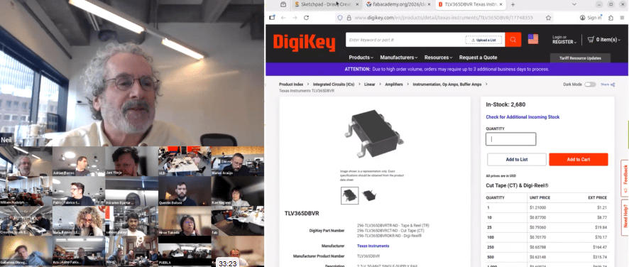
Class with Neil
During the theory class of Week 06, we focused on the fundamentals of Electronics Design. In this session, we learned about the basic principles involved in designing electronic circuits and how to create custom electronic boards. We explored essential electronic components such as resistors, capacitors, microcontrollers, and connectors, as well as how these elements interact within a circuit.
Additionally, we were introduced to the use of electronic design software to develop schematics and convert them into PCB layouts ready for fabrication. Concepts such as component placement, routing, and electrical connections were discussed to ensure proper functionality of the circuit.
This week helped me understand the process of transforming an electronic idea into a manufacturable circuit board. It is an important step toward integrating electronics into my final project, allowing me to design and produce custom boards tailored to the specific needs of my system.
Group Assignment:
°Use the test equipment in your lab to observe the operation of a microcontroller circuit board (as a minimum, you should demonstrate the use of a logic analyzer)
° Document your work on the group work page and reflect what you learned on your individual page
Have you answered these questions?
- I. Linked to the group assignment page. ✅
- II. Documented what you have learned in electronics design✅
- III.Checked your board can be fabricated ✅
- IV. Explained problems and how you fixed them. ✅
- V. Included original design files (Eagle, KiCad, etc.) ✅
- VI.Included a ‘hero shot’✅
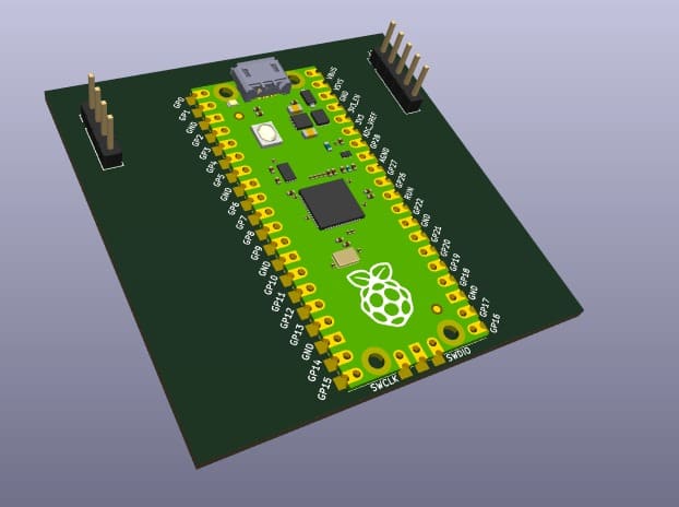
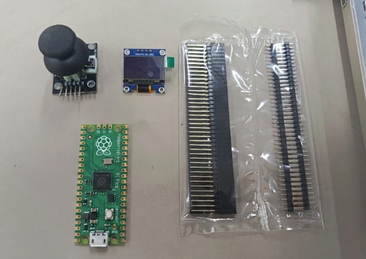
Hero Shot
This hero shot represents the final result of my Electronics Design assignment, where I designed a custom development board in KiCad integrating a Raspberry Pi Pico, a joystick module, and an OLED display. The project demonstrates the integration of electronic design, embedded systems, and user interaction in a single PCB, combining both input and output components into a functional prototype.
Through this assignment, I explored the complete PCB design workflow, including schematic creation, component organization, routing, and preparation for digital fabrication. The final board reflects the transition from a digital electronic design into a manufacturable hardware system capable of communication, visualization, and interactive control.
Group Assignment Sumary
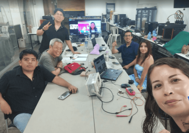
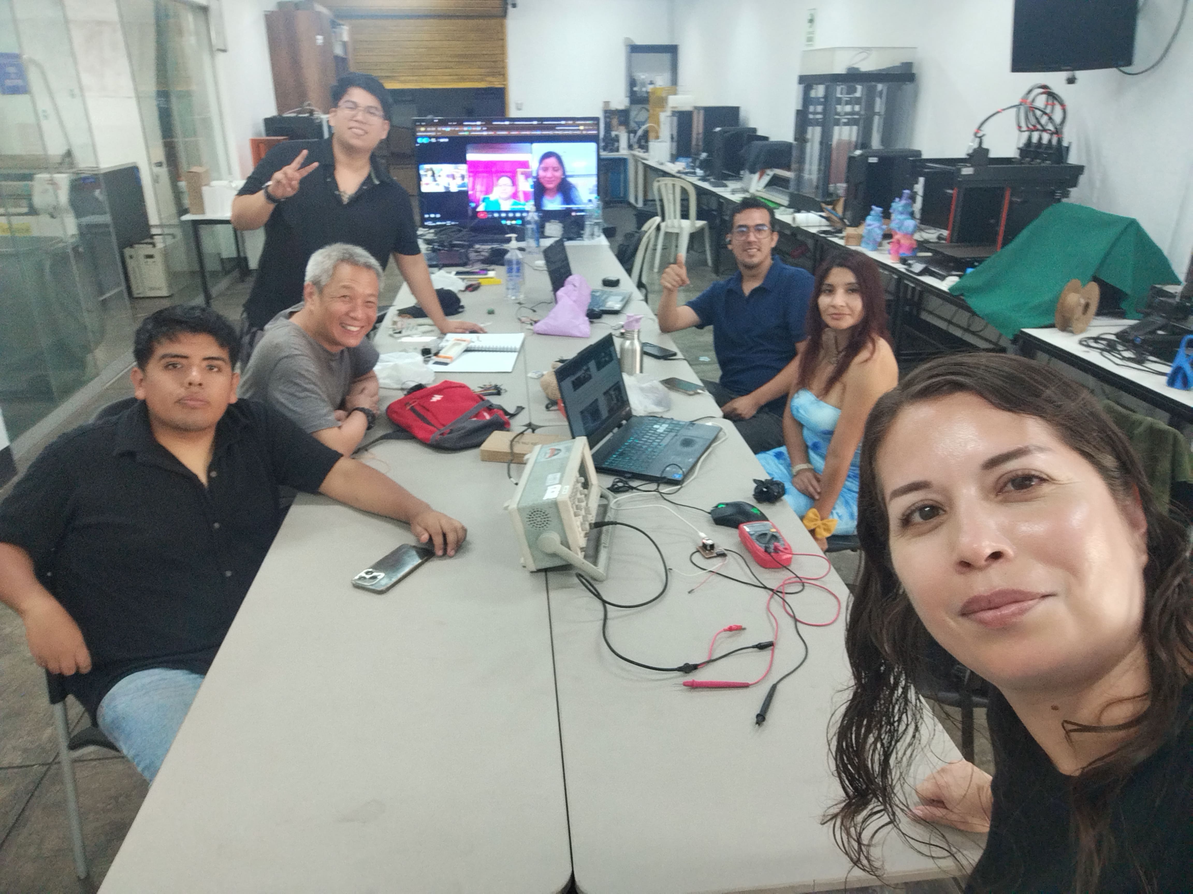
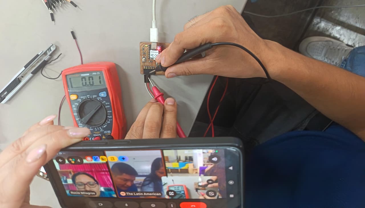
Before starting my individual work, we organized a Zoom meeting to coordinate the group assignment related to Electronics Design. During the meeting, we discussed the objective of analyzing the electrical behavior of a microcontroller board using measurement tools available in our labs. Each member shared the equipment they had access to, such as multimeters and oscilloscopes, and the type of boards they would test. This discussion allowed us to compare methods for measuring voltage stability and verifying digital signals, helping us better understand how microcontroller boards behave electrically and how to properly analyze their performance.
Here is the link to learn more about the group project.
Electronic Tools Used
During the Electronics Design week, we worked with different measurement and programming tools to evaluate and confirm the performance of our electronic board. These tools allowed us to generate and analyze electronic signals to verify that the circuit was functioning properly. Throughout the process, we observed signal waveforms, checked voltage levels, ensured there were no short circuits, and confirmed that the generated signal remained stable.
Tools Used for Signal Measurement
| 🔧 Tool | 📦 Model | 🛠️ How We Used It |
|---|---|---|
| 📊 Digital Oscilloscope | GW Instek GDS-1152A (150 MHz, 2-channel digital storage oscilloscope) | Visualized waveforms over time (square wave), verified voltage levels, and checked frequency stability. |
| 🔌 Digital Multimeter | PR-75 | Checked power rails (VCC/GND), confirmed the 3.3V logic level, and ruled out short circuits (continuity test). |
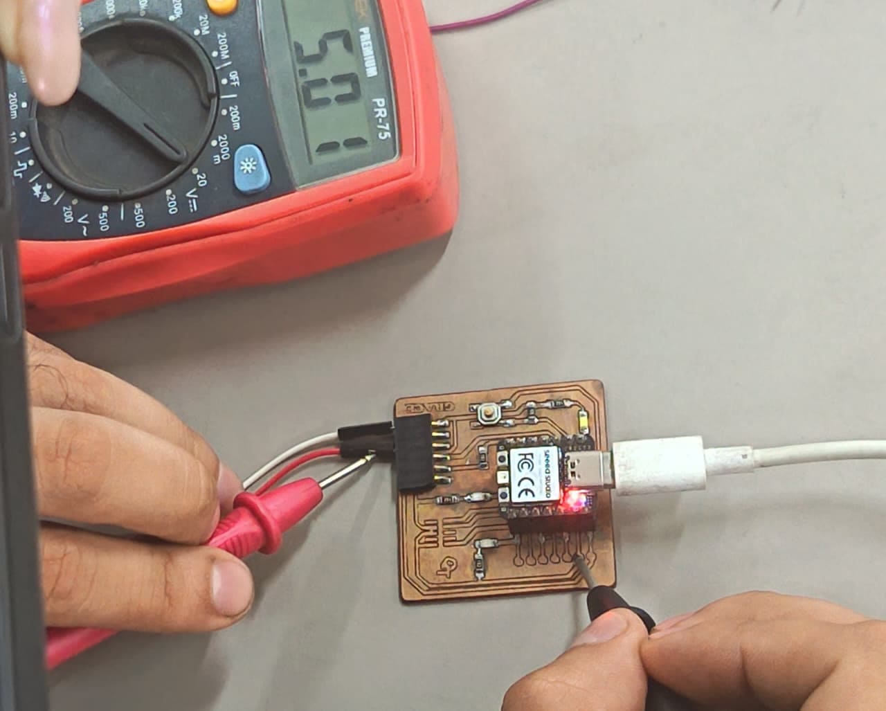
| 💻 Microcontroller Board | Custom PCB with Seeed Studio XIAO RP2040 | Generated a digital GPIO signal to be measured with the oscilloscope. |
| ⚡ Power Supply | USB | Powered and programmed the board. |
Procedure
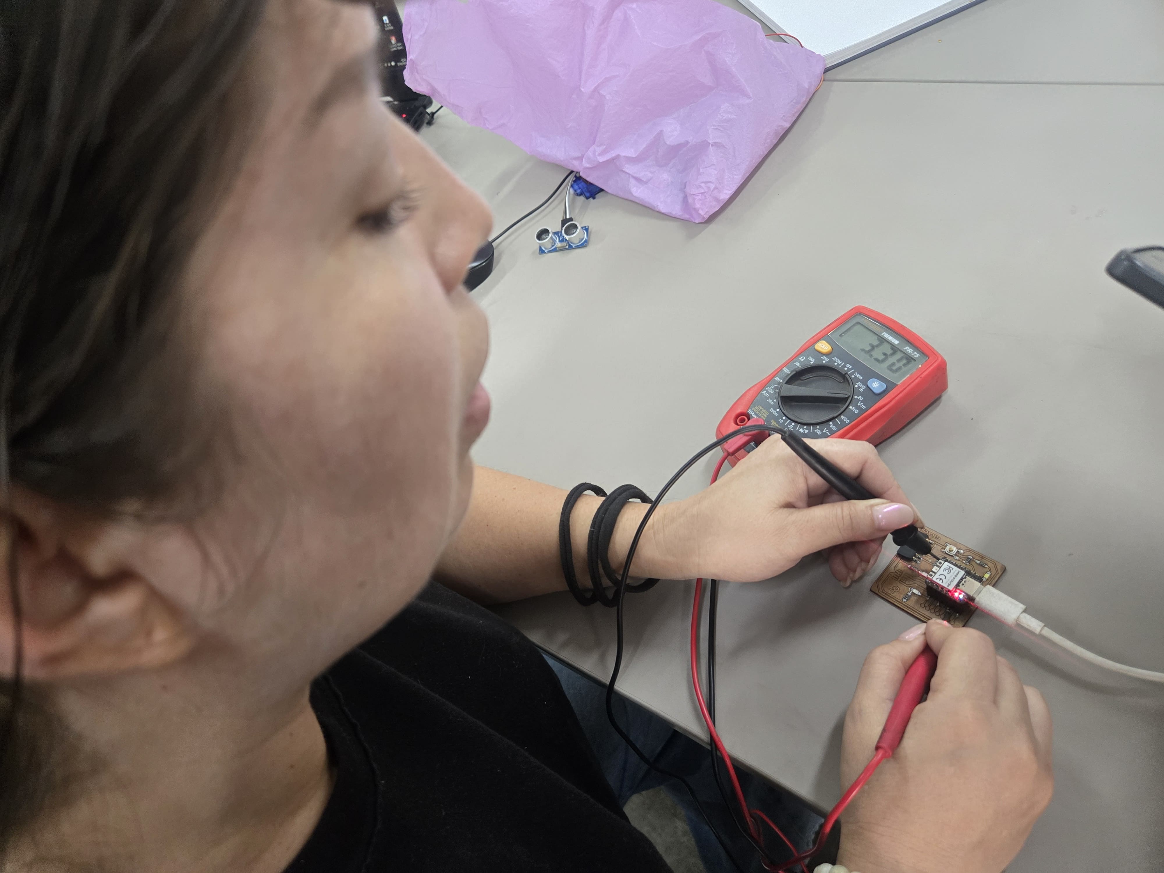
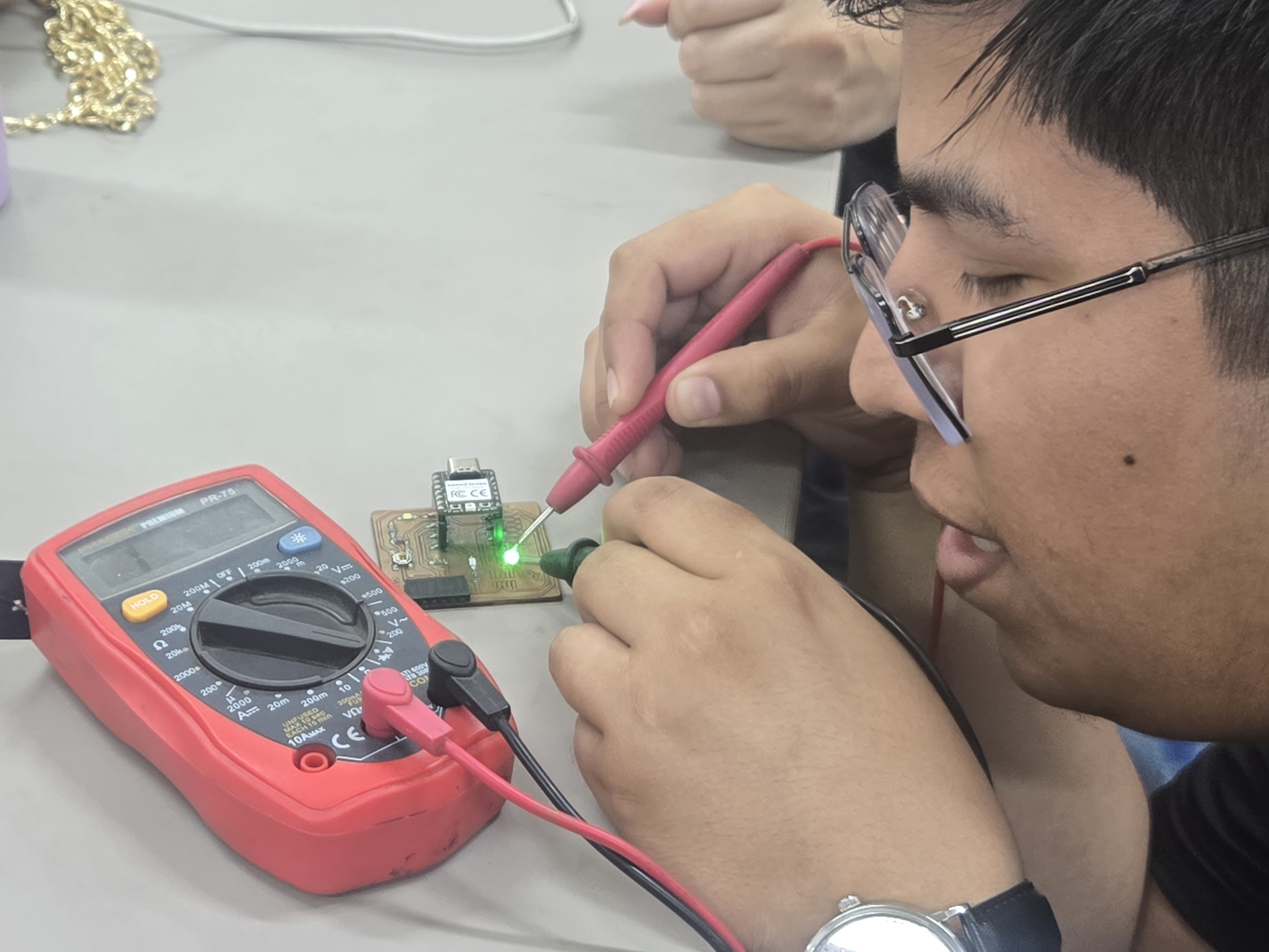
🔍 1. Multimeter Pre-Check
Before connecting the oscilloscope, we first used a digital multimeter to verify that the board was operating correctly and safely. This preliminary inspection helped us ensure that the electronic system was powered properly before measuring any signals.
- Confirmed that the board was receiving the correct power supply.
- Measured the voltage between GND and VCC.
- Verified that the 3.3V logic level was stable.
- Performed a continuity test to ensure there were no short circuits.
2. Oscilloscope Setup
After verifying that the board was operating correctly, we proceeded to connect the oscilloscope to observe the signal generated by the microcontroller.
Connection setup:
- ⚫ Ground clip (black) → Connected to the board GND
- 🔴 Probe tip → Connected to the GPIO output pin
Oscilloscope configuration:
- Channel: CH1
- Voltage scale: 1 V/div
- Time scale: 1 ms/div
- Trigger: Edge mode (CH1)
- Auto Setup used for initial calibration
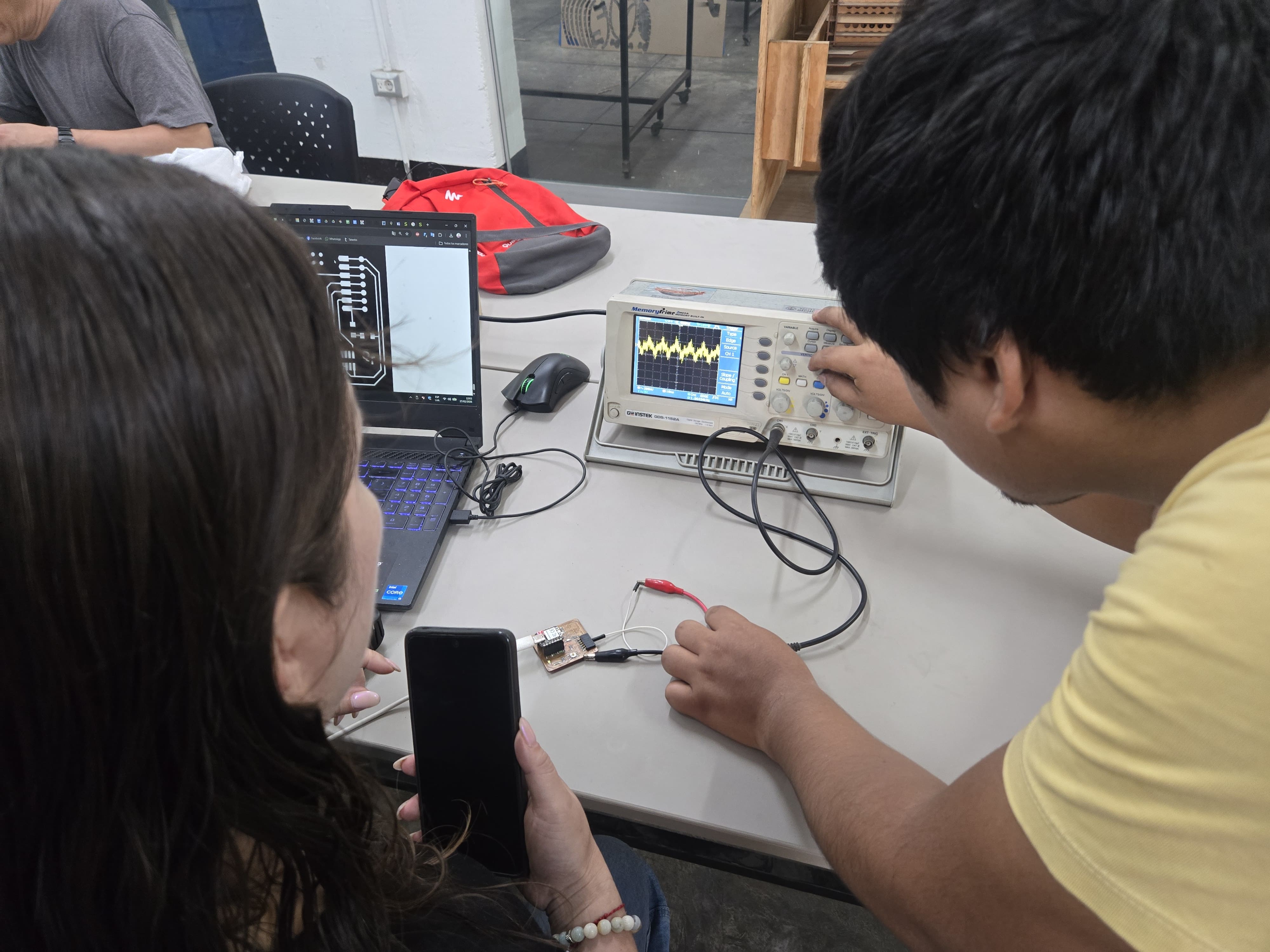
📊 3. Signal Observation
After programming the RP2040 to generate a square wave signal, we used the oscilloscope to analyze the behavior of the output signal on the GPIO pin.
- A clearly defined digital square wave was visible on the screen.
- Voltage levels varied between 0V and approximately 3.3V, matching the logic level of the board.
- The signal frequency remained stable and consistent with the programmed timing.
These observations confirmed that the microcontroller was executing the program correctly and that the GPIO pin was switching properly between digital states.
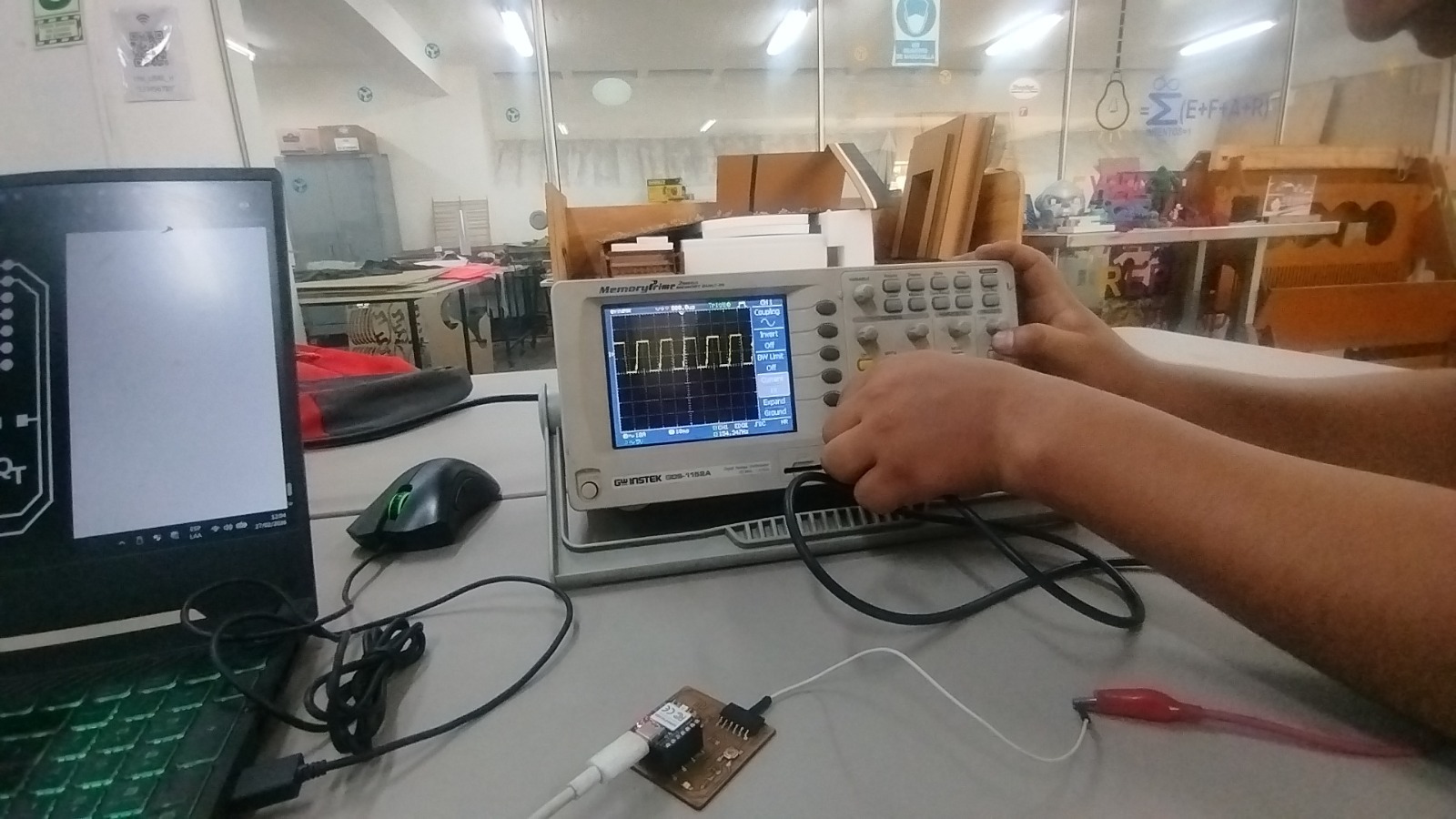
📈4. Results
The oscilloscope displayed a stable and clean square wave signal, which confirmed several important aspects of the system:
- The microcontroller clock and firmware execution were functioning correctly.
- The GPIO output was switching reliably between LOW and HIGH states.
- The board’s power supply remained stable during operation.
🎓5. What We Learned
- How to correctly connect an oscilloscope to an electronic circuit.
- The importance of a solid GND reference for accurate signal measurements.
- The difference between measuring voltage with a multimeter and observing signals with an oscilloscope.
- How real digital signals appear and behave when measured directly in hardware.
Measurement Tool Details
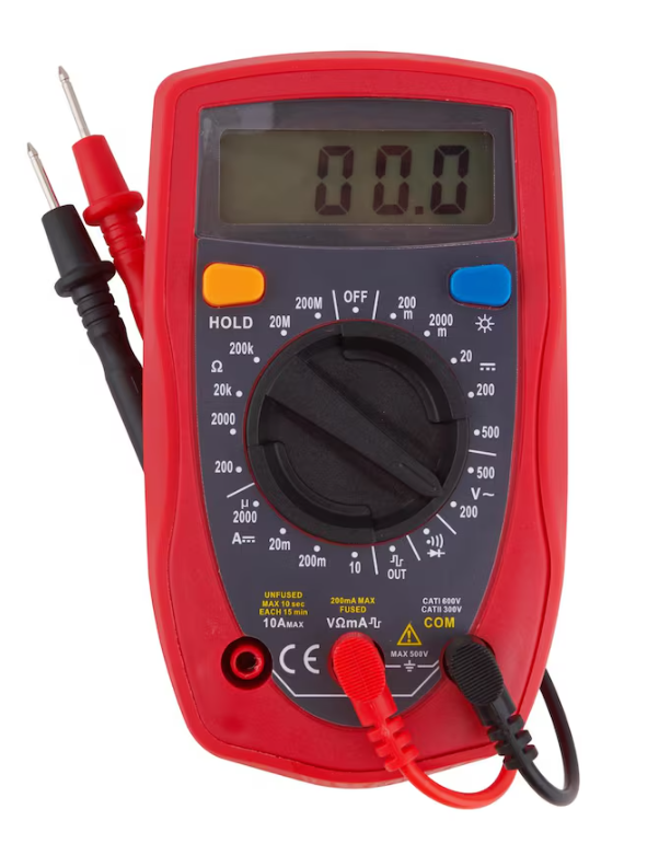
Digital Multimeter (PR-75)
The PR-75 Digital Multimeter is a versatile electronic measuring tool commonly used in laboratories and electronics workshops. It allows technicians and students to verify electrical parameters such as voltage, resistance, and continuity in circuits. This tool is essential for diagnosing basic electrical issues and ensuring that circuits are safe before performing more advanced measurements.
Main Functions:
- Measure DC voltage (3.3V, 5V, etc.).
- Measure AC voltage for alternating current systems.
- Measure resistance (Ω) of electronic components.
- Continuity test with audible beep for detecting short circuits.
- Diode testing for semiconductor verification.
- Measure current (mA / up to 10A) when configured correctly.
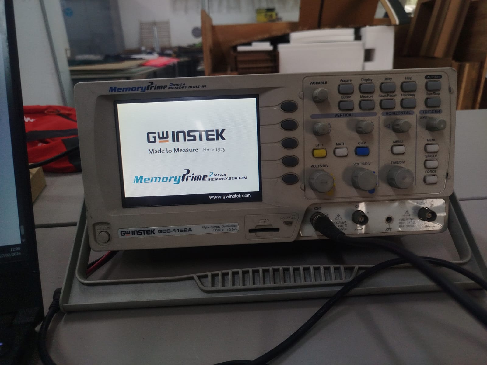
📊Digital Oscilloscope (GW Instek GDS-1152A)
The GW Instek GDS-1152A is a professional digital oscilloscope used to visualize electrical signals over time. Unlike a multimeter, which only displays numerical values, an oscilloscope shows the full waveform of a signal, allowing engineers to analyze signal shape, voltage levels, and timing characteristics.
Main Features:
- Model: GDS-1152A digital oscilloscope.
- Two channels (CH1 / CH2) for comparing signals.
- AUTOSET function for quick automatic configuration.
- VOLTS/DIV control to adjust vertical voltage scaling.
- TIME/DIV control to adjust time base resolution.
- Trigger system for stabilizing waveform visualization.
- Measurement tools for analyzing voltage, frequency, and signal stability.
Difficulties We Faced (Finding the Signal on the Oscilloscope)
At the beginning of the experiment, obtaining a clear and stable waveform on the oscilloscope was not immediate. Several factors affected the measurement process, and we had to troubleshoot different issues before achieving a correct visualization of the signal. The following were the main difficulties we encountered and how we resolved them.
- Incorrect Ground (GND) Connection: Initially, the signal appeared unstable and noisy on the oscilloscope screen. This happened because the ground clamp of the probe was either loosely connected or attached to an incorrect reference point. Once the ground clip was securely connected to the board's main GND pin, the waveform became significantly more stable. Establishing a proper ground reference is essential for accurate signal measurement.
- Probing the Wrong Pin or Test Point: During the first measurements, the probe was connected to a pin that was not configured as the GPIO output in the program. As a result, the oscilloscope did not display the expected waveform. After verifying the microcontroller code and confirming the correct pin label on the board, we repositioned the probe on the correct GPIO output, which allowed us to observe the generated signal.
- Incorrect TIME/DIV and VOLTS/DIV Configuration: Another issue occurred due to improper oscilloscope scaling. When the time base was not correctly configured, the square wave could not properly fit within the display window. After adjusting the time scale to approximately 1 ms/div and fine-tuning the vertical scale to around 1 V/div, the waveform became clearly visible and the voltage transitions between 0 V and 3.3 V could be easily identified.
- Trigger Configuration Problems: Without a proper trigger setting, the waveform continuously moved across the screen, making it difficult to analyze the signal. By enabling the edge trigger on Channel 1 and adjusting the trigger level close to the signal threshold, the waveform stabilized and remained fixed on the display.
- Probe Attenuation Mismatch (x1 / x10): At one point, the voltage values shown on the screen did not correspond to the expected signal amplitude. This was caused by a mismatch between the probe attenuation setting and the oscilloscope channel configuration. After verifying the probe switch and aligning it with the oscilloscope settings, the voltage readings became accurate.
- AUTOSET Limitations: The AUTOSET function helped to quickly generate an initial configuration of the signal display. However, it did not always produce the optimal settings for detailed analysis. Manual adjustments of the time scale, voltage scale, and trigger level were still required to obtain a clean and repeatable waveform.
After correcting the ground connection, confirming the correct GPIO pin, and properly configuring the trigger and oscilloscope scales, we were finally able to observe a clean square wave signal ranging from approximately 0 V to 3.3 V. The waveform appeared stable and matched the timing programmed in the microcontroller, confirming that the system was operating correctly.
Tips and Recommendations (Oscilloscope + Multimeter)
🔎 Multimeter (Before Using the Oscilloscope)
- Check VCC and GND: Measure the voltage between VCC and GND to confirm that the board is receiving the correct power supply (for example around 3.3V).
- Continuity Test: Use the continuity mode to quickly verify that there are no short circuits between VCC and GND.
- Confirm Ground Reference: Make sure the board’s ground pin is clearly identified and accessible before starting measurements.
📡 Oscilloscope (To Find and Stabilize the Signal)
- Always Connect GND First: Attach the probe’s ground clip to the board’s GND before touching the probe tip to the signal pin.
- Start with Safe Scales: Begin with approximate values such as 1 V/div and 1 ms/div, then adjust them until the waveform fits properly on the screen.
- Use Edge Trigger on CH1: Configure the trigger source to Channel 1 (Edge mode) so that the waveform remains stable and easy to read.
- Check Probe Settings (x1/x10): Ensure that the probe attenuation switch matches the oscilloscope channel configuration.
- Use AUTOSET as a Starting Point: The AUTOSET function helps quickly locate the signal, but manual adjustments are usually required for a clear and accurate visualization.
Key Lesson
The most effective workflow is to first use the multimeter to verify that the board is powered correctly and that there are no short circuits. After confirming the electrical safety of the circuit, the oscilloscope can be used to observe the signal by ensuring a proper GND connection, selecting the correct voltage and time scales, and configuring the trigger. Following this sequence allows the square wave signal to be detected and stabilized quickly and reliably.
Individual Assignment
° Use an EDA tool to design a development board that uses parts from the inventory to interact and communicate with an embedded microcontroller
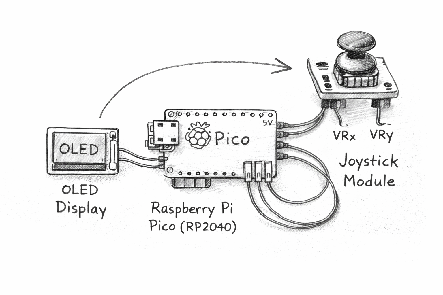
1. Circuit Board Design in KiCad
Raspberry pico-OLED display-Joystick
🔎 1.1 Download and Install KiCad
Go to the official kicad website
🔎1.2 Click on Download and select the version compatible with your operating system (Windows, macOS, or Linux).
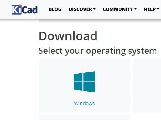
🔎1.3 Download the installer and run the installation file.
🔎1.4 Make sure to install the standard symbol and footprint libraries.
🔎1.5 Once installed, open KiCad .
🔎1.6 verify that the main tools are available: Schematic Editor, PCB Editor, Symbol Editor, and Footprint Editor. .
.png)
2. System Overview
This electronic design is part of my embedded systems exploration and focuses on the development of a small interactive device using a Raspberry Pi Pico (RP2040) microcontroller. The goal of this system is to demonstrate how a microcontroller can read user input and display visual information using simple electronic components.
The device integrates three main components that work together to create a small interactive interface:
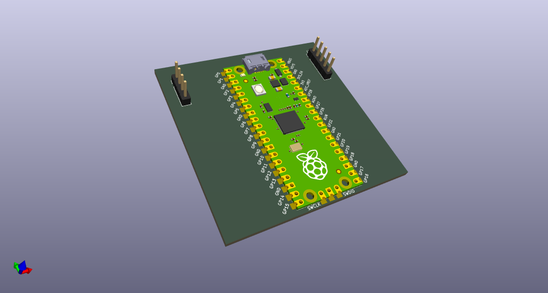
- Raspberry Pi Pico (RP2040) as the main microcontroller responsible for processing inputs and controlling the system.
- OLED Display (128x64) to visualize information in real time, such as graphics, simple animations, or interface elements.
- Joystick Module used as an input device that allows the user to control movement or interact with elements displayed on the screen.
2.1General Operation
The joystick module sends analog signals corresponding to the horizontal and vertical movement of the stick. These signals are read by the Raspberry Pi Pico through its analog input pins (ADC). The microcontroller processes this information and updates the graphics displayed on the OLED screen accordingly.
For example, the joystick can control the movement of an object or cursor on the display, allowing the user to interact with the system in a simple and intuitive way.
2.2Main Purpose of the System
- Understand how microcontrollers process analog input signals.
- Learn how to interface input devices such as a joystick module.
- Display graphical feedback using an OLED screen.
- Explore basic interactive embedded system design.
This initial concept represents the first stage of the system design process, where the overall architecture of the device is defined. From this stage, the project can later evolve into a more complex embedded system with additional sensors, communication modules, or advanced user interfaces.
By integrating user input (joystick) with visual feedback (OLED display), this project demonstrates a fundamental principle of embedded systems: creating interactive devices where hardware and software work together to respond to user actions in real time.
3. Component Selection and Circuit Logic
For this project, I designed a custom development board in KiCad using a Raspberry Pi Pico as the main microcontroller, together with an SSD1306 OLED display and a 5-pin analog joystick module. The Raspberry Pi Pico was selected because it provides multiple GPIO pins, analog inputs, I2C communication support, and a compact design suitable for embedded systems and rapid prototyping. The OLED display was chosen because it offers low power consumption and simple communication through the SDA and SCL pins using the I2C protocol, allowing the microcontroller to display information efficiently while minimizing the number of required connections. Additionally, the analog joystick was integrated using the VRX and VRY pins to provide user input through horizontal and vertical movement detection.
The circuit logic was designed so that the Raspberry Pi Pico receives the analog signals generated by the joystick, processes the input data internally, and then updates the information shown on the OLED display in real time. The system uses both 3.3V and 5V power lines depending on the voltage requirements of the connected components. Through this design, the board combines input and output devices into a single embedded system, allowing interaction between the user and the microcontroller while demonstrating the fundamentals of PCB design, analog signal reading, and digital communication.
4Project: RASPBERRRY PICO + JOYSTICK + OLED Display
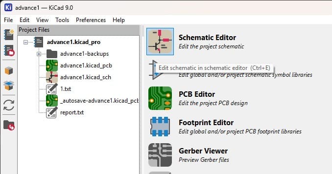
📟4.1 Open the Project and Create the Schematic Sheet
This image shows the main project interface of KiCad. The project includes the schematic and PCB files used to design a custom board based on the Raspberry Pi Pico. The interface provides access to tools such as the Schematic Editor, PCB Editor, and Gerber Viewer for electronic design and fabrication.
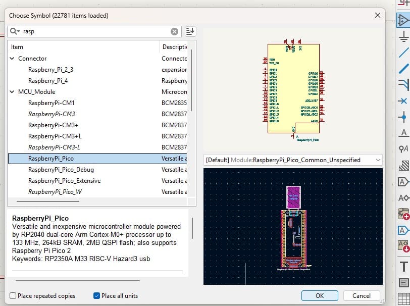
📟4.2 Selecting the components Raspberry Pi Pico, Conn_01x04(Display OLED), Conn_01x05(Joystick) Symbol in KiCad
This image shows the component selection window in KiCad where the schematic symbol for the Raspberry Pi Pico is chosen. The preview displays the pin configuration that will be used when adding the microcontroller to the circuit schematic.
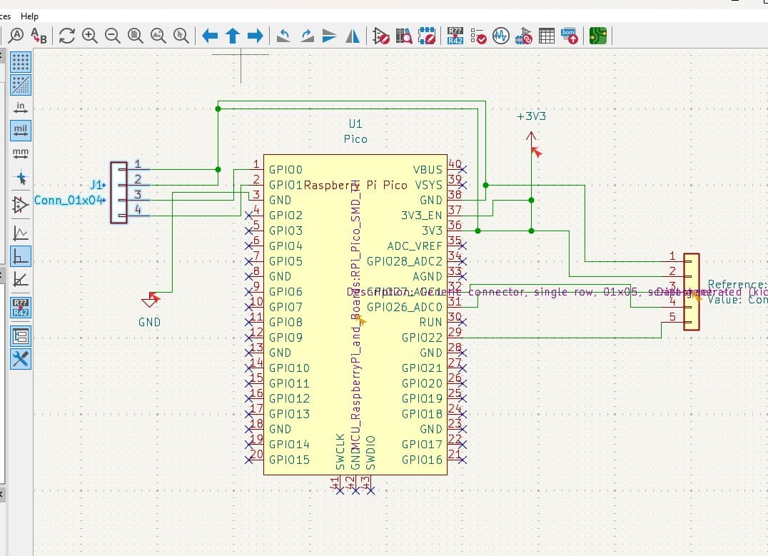
📟4.3 Circuit Schematic with the components Raspberry Pi Pico, Conn_01x04(Display OLED), Conn_01x05(Joystick) Symbol in KiCad
TThis image shows the schematic design created in KiCad using a Raspberry Pi Pico as the main microcontroller. Two pin headers were added to allow connections for GPIO signals, 3.3V power, and GND for external devices.
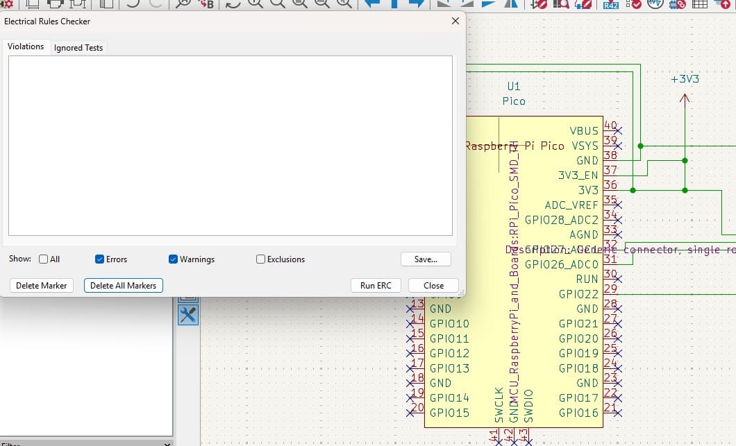
📟5 Schematic Verification with ERC
The Electrical Rules Checker (ERC) tool was executed to verify the schematic. The results show no errors or warnings, confirming that the electrical connections are correctly defined.
📟5.1 Design Rule Validation (ERC & DRC)
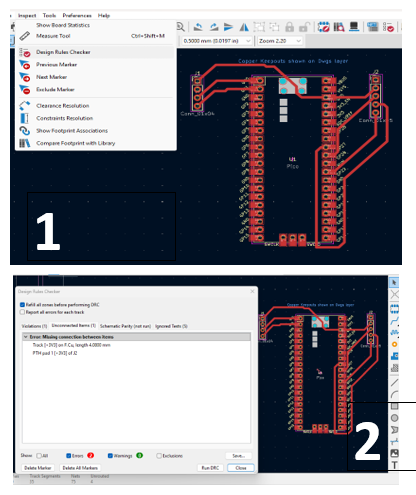
Before finalizing the PCB design, I performed both the Electrical Rule Check (ERC) and the Design Rule Check (DRC) inside KiCad to validate the schematic and PCB layout. The ERC process was used to verify that all the electronic connections in the schematic were correctly configured and that there were no missing or invalid connections between the Raspberry Pi Pico, the OLED display, and the joystick module. This validation step helped ensure that the circuit logic was electrically correct before moving to the PCB manufacturing stage.
After completing the schematic verification, I executed the DRC process to analyze the PCB layout and confirm that the routing parameters followed the design constraints established for the board. The DRC checked important aspects such as trace spacing, clearance values, overlapping tracks, and routing conflicts. Since the PCB was designed as a single-sided board, these validations were especially important to maintain an organized layout and avoid fabrication issues. Both ERC and DRC were completed successfully without critical errors, confirming that the board design was ready for fabrication and electronic production.
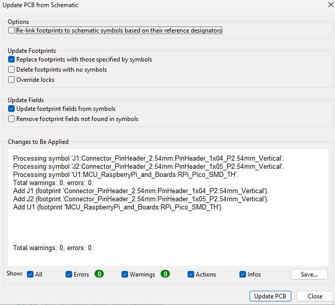
📟5.2 Updating the PCB from the Schematic
The PCB layout was updated from the schematic. During this process, the footprints for the components were assigned and imported into the PCB editor without any errors.
⚙️ 6. Technical PCB Parameters
During the PCB design process in KiCad, different routing parameters were configured to improve the electrical reliability and manufacturability of the board. For the power and ground connections, I used a trace width of 0.8 mm to provide better current distribution and electrical stability across the circuit. For the signal traces connected to the joystick and OLED communication lines, I used a 0.6 mm trace width, which allowed efficient routing while maintaining enough spacing between connections on the PCB. Since the board was designed as a single-sided PCB, maintaining an organized routing structure was important to avoid crossing traces and simplify the fabrication process.
Additionally, I used an approximate clearance value of 0.25 mm between traces and pads to ensure proper electrical isolation and reduce the risk of short circuits during PCB manufacturing. A GND plane was also added to the board design to improve grounding stability, reduce electrical noise, and create a cleaner routing layout. These technical parameters helped create a more reliable PCB design while ensuring that the board could be fabricated correctly and operate safely once assembled.
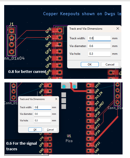
⚙️ Technical PCB Parameters
| 📌 Parameter | 📐 Value | 📝 Description |
|---|---|---|
| Power Trace Width | 0.8 mm | Used for VCC and GND connections to improve current flow and electrical stability. |
| Signal Trace Width | 0.6 mm | Used for communication and analog signal routing such as SDA, SCL, VRX, and VRY. |
| Clearance | 0.25 mm | Minimum spacing between traces and pads to avoid short circuits during fabrication. |
| PCB Type | Single-sided PCB | The board was designed on one copper layer to simplify manufacturing. |
| Ground Plane | Enabled | A GND plane was added to improve grounding stability and reduce electrical noise. |
| Power Supply | 3.3V / 5V | Different voltage levels were used depending on the connected components. |
7. Power Routing Strategy
The power routing of the PCB was organized to provide stable voltage distribution to all the electronic components integrated into the system. The Raspberry Pi Pico acted as the central controller of the board, while the OLED display and joystick module received power through dedicated VCC and GND connections. To improve electrical stability and current flow, wider traces of 0.8 mm were used for the main power and ground lines, while smaller signal traces of 0.6 mm were used for communication and analog input signals.
Special attention was given to organizing the routing paths in order to avoid unnecessary crossing of traces, especially because the PCB was designed as a single-sided board. Additionally, a GND plane was incorporated into the design to improve grounding stability, reduce electrical noise, and create a cleaner PCB layout. Proper power routing was important to ensure reliable communication between the Raspberry Pi Pico, the OLED display using the I2C protocol, and the analog joystick inputs connected through the VRX and VRY pins.
🔋 Power Routing Strategy
| ⚡ Routing Element | Configuration | 📝 Purpose |
|---|---|---|
| Main Power Lines (VCC/GND) | 0.8 mm Trace Width | Used to improve current flow and provide better electrical stability across the PCB. |
| Signal Traces | 0.6 mm Trace Width | Used for SDA, SCL, VRX, and VRY signal routing. |
| Power Supply | 3.3V / 5V | Different voltage levels were distributed depending on component requirements. |
| Ground Plane (GND) | Enabled | Improved grounding stability and reduced electrical noise in the PCB. |
| PCB Type | Single-Sided PCB | Simplified routing and manufacturing process. |
| Routing Organization | Optimized Layout | Reduced unnecessary trace crossings and improved PCB readability. |
| I2C Communication Routing | SDA / SCL Lines | Connected the SSD1306 OLED display to the Raspberry Pi Pico. |
| Analog Input Routing | VRX / VRY Lines | Connected the joystick analog outputs to the microcontroller ADC pins. |
📟8. Component Placement in the PCB Editor
The components were placed in the PCB editor. The visible lines represent airwires, which indicate the electrical connections that need to be routed on the board..
📟9. 3D View of the PCB Design
The 3D viewer was used to visualize the final PCB design. This allows verification of the component placement and the overall appearance of the board before manufacturing.
📟 10. Difficulties (Individual)
During the development of this project, one of the main difficulties was adapting to the electronic design software, since the interface and workflow were new to me. I spent time searching through the libraries to find the correct symbols and footprints for the Raspberry Pi Pico, the OLED display,and the joystick, making sure the pin configurations matched the real components.
Another challenge appeared during the PCB layout stage, where I had to carefully organize the components and route the traces correctly. I realized that the placement of the Raspberry Pi Pico, the OLED display, and the joystick is essential to achieve a clean and functional board design. This process helped me better understand how to optimize space and improve the circuit layout.
📟11. Individual Assignment Reflection
This assignment helped me better understand the complete electronics design workflow, from schematic creation to PCB layout preparation using KiCad. By designing a custom development board that integrates a Raspberry Pi Pico, a joystick, and an OLED display, I learned how electronic components communicate with a microcontroller and how proper routing, pin organization, and component placement are essential for a functional board design. I also improved my understanding of electronic design constraints, circuit organization, and the importance of planning both the electrical connections and the physical arrangement of the components before fabrication.
Files
Here are the project files available for download:
- KiCad Board 9.0: Download .pcb
- KiCad Project 9.0: Download .pro
- KiCad Schematic 9.0: Download .sch
- 3D View: Download .png