Electronics Production.
Week 08 — Electronics Production.
weekly schedule.
| Time block | Wed | Thu | Fri | Sat | Sun | Mon | Tue | Wed |
|---|---|---|---|---|---|---|---|---|
| Global class | 3 h | |||||||
| Local class | 1,5 h | |||||||
| Research | ||||||||
| Design | 3 h | 2 h | ||||||
| Fabrication | 2 h | 4 h | ||||||
| Documentation | 2 h | 2 h | 4 h | 3 h | ||||
| Review |
overview.
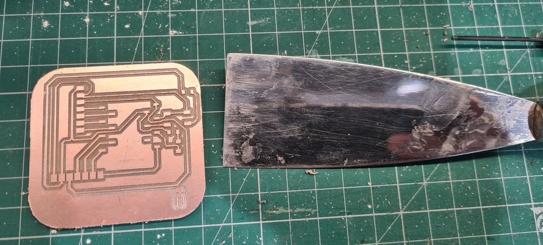
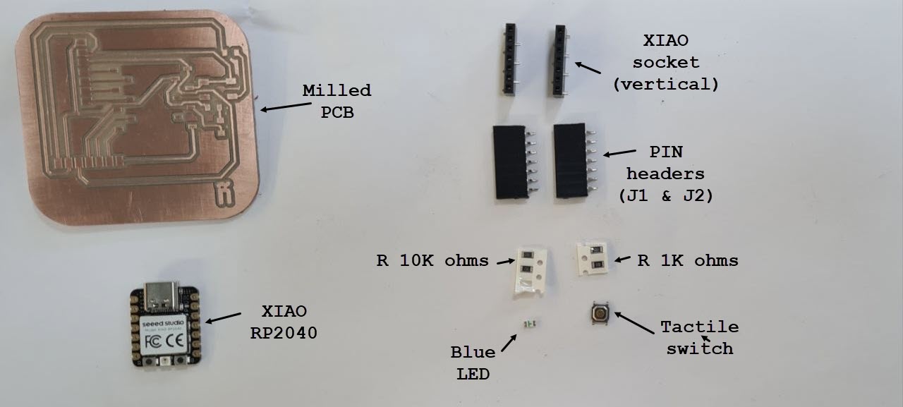
This week is about taking a PCB design from files to a physical, functional board. The workflow covers toolpath generation, milling on the Roland MDX-20, soldering SMD and through-hole components, and verifying the board works. The board I’m producing is the one I designed during Week 06 — a breakout board for the XIAO RP2040 — with a significant redesign pass that happened this week before sending it to the mill.
learning objectives.
- Describe the process of tool-path generation, milling/laser engraving, stuffing, de-bugging and programming.
- Demonstrate correct workflows and identify areas for improvement if required.
assignments.
- Group assignment:
- characterise the design rules of the in-house PCB production process (Roland MDX-20).
- document the workflow for sending a design to an external boardhouse.
- document your work to the group work page and reflect on your individual page what you learned.
- Individual assignment:
- Make and test a microcontroller development board that you designed.
group assignment.
The group assignment for this week covers two things: characterising the design rules of our in-house PCB production process (the Roland MDX-20), and documenting the workflow for sending a PCB to a boardhouse. Both are documented here and on the Fab Lab León 2026 Group Page.
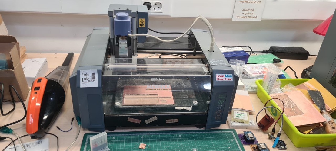
roland MDX-20 — machine characterisation.
The Roland MDX-20 is a small desktop CNC mill used exclusively for PCB fabrication in our lab. It works by physically removing copper from a copper-clad FR1 board using carbide end mills, following toolpaths generated by mods.
Tooling and parameters used:
| Parameter | Traces | Cutout |
|---|---|---|
| Tool | 1/64” flat end mill | 1/32” flat end mill |
| Diameter | 0.0156 in | 0.0312 in |
| Cut depth | 0.0040 in | 0.0240 in |
| Max depth | 0.0040 in | 0.0720 in |
| Speed | 2 mm/s | 2 mm/s |
| Offsets | 4 | 1 |
| Stepover | 0.5 | — |
Toolpath parameters are taken directly from the mods CE node configuration used during the milling session.
The trace mill makes four offset passes around each trace to clear enough copper. The cutout mill cuts through the board perimeter in three passes (max depth 0.0720 in ÷ 0.0240 in per pass).
Design rules derived from characterisation:
- Minimum trace width: 0.4 mm (recommended ≥ 0.4 mm to survive milling)
- Minimum clearance: 0.4 mm
- Minimum drill size: not applicable (no mechanical drilling — use through-hole pads as reference only)
- Board material: single-sided copper-clad FR1
Design rule values follow the Fab Academy standard for the Roland MDX-20 with a 1/64” end mill, consistent with the parameters set by our instructor.
sending to an external boardhouse.
For reference, here is an overview of the main options when sending Gerbers to a professional PCB manufacturer — relevant when the board requires tolerances or finishes that a desktop mill can’t produce. The in-house milling workflow is documented in the toolpath generation section. We went through the full ordering process with this board as a reference exercise using JLCPCB.
Sending to JLCPCB — step by step.
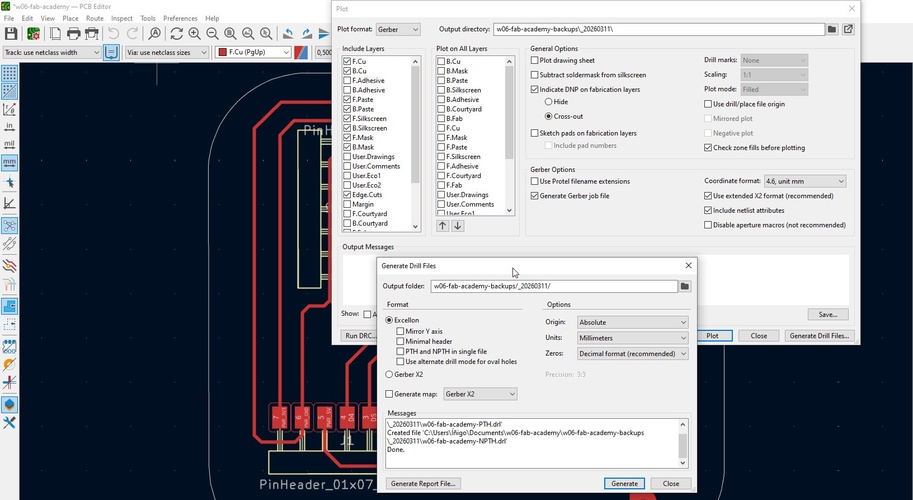
1. Export Gerbers from KiCad. In the PCB Editor: File → Fabrication Outputs → Gerbers → Plot. We select all required layers — F.Cu, B.Cu, F.Silkscreen, F.Mask, Edge.Cuts — and generate the drill files from the same dialog (Generate Drill Files → Generate). The output folder gets zipped and that ZIP is what we upload to JLCPCB.
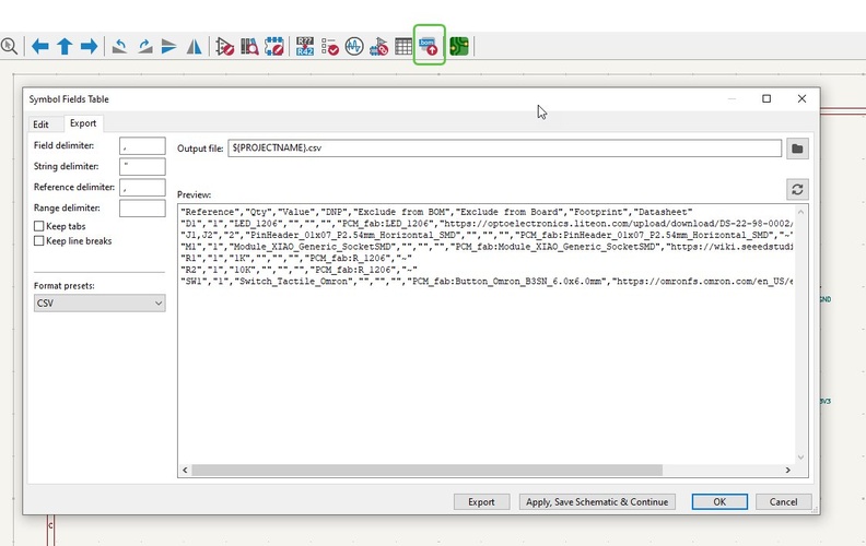
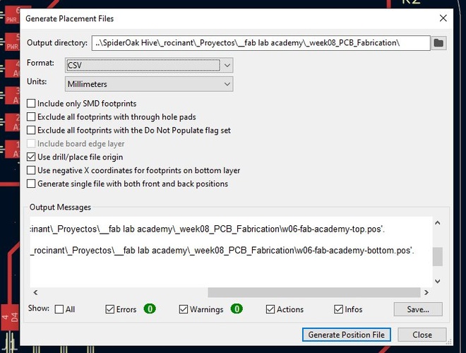
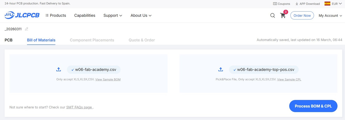
2. Export the BOM and CPL. JLCPCB requires two files for PCB assembly (PCBA): a Bill of Materials (BOM) and a Component Placement List (CPL, also called Pick & Place file). We generate both from KiCad now — we will need them later in the process when JLCPCB asks for them before component matching. For the BOM: in the Schematic Editor, go to Tools → Edit Symbol Fields → Export tab. Output format CSV. For the CPL: in the PCB Editor, go to File → Fabrication Outputs → Component Placement (.pos). Set format to CSV and units to Millimeters. Click Generate Position File. KiCad outputs two files — top and bottom — we use the top one.
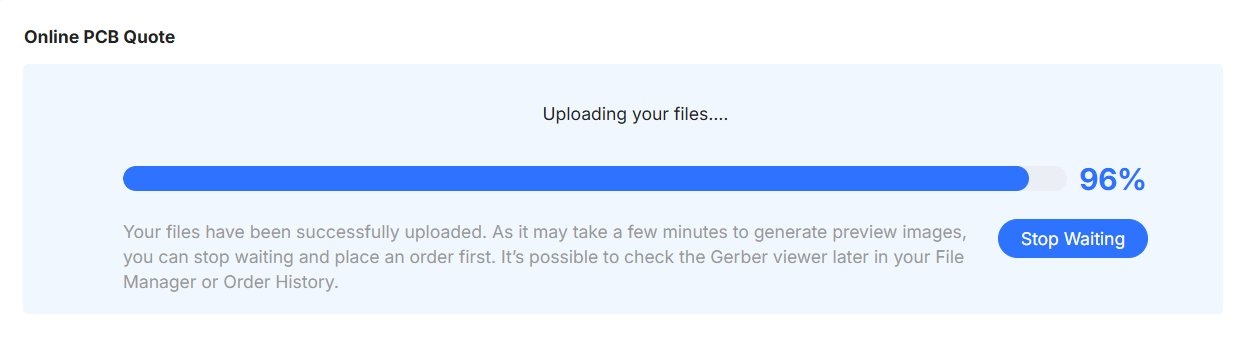
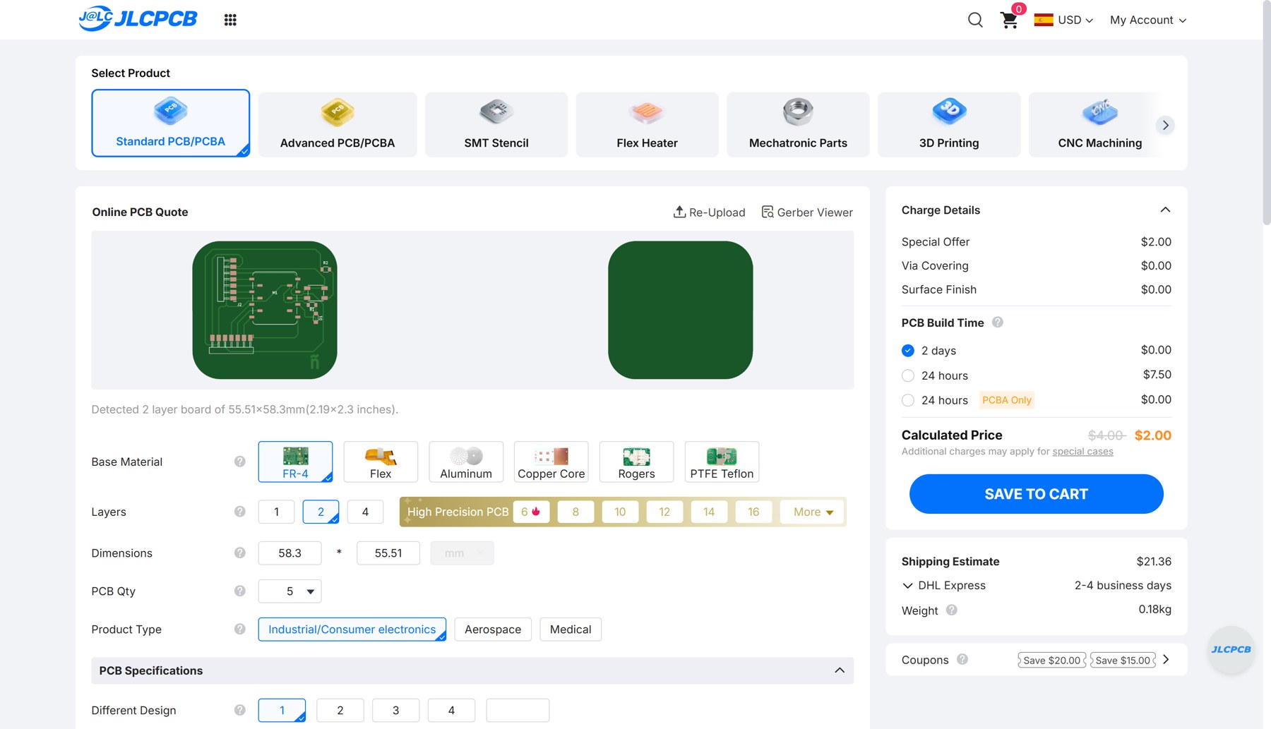
3. Upload Gerbers and configure the order. We go to jlcpcb.com, click Order Now, and drag the Gerber ZIP into the upload field. JLCPCB parses the files and pre-fills most parameters automatically. The upload progress screen notes that Gerber preview generation may take a few minutes — we can configure the order while waiting.
Once parsed, we verify base material (FR-4), 2 layers, 1.6 mm thickness, green solder mask, HASL finish, and quantity. Worth checking the Mark on PCB option: by default it is set to Order Number, which prints a reference code on the board. We set it to Remove Mark to keep the silkscreen clean. The integrated PCB viewer shows a 3D render of the board — we use this to confirm the outline parsed correctly and no layers are missing.
4. Sign in and proceed. After configuring the order and clicking Next, JLCPCB asks us to sign in before proceeding to checkout.

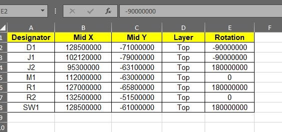
5. Upload BOM and CPL. Once signed in, JLCPCB asks for the BOM and CPL files we generated in step 2. Here is where the format issue appears: the CSV files exported by KiCad are rejected by the uploader — the column headers don’t match what the platform expects. The workaround is to download JLCPCB’s sample XLS templates (links available on the BOM and CPL upload panels) and manually copy the values into the correct columns. The CPL requires at minimum: Designator, Mid X, Mid Y, Layer, Rotation.
With both files reformatted and uploaded, each shows a green checkmark. We click Process BOM & CPL to continue.
6. Component matching. After processing, JLCPCB shows a component matching screen. It auto-matches what it can from its parts library — D1 (LED 1206), R1 (1 KΩ), and R2 (10 KΩ) are matched to specific stock parts. J1/J2 (pin headers), M1 (XIAO socket), and SW1 (tactile switch) appear as unmatched: they use Fab Lab-specific footprints that don’t map to standard JLCPCB inventory.
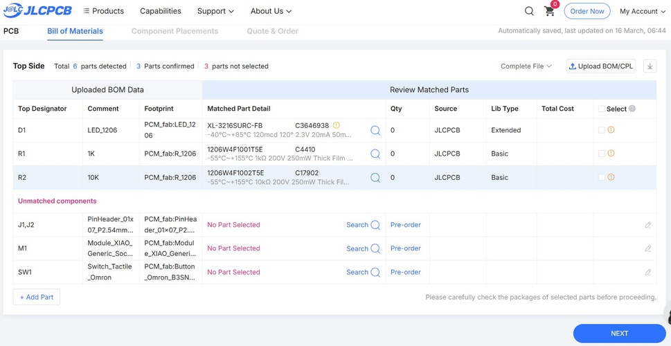
For the unmatched components there are two options: use the Search tool within JLCPCB to find an equivalent part in their catalogue, or mark them as Pre-order and source them separately. For this board — which uses a Seeed XIAO RP2040 module and Fab-specific SMD connectors — the XIAO socket and headers are not standard JLCPCB stock items and would need to be pre-ordered or hand-assembled after delivery. This is the normal situation for boards designed with non-commodity modules: the passive components assemble fine through JLCPCB PCBA, but anything Fab-specific or module-based requires a separate sourcing step.
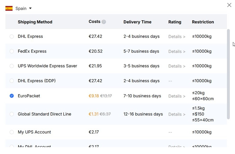
7. Shipping and VAT. We select EuroPacket for Spain (€9.18, 7–10 business days). At checkout, JLCPCB offers to pre-collect the 21% Spanish VAT — we select this to avoid surprises at customs.
A note on intellectual property. When we upload Gerber files to JLCPCB or any similar service, we are sending our full board design to a third party with no NDA or confidentiality agreement in place by default. For a Fab Academy exercise board this is not a concern, but it is worth keeping in mind for any design that contains genuinely novel work or proprietary circuitry. If that is the case, an EU-based manufacturer like Eurocircuits or Aisler — where at least the legal framework is clearer and closer — may be worth the price difference. For anything truly sensitive, a signed NDA with the manufacturer before submitting files is the only real protection.
🤖 Claude (Anthropic) on the boardhouse comparison prompt:
Compare the main PCB prototype manufacturers available for a hobbyist or Fab Academy student ordering from Spain. Include only manufacturers with a realistic track record in the maker/open hardware community. For each one, provide: location, brief notes on quality and service, and an approximate price breakdown for a 60×40 mm, 2-layer, green, HASL, FR4 1.6 mm board — 5 and 10 units — shipped to Spain, with VAT and customs considerations. Sort by total cost ascending. Flag any known issues with quality, customs friction, or community reputation.
Note: VAT applies to all EU imports regardless of value. The €150 threshold is for customs duties only, not VAT. Reflect this accurately in the customs column.
| Manufacturer | Location | Notes |
|---|---|---|
| Eurocircuits | Belgium / Germany / Hungary | Fabrication within EU. High quality, thorough DFM checks, higher price point. Best option when lead time is critical or customs friction must be avoided. |
| Aisler | Netherlands | EU-based, accepts KiCad files directly, stencils available. Quality and support have been inconsistent according to community reports. |
| JLCPCB | China (EU rerouting via Luxembourg) | Cheapest option. Ships to EU via a remailer to avoid import duties on small orders. 5 boards from ~$2. Lead-free finish available. |
| PCBWay | China | Slightly more expensive than JLCPCB, but reviewed favourably for quality and DFM communication. |
| Elecrow | China | Similar price range to JLCPCB. Good quality track record among makers. |
For price comparison across all these services before ordering, PCBShopper is a useful aggregator. A note on EU customs: orders from China below ~150 € are subject to VAT at import. JLCPCB offers pre-paid VAT at checkout to avoid surprises at customs.
Approximate price comparison — 60×40 mm board, 2 layers, green, HASL, FR4 1.6 mm, shipped to Spain.
All prices in euros, indicative only. Check each manufacturer’s calculator for exact quotes at time of order.
| Manufacturer | 5 boards (fab) | 5 boards (shipping) | VAT / customs | 5 boards total | 10 boards total | Lead time |
|---|---|---|---|---|---|---|
| JLCPCB | ~2 € | ~6 € (EuroPacket) | 21% VAT prepayable at checkout | ~10 € | ~10 € | 7–12 days |
| Elecrow | ~5 € | ~15 € (DHL) | 21% VAT at customs | ~24 € | ~24 € | 10–15 days |
| PCBWay | ~5 € | ~18 € (DHL) | 21% VAT at customs | ~28 € | ~29 € | 7–12 days |
| Aisler | ~20–30 € | ~6 € (intra-EU) | Included (intra-EU) | ~28–38 € | ~33–43 € | 5–7 working days |
| Eurocircuits | ~35–45 € | ~8 € (intra-EU) | Included (intra-EU) | ~45–55 € | ~50–65 € | 3–5 working days |
A few things worth noting. JLCPCB’s $2 fabrication price covers any board under 100×100 mm regardless of quantity — so 5 and 10 units cost the same to make, and only the shipping weight changes. The gap between Chinese and European manufacturers is real and significant for hobbyist runs; Eurocircuits is roughly 5× more expensive than JLCPCB for the same board, but comes with no customs friction, a proper EU invoice, and 3–5 day turnaround from Germany or Hungary. Aisler is theoretically competitive on price but has a mixed reputation for quality in recent community reports — worth checking current reviews before ordering.
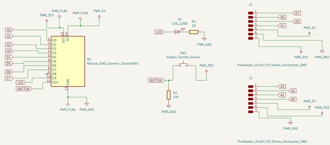
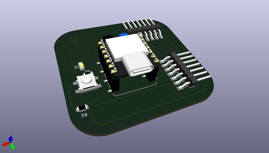
PCB design — redesign from week 06.
The board I designed in Week 06 was functional but minimal: a XIAO RP2040 socket with an LED, a button, and two resistors. Before milling it, Adrián (our instructor this week) suggested making it more versatile by adding expansion headers, so the board can interface with external circuits or be used as a base for future projects.
what changed.
Added two 1×7 pin headers, one on each side of the board (J1 and J2), both in horizontal SMD format. The decision to go horizontal rather than vertical was Adrián’s suggestion — horizontal headers sit flush against the board edge and are mechanically more stable when connectors are plugged and unplugged.
Each header exposes the following signals, by design:
- J1: D4, D5, D6, D7 + 5V, 3.3V, GND
- J2: A0, A1, A2, A3 + 5V, 3.3V, GND
The convention of always reserving one pin per rail (GND, 5V, 3.3V) on every header is a habit worth building early. It makes the board self-sufficient for powering peripherals without requiring separate wiring.
Pin assignment following the XIAO’s intended functionality.
Adrián also pointed out that the pin assignment should respect how the XIAO RP2040 pins are originally conceived. The first four pins (A0–A3) are the dedicated analog inputs, so they go to J2 — keeping that header for analog-capable signals. The next group (D4–D7) includes the SPI bus pins, so they go to J1, keeping communication-capable pins together on one side. The LED and the button are connected to general-purpose digital pins that are neither analog, nor SPI, nor UART — so they don’t occupy pins that might be needed later for those protocols. It’s a small thing, but it makes the board more predictable to work with: if you know where to look for analog or SPI signals, you don’t have to read the schematic every time.
Corrected the button circuit. In the original design the pull-down resistor for the tactile switch wasn’t wired correctly — it was effectively acting as a pull-up. This was fixed. R2 (10 KΩ) is now correctly connected between the BUTTON net and GND, pulling the pin low when the button is open.
The value of 10 KΩ is not arbitrary. The rule of thumb is that the pull-down resistor should be roughly one tenth of the input pin’s impedance, which on CMOS microcontrollers is typically in the range of 100 KΩ. At 10 KΩ, the resistor defines a stable low level (≈ 0 V) when the button is open, while only drawing 3.3 V / 10 KΩ = 330 µA to ground when the button is pressed — an acceptable steady-state current. Going higher (e.g. 1 MΩ) risks a floating or noise-sensitive input; going lower (e.g. 100 Ω) wastes current unnecessarily.
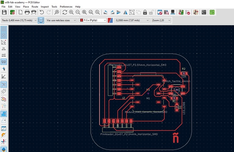
Routing iterations. Adding the two headers created significant routing complexity. The pin assignment inside each header went through several iterations — I had to rearrange which signal went to which pin multiple times because KiCad’s PCB Editor was generating crossing ratsnests that couldn’t be resolved cleanly. Each time I moved a component that already had routes, the existing tracks didn’t follow coherently, which meant deleting and rerouting segments one by one. It’s the main friction point in KiCad’s PCB Editor: there’s no push-and-shove routing for already-placed tracks when you move a footprint.
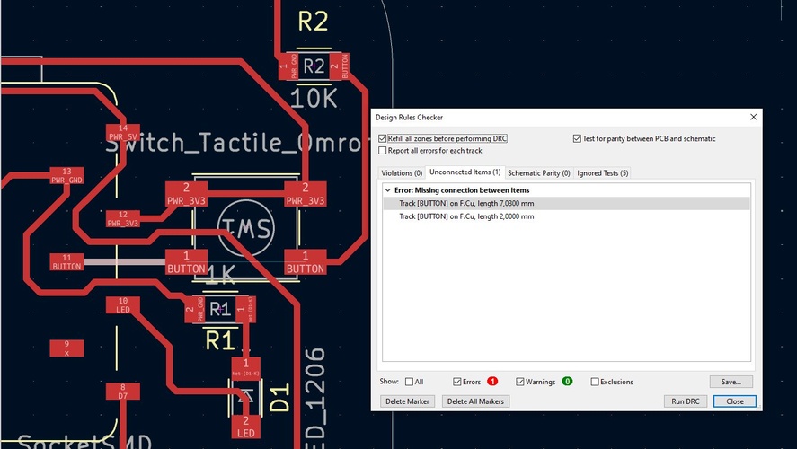
The BUTTON unconnected item. When running the DRC, there’s one persistent Unconnected Items error: the two pads of SW1 that correspond to the BUTTON net on F.Cu. Adrián helped resolve the routing deadlock by adjusting the button’s position and removing the explicit track between SW1’s two terminals, since the switch internally connects them. The DRC reports this as a missing connection, but electrically it’s not a problem — the button works as intended. It’s a known and accepted deviation.
KiCad layer reference.
KiCad’s layer system was one of the things that confused me most during the design phase — there are dozens of layers visible in the interface and it’s not obvious at first which ones actually matter for fabrication and which are purely informational. I’m documenting this here as a reference to come back to.
KiCad organises the PCB design into stacked layers, each with a specific role in the fabrication process. These are the layers relevant to a single-sided board milled at Fab Lab León:
| Layer | Type | Purpose |
|---|---|---|
| F.Cu | Copper | Front copper layer — traces, pads, and all copper features on the top face |
| B.Cu | Copper | Back copper layer — not used on single-sided boards |
| F.Silkscreen | Silkscreen | White ink on the front face — labels, logos, text. Not produced by milling |
| B.Silkscreen | Silkscreen | Same, on the back face |
| F.Mask | Solder mask | Protective coating (usually green) that covers copper except at pad openings. Not produced by milling |
| B.Mask | Solder mask | Same, on the back face |
| F.Courtyard | Mechanical | Minimum keep-out boundary around each component — used by DRC to detect collisions |
| F.Fab | Documentation | Assembly reference layer — component outlines and pin 1 markers |
| Edge.Cuts | Mechanical | Board outline — defines the shape that will be cut out. Must be a single closed path |
| User.Eco1 / Eco2 | User-defined | Free layers for notes, milling guides, or any non-fabrication markup |
For PCB milling on the Roland MDX-20, only two layers produce physical output: F.Cu (isolation milling, 1/64” endmill) and Edge.Cuts (contour cut, 1/32” endmill). Everything else is either irrelevant for milling or used only for DRC checks and documentation inside KiCad.
schematic.
PCB layout.
DRC result.
3D preview.
interactive BOM.
The plugin InteractiveHtmlBom for KiCad generates a self-contained HTML file that links each component in the BOM to its location on the board. Useful for assembly.
Open Interactive BOM in new tab ↗
Bill of Materials:
| Reference | Value | Footprint | Qty |
|---|---|---|---|
| M1 | XIAO RP2040 | Module_XIAO_Generic_SocketSMD | 1 |
| J1, J2 | Pin Header 1×7 | PinHeader_01x07_P2.54mm_Horizontal_SMD | 2 |
| SW1 | Switch_Tactile_Omron | SW_SPST_PTS645 | 1 |
| D1 | LED_1206 | LED_1206_3216Metric | 1 |
| R1 | 1 KΩ | R_1206_3216Metric | 1 |
| R2 | 10 KΩ | R_1206_3216Metric | 1 |
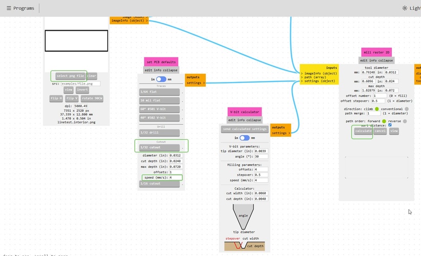
toolpath generation — mods.
mods is a browser-based CAM tool developed within the Fab Academy network. It works as a node graph: you connect processing blocks together to define the full pipeline from input image to machine file. We could think of it as a slicer for CNC milling — but instead of an STL and a layer-by-layer approach, it takes a PNG image (black and white, no greyscale) and generates toolpaths by reading the pixel geometry directly.
The workflow starts from PNG exports of the Gerber layers, not from the Gerbers directly. The machine connection uses the Web Serial API, which requires a Chromium-based browser. In my case, Chrome is the chosen browser for the full workflow — both toolpath generation and live machine connection via WebSerial. Chromium (the open-source build, without Google telemetry) is a valid privacy-respecting alternative that also supports Web Serial API fully. I had compatibility issues with other browsers in Week 06 — see the note in that week’s documentation for details.
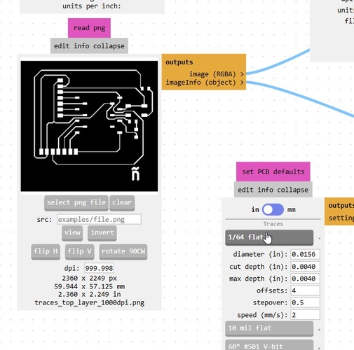
exporting PNGs from KiCad.
In KiCad’s PCB Editor: File → Fabrication Outputs → Gerbers → Plot. This generates the Gerber files. Then, back in mods, these are not used directly — instead, use a dedicated Gerber-to-PNG converter (Gerber2Png or the KiCad built-in plot to PNG at 1000 dpi) to get the two images needed:
traces_top_layer_1000dpi.png— copper traces (white on black)outline_top_layer_1000dpi.png— board outline for the cutout
A note on SVG export. KiCad can also export SVG files for each layer, and older versions of mods handled them well. Currently this is not reliable — KiCad’s SVG output includes artefacts (stray lines, malformed paths) that confuse the mods toolpath generator and can produce erratic mill behaviour. Stick to PNG. The format must be strictly black and white — no greyscale, no anti-aliasing. If the image has intermediate grey values, mods will misinterpret the threshold and generate incorrect paths.
full workflow: KiCad → mods → Roland MDX-20.
My complete process from a finished KiCad design to a milled board:
- Finish routing in the KiCad PCB Editor. Run DRC and resolve all violations — in my case, the one known exception (BUTTON unconnected item) is accepted and documented.
- Export Gerbers: File → Fabrication Outputs → Gerbers → Plot. I need F.Cu and Edge.Cuts as a minimum. I also generate drill files from the same dialog (Generate Drill Files → Generate), even though the Roland MDX-20 doesn’t use them for drilling.
- Convert Gerbers to PNG at 1000 dpi — I use Gerber2Png or KiCad’s built-in plot-to-PNG. Two files: traces (F.Cu, white on black) and board outline (Edge.Cuts).
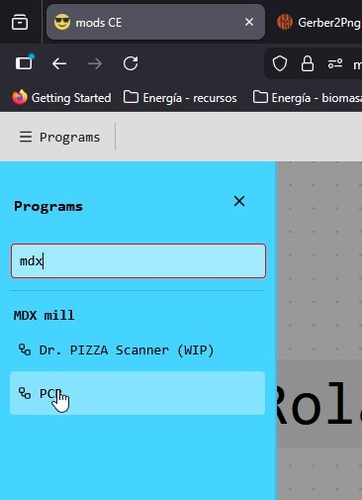
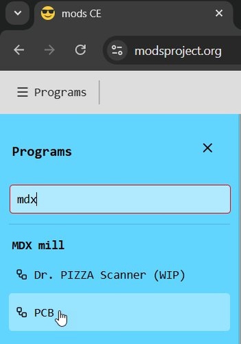
- Open modsproject.org in Chrome or Chromium. Go to Programs → type
mdx→ select MDX mill → PCB. This loads the full node graph. - Load the traces PNG into the read png node. Set tool to 1/64 flat, speed 2 mm/s, offsets 4. Calculate and check the simulation view before sending anything.
- Open a new session for the outline PNG. Switch to 1/32 cutout, speed 2 mm/s. Calculate and verify again.
- On the Roland MDX-20: tape down the copper-clad board, set XY origin with the jog controls, probe Z. Run the traces job first, then swap the tool and run the cutout.
mods setup.
I open modsproject.org in Chrome or Chromium — the Web Serial API needs a Chromium-based browser to talk directly to the machine. Click the hamburger menu → Programs → type mdx → select MDX mill → PCB. This loads the full node graph.
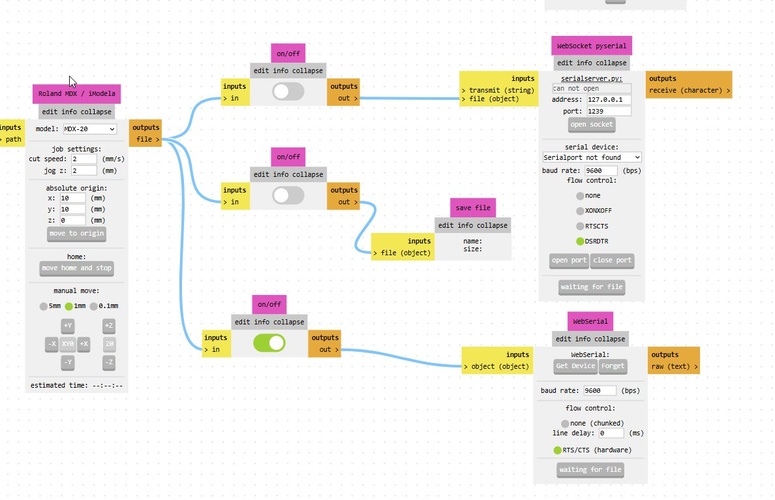
traces toolpath.
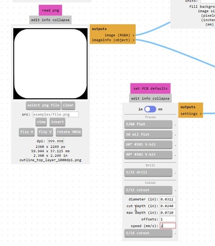
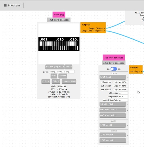
Load traces_top_layer_1000dpi.png into the read png node. The image dimensions are read automatically (2360 × 2249 px, 59.944 × 57.125 mm).
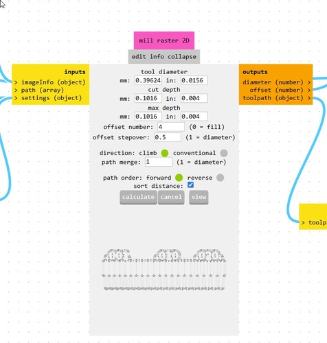
Key settings in the set PCB defaults node for traces:
- Tool: 1/64 flat
- Diameter: 0.0156 in
- Cut depth: 0.0040 in
- Max depth: 0.0040 in
- Offsets: 4
- Stepover: 0.5
- Speed: 2 mm/s
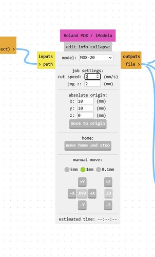
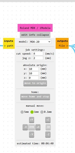
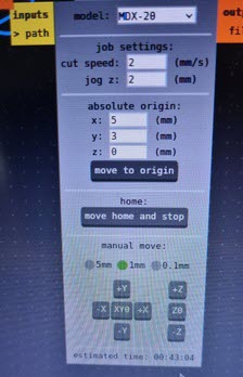
In the Roland MDX / iModela node, set model to MDX-20, cut speed to 2 mm/s, jog Z to 2 mm. The absolute origin (X: 5, Y: 3, Z: 0) defines where on the physical board the job starts — set on the machine before running.
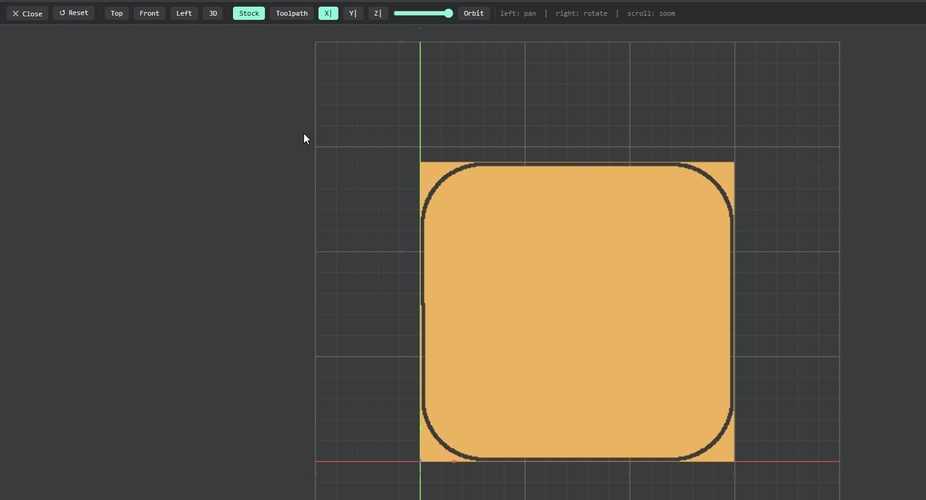
cutout toolpath.
Load outline_top_layer_1000dpi.png into a new session (or reload mods with the same program). Switch to the 1/32 cutout tool:
- Diameter: 0.0312 in
- Cut depth: 0.0240 in
- Max depth: 0.0720 in (three passes)
- Offsets: 1
- Speed: 2 mm/s
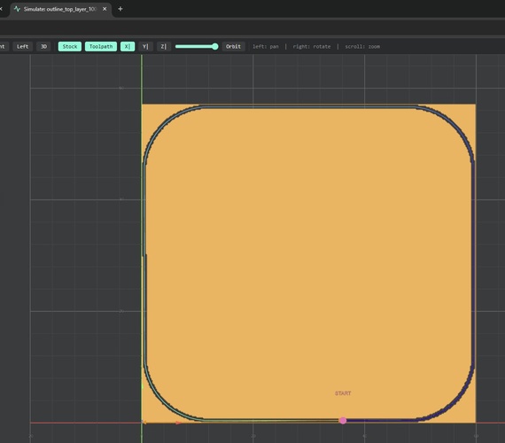
toolpath verification.
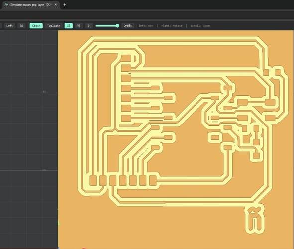
Before sending anything to the machine, it’s worth spending two minutes in the simulation view. The traces toolpath should show clean, merged isolation channels — each trace surrounded by a consistent copper-free gap, with no isolated islands or disconnected segments. If you see a trace that looks unrouted or a pad with no clearance around it, something is wrong with either the PNG export or the tool diameter setting.
What the simulation catches that DRC misses: DRC validates the KiCad design against electrical rules, but it knows nothing about what the 1/64” endmill can physically fit between. A 0.3 mm clearance between two traces will pass DRC (if the minimum was set loosely) and fail silently in the mill — the tool simply won’t fit and will leave a copper bridge. The simulation makes this visible.
One practical fix that came up: minor PNG export artefacts — stray pixels at the board edge, a slightly closed gap — can be corrected in GIMP or any other raster graphics editor before sending to mods. Open the PNG, use the pencil tool at 1–2 px with pure black or white, fix the pixel, export as PNG (no compression, strictly B&W). It takes less time than rerunning the full export chain.
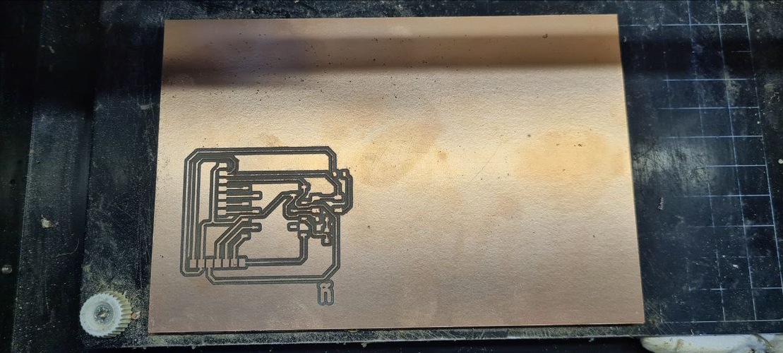
The estimated milling time for this board was 43 minutes (shown in the mods MDX-20 node), which matches the actual trace milling run.
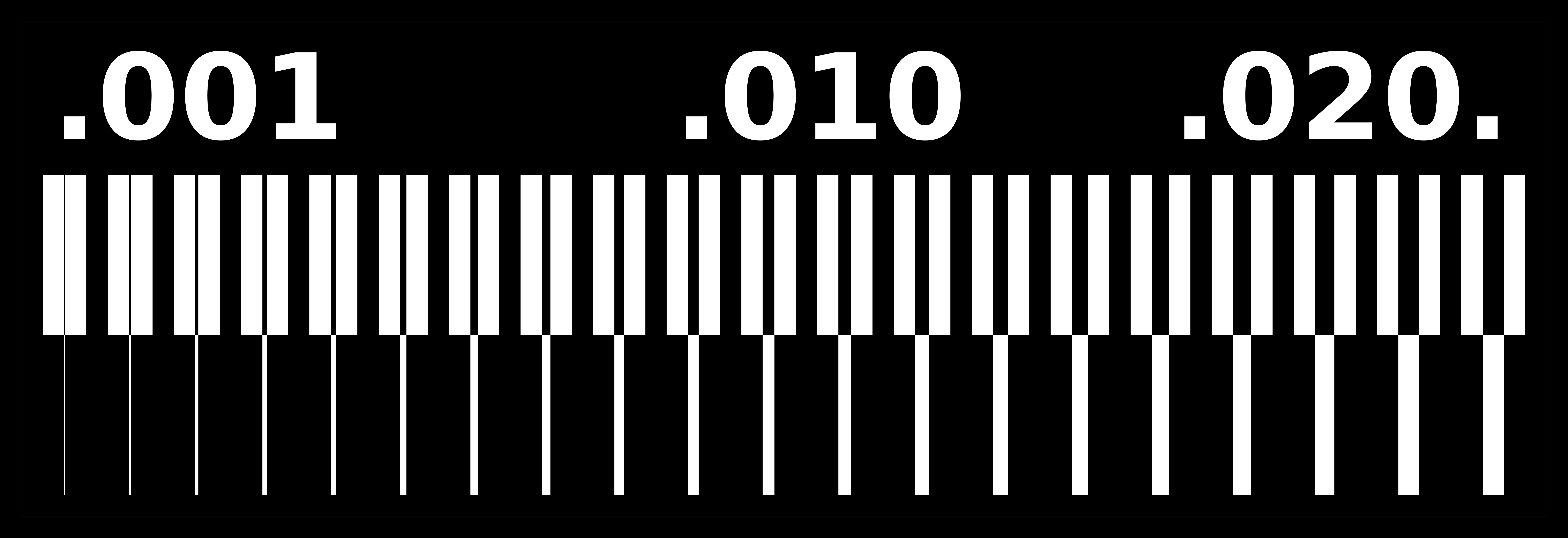
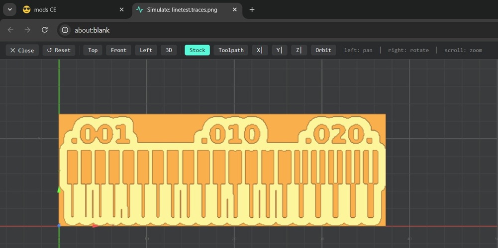
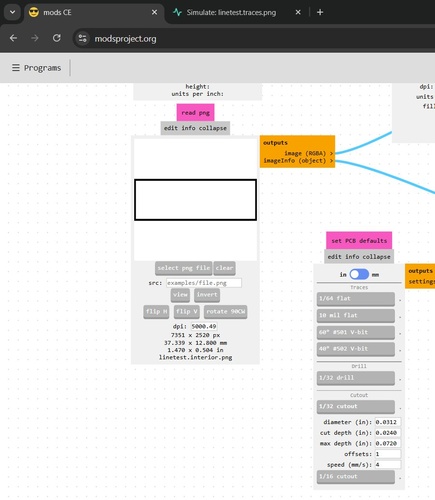
line test — characterising the MDX-20.
The steps below walk through milling the Fab Academy line test — the standard file used to characterise the MDX-20’s trace resolution at three different clearance values: 0.001, 0.010, and 0.020 inches. I’m going through this to document the full workflow: preparing the file, configuring the toolpath in mods, and setting up the machine.

Traces toolpath.
I open modsproject.org in Chrome, go to Programs → type mdx → select MDX mill → PCB.
Cutout toolpath.
Once the traces job is done I open a new mods session with the same program, load the outline PNG, and switch to the 1/32 cutout tool.
After verifying the toolpath simulation and confirming the WebSerial connection, I send both jobs to the machine. The result:

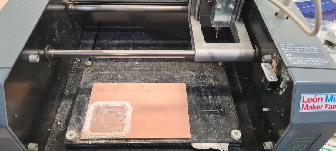
milling.
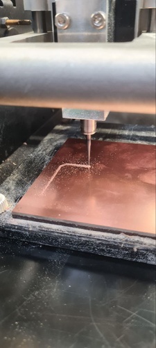
The milling session happened at Fab Lab León with Adrián’s supervision. The full process from raw copper-clad board to milled PCB takes roughly an hour end to end, split between preparation, traces job (43 minutes), tool change, and cutout.
preparing the board.
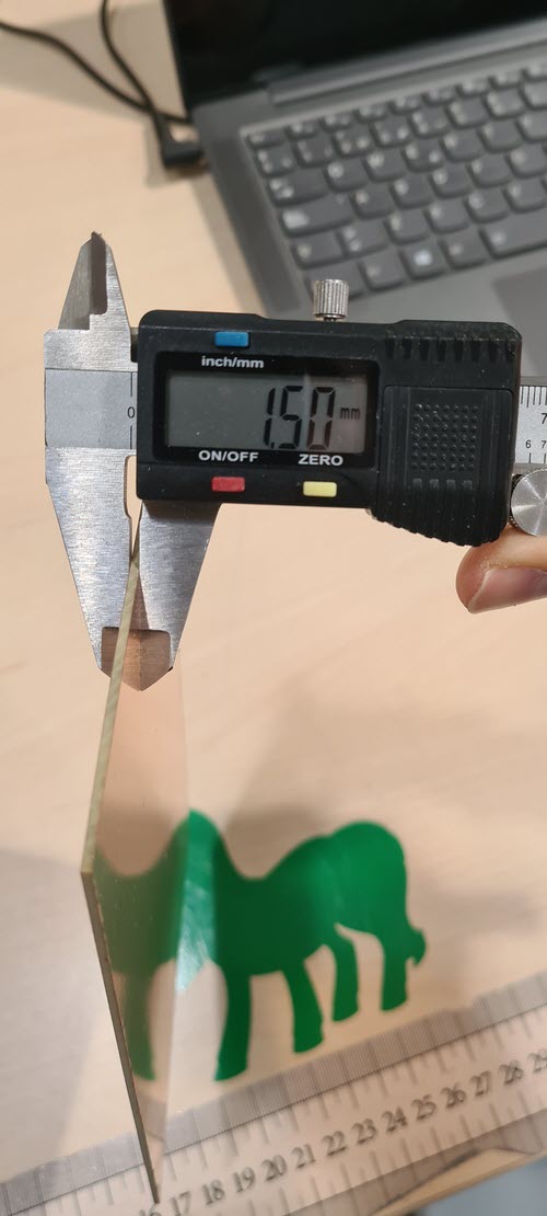
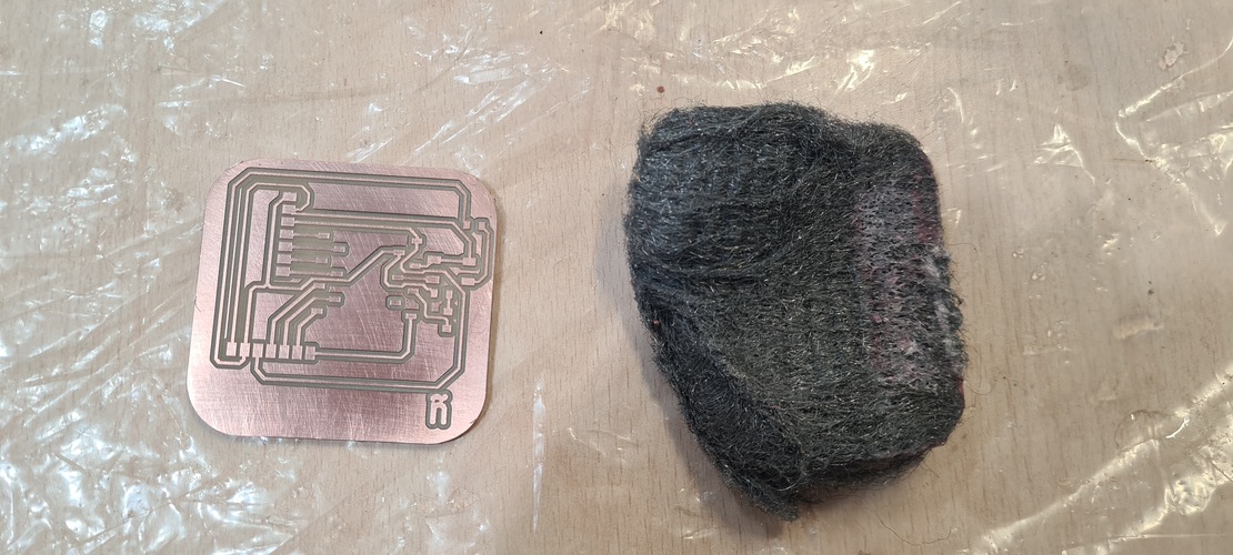
The raw material is a single-sided copper-clad FR1 board — FR1 rather than FR4 because it machines cleanly without generating fibreglass dust. Board thickness measured 1.50 mm with digital calipers.
The sacrificial board (the mártir, as Adrián calls it) sits under the copper-clad and absorbs the final millimetres of the cutout pass. Before mounting a new board, sand it lightly to remove adhesive residue from previous runs — the goal is a flat, clean surface for the tape to bond to.
operating the Roland MDX-20 step by step.
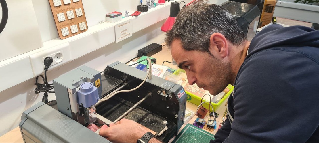
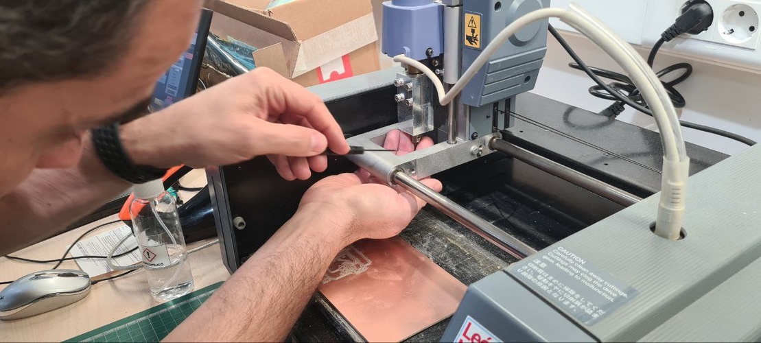
This was my first time on the MDX-20, with Adrián walking me through every step of the process. The machine needs careful Z referencing every time the tool changes.
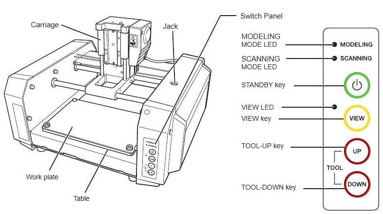
The physical controls on the MDX-20 are minimal but important to understand before running any job:
- STANDBY key — powers the machine on and off. On startup, the unit runs an initial homing sequence (audible for ~20 seconds) and then stops with the VIEW LED and MODELING MODE LED lit. Press again to power off.
- VIEW key — moves the carriage to the front of the machine for tool access and board inspection. Also used to abort a cutting operation in progress. The VIEW LED lights up when the carriage is in the view position.
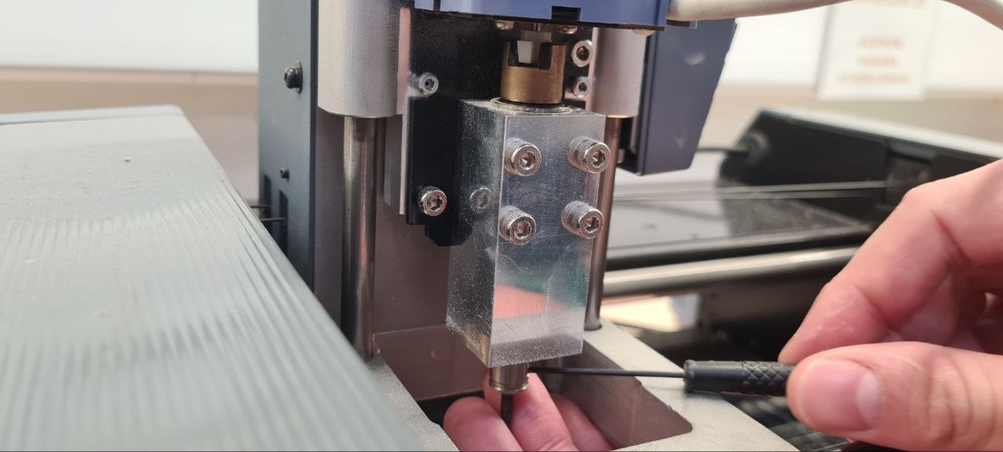
- TOOL UP / TOOL DOWN keys — raise and lower the Z axis (the spindle) manually in small increments. Used during tool changes and Z origin setting — lower the spindle until the tool tip just rests on the board surface, then lock the set screws and register Z0 in mods.
1. Power on. Press the STANDBY key. The machine runs its homing sequence and stops with the VIEW and MODELING LEDs lit.
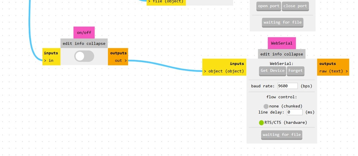
2. Connect in mods. Open mods in Chrome. In the Roland MDX / iModela node, click Get device to connect via Web Serial. A small icon in the node confirms connection. Jog the machine to verify: click XY0 and confirm the head moves to the origin position.
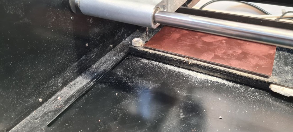
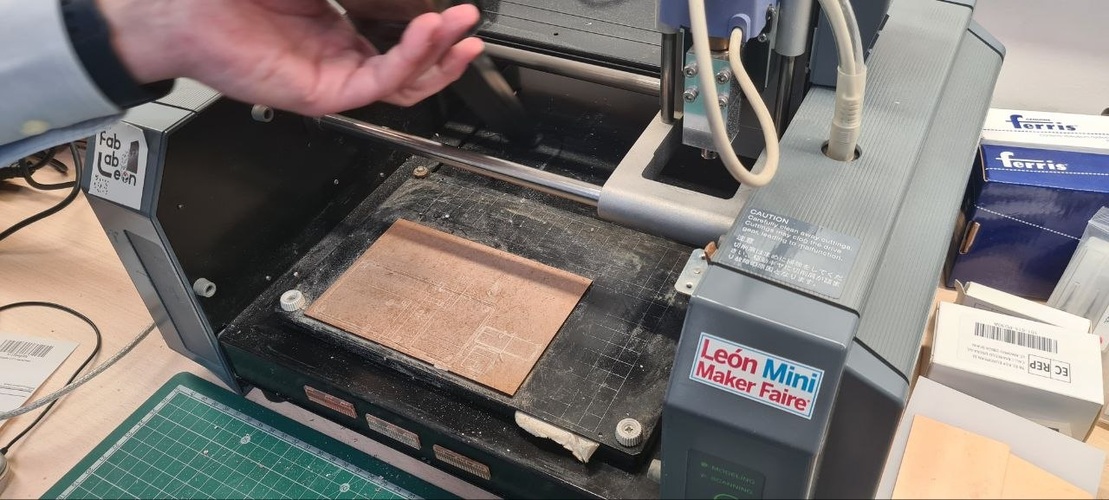
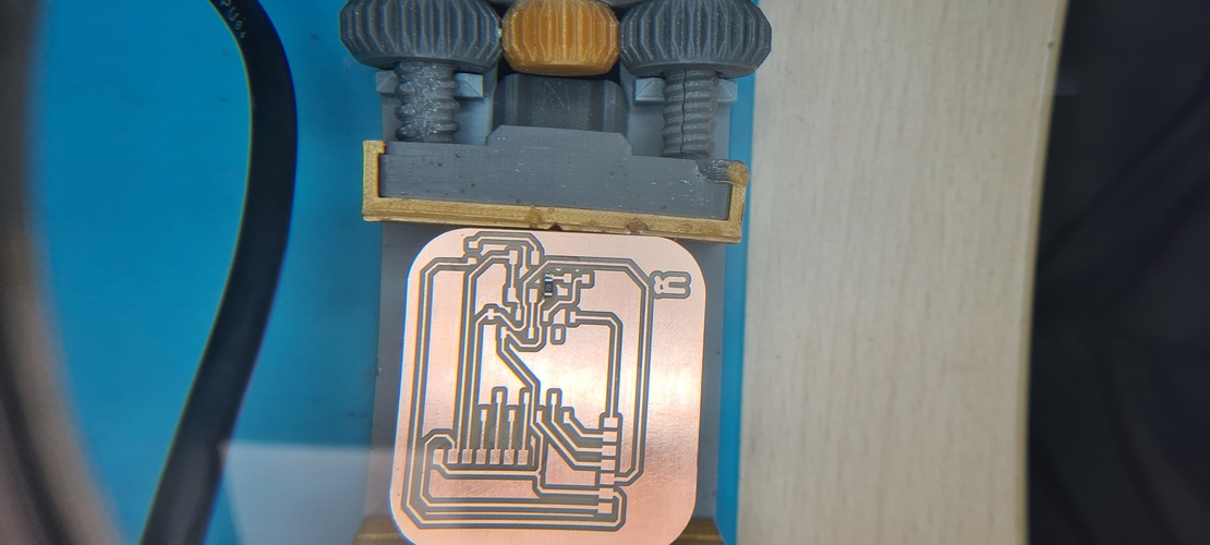
3. Mount the board. Peel the tape backing and press the FR1 blank firmly onto the sacrificial board — full surface pressure, especially at the corners. Any flex or lift will show up as uneven trace depth.
4. Set the XY origin. Use the jog controls in mods (1 mm increments) to position the spindle over the intended board corner. The origin in this session was X: 5, Y: 3 — enough margin from the edge. Click XY0 to set this as the absolute origin for the job.
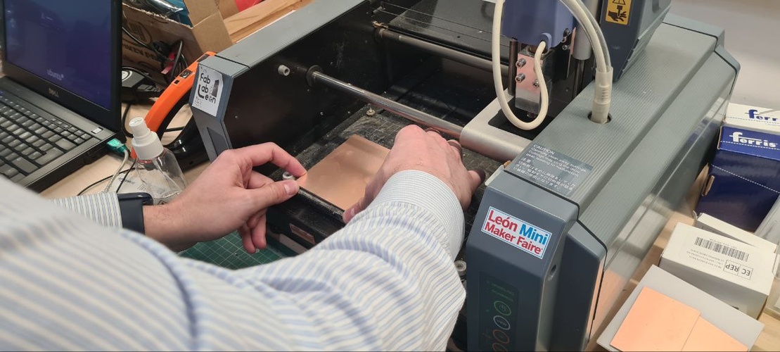
5. Set the Z origin (tool probe). This step must be repeated every time the tool changes. Loosen both set screws on the collet. Hold the spindle body steady, lower the Z axis manually until the tip of the end mill just rests on the copper surface — gravity contact, no pressure. Tighten one screw. Click Z0 in mods to register this as Z zero.
6. Load the toolpath and send. In mods, load the traces PNG, configure the parameters, click Calculate. Once the toolpath appears in the simulation, click Send file. The machine starts immediately. Close the lid before the spindle reaches cutting speed.
7. Monitor the first pass. Watch the first few seconds: the tool should touch the copper and produce a thin, clean channel. If it’s skating across without cutting (Z too high) or plunging aggressively (Z too low), stop immediately.
8. Tool change for cutout. When the traces job finishes, the spindle returns home. Do not click anything that resets the XY origin — the machine still has the correct reference from step 4. Raise Z to its maximum travel, loosen both set screws, swap the 1/64” for the 1/32” cutout mill, set Z zero again, load the cutout toolpath, and send.
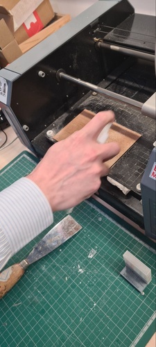
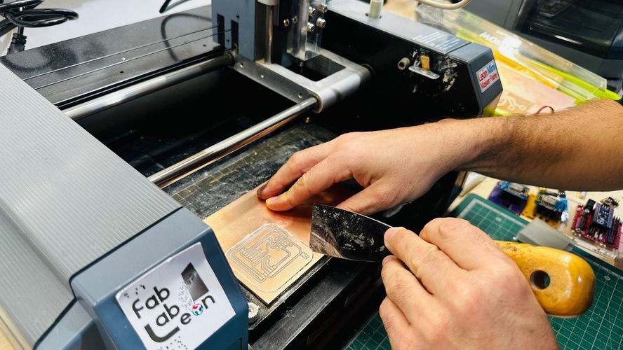
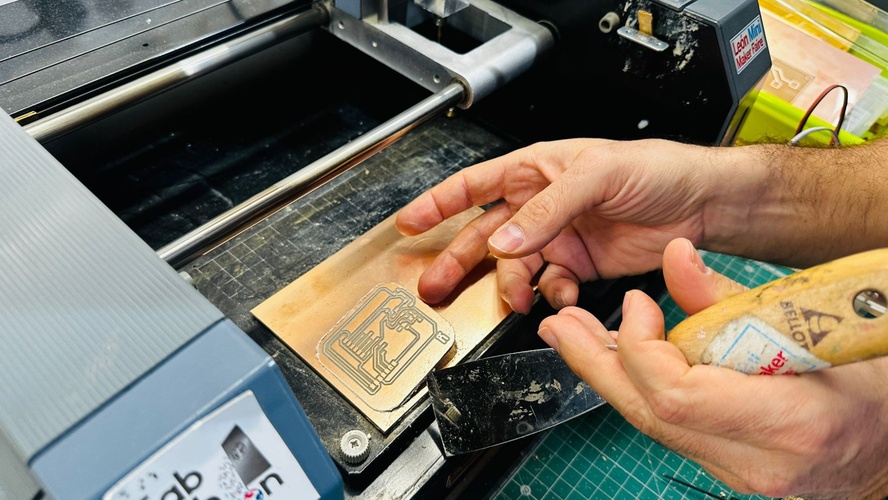
9. Extract the board. Once the cutout completes, let the spindle stop completely before opening the lid. Vacuum the copper dust — it’s conductive. Use a spatula to lift the board with gentle lateral pressure rather than peeling from above.
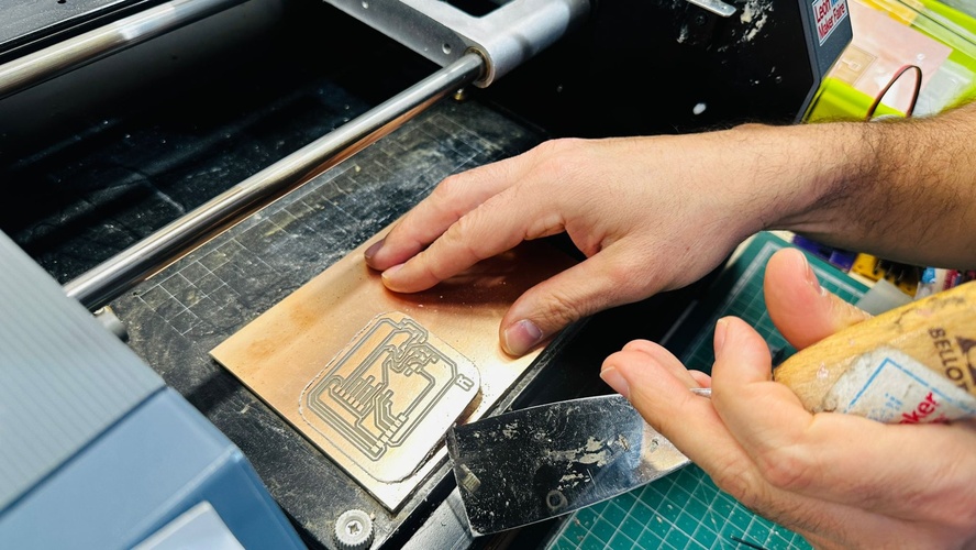
assembly & soldering.
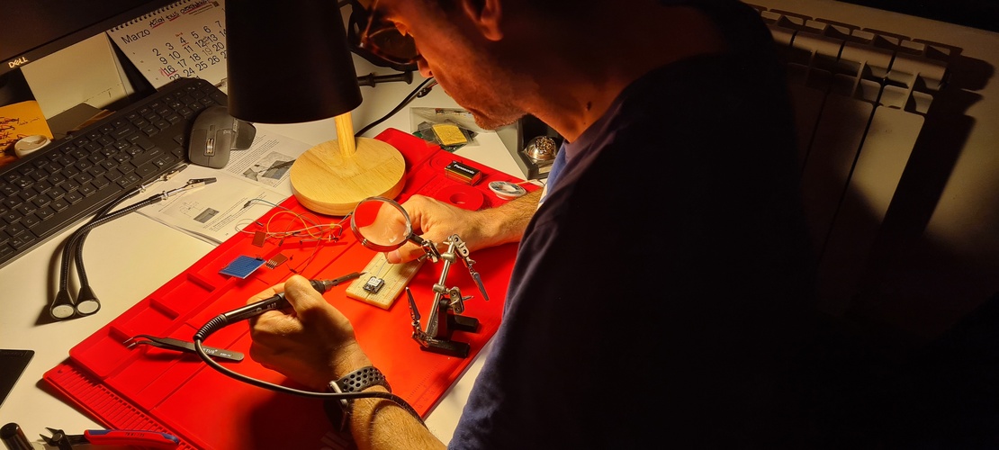
I had never soldered SMD components before this week. The scale is genuinely different from through-hole work — 1206 resistors are 3.2 × 1.6 mm, which sounds manageable until you’re trying to hold one with tweezers while positioning a soldering iron. The first session (solo practice at home) went poorly enough that I came back the next day with more questions for Adrián and Nuria. By the end of the second session the board was fully assembled, tested, and working.
good practices for SMD soldering.
These are the techniques that actually worked, distilled from two days of practice and guidance from Adrián and Nuria:

Flux first, always. Apply a small amount of flux to the pads before any heat. Flux improves wetting, prevents oxidation, and makes the solder flow where you want it instead of beading up. Without it, especially on the uncoated copper from the mill, joints come out cold and dull.
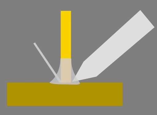
Pre-tin one pad. Before placing the component, melt a small amount of solder onto one of the two pads and let it cool. The amount matters: too much and the component will sit at an angle; too little and the bond won’t hold. Aim for a thin, slightly domed layer — barely visible.
Place, then reflow. Hold the component flat against both pads with tweezers, applying gentle downward pressure. Touch the iron to the pre-tinned pad — the solder reflows and the component locks in position. Remove the iron, wait for the joint to solidify, then release the tweezers. The component is now fixed on one side.
Solder the second pad. With the component anchored, bring a small amount of fresh solder to the second pad. The joint should be shiny and slightly concave — a volcano shape around the pad. If it’s round and balled up, there wasn’t enough heat or flux.
Control your body. Adrián’s most useful piece of advice: both hands need physical support points. Rest the wrist holding the iron on the table edge; rest the wrist holding the tweezers on the board itself or a nearby block. Free-floating hands introduce tremor that makes precise placement much harder, especially on small pads.
Inner to outer, small to large. Solder the smallest, lowest-profile components first (resistors and LED), then taller ones (switch), then the connectors (horizontal headers), and finally the XIAO socket last. Working from inside to outside keeps the board accessible at every step and avoids the iron catching on components already placed.
Verify before soldering. For polarised components — especially the LED — check orientation against the schematic before applying any heat. Once a component is soldered, desoldering it from a milled copper board is risky. The pads are thinner than on a manufactured board and can lift with repeated heat.
component inventory.
The solder used at Fab Lab León is Loctite 60/40 tin-lead, 0.38 mm diameter, with 5-core flux.

surface preparation.
Before soldering, clean the copper surface. The milling process leaves copper dust and handling oils on the surface — both prevent proper wetting.
The cleaning itself was done right after milling — see the steel-wool clean shown in the milling section, where a soap-impregnated steel wool pad removes the residual copper dust and oxidation before the board ever reaches the soldering bench.
securing the board.
A board that moves during soldering is a failed joint waiting to happen. For the practice sessions I used a 3D-printed PCB vise from the lab.
soldering process.
Resistors first. R1 (1 KΩ) and R2 (10 KΩ) went on first. Verified each value with the multimeter before placing. Pre-tinned one pad per footprint, placed, reflowed, soldered the second pad.
LED polarity. D1 required four checks before placing: schematic (cathode to GND), KiCad 3D render (orientation relative to pad markers), the LED’s physical cathode mark (shorter leg, green indicator line on the package), and the iBOM to cross-reference pad assignments. A reversed LED on a milled board is very unpleasant to fix.
Switch. SW1 is a four-pad tactile switch where the pads connect two-by-two. Orientation matters: there are two correct orientations (180° rotations of each other) and two wrong ones (90° rotations). Verified with the schematic before placing.
Horizontal pin headers (J1, J2). These are SMD-mount — the mechanical tabs solder to pads on F.Cu. Flux the pads, position the header, tack one tab to hold it, check alignment visually, then solder the remaining tabs and all signal pins.
XIAO socket (M1). Adrián’s suggestion: insert the XIAO RP2040 into the socket before soldering. This keeps the socket pins aligned to the correct spacing while you work — the XIAO’s own geometry acts as a jig. Tack two outer corner pins first, verify alignment, solder all outer pins. Remove the XIAO, then solder the inner pins (blocked by the XIAO’s body during the outer pass).
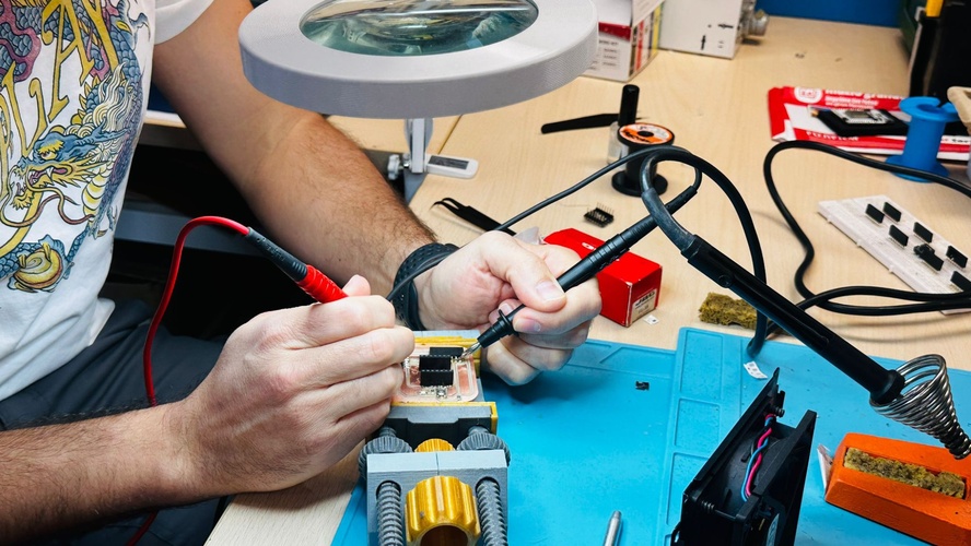
continuity testing.
After soldering, Nuria walked me through a systematic continuity check before connecting the XIAO. The logic:
- All GND points must be continuous with each other.
- All 3.3V points must be continuous with each other.
- All 5V points must be continuous with each other.
- No GND-to-3.3V or GND-to-5V continuity (short circuit).
Set the multimeter to continuity mode (beep). Touch one probe to a known GND pad and walk the other probe to every other GND-connected pad on the board. All should beep. Repeat for 3.3V and 5V rails. Then cross-check: GND probe to any 3.3V pad — no beep expected.
No shorts found. All rail continuity checks passed.
Nuria also recommended establishing a consistent pin ordering convention for the free-signal headers in future boards: always put 5V on the outermost pin, then 3.3V, then GND (or the reverse — pick one and stick with it). This board’s header layout was driven by routing constraints rather than convention, which made verification slightly harder. Worth fixing in the next design.
testing.
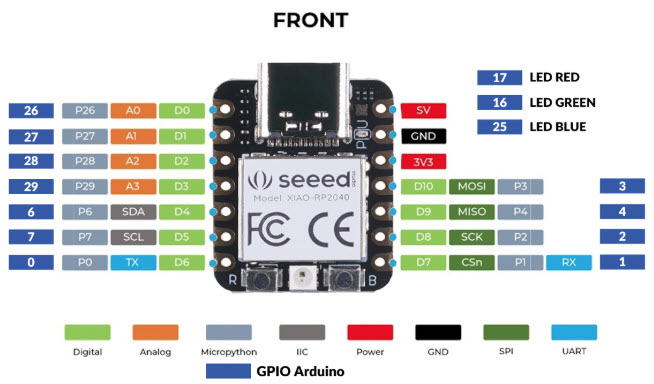
With continuity confirmed, Nuria loaded a quick blink sketch to verify the LED. There was a brief confusion about pin numbering: the LED is wired to the pin the XIAO RP2040 silk-labels as D9, but the Arduino API doesn’t use those silk numbers directly. Nuria’s first sketch, written with the silk number as the pin, didn’t work. Adrián clarified the mapping — on the XIAO RP2040, silk D9 corresponds to 4 in the Arduino API (per Seeed’s official pinout). Setting the sketch to pin 4, or equivalently the D9 macro, and re-uploading produced a blinking LED immediately.

A first, simple demo: a single button press toggles the LED on and off. This already confirms that both the button input and the LED output work on the assembled board.
To take it a step further — and to exercise the board with more than a plain on/off toggle — I wrote a small sketch that cycles the LED through three modes on each button press: off, slow blink (500 ms), and fast blink (125 ms), printing the active mode over serial at 115200 baud.
The full test sketch is below, and is also available for download in files & resources. The LED uses the D9 macro and the button D10 — the silk-aligned macros that map to GPIO4 and GPIO3, which sidesteps the pin-numbering confusion noted above. The button has an external 10 kΩ pull-down, so it reads HIGH when pressed; the sketch declares it INPUT, not INPUT_PULLUP. The blink is non-blocking (millis()-based) and the button is debounced with rising-edge detection so each physical press advances the mode exactly once.
tab: week08-blink-modes.ino | week08-blink-modes.ino
// Week 08 — board functionality test (Week 06 XIAO RP2040 breakout).
// One button cycles the LED through three modes: OFF -> SLOW -> FAST -> OFF...
// Non-blocking (millis-based). Button is active-HIGH (external 10k pull-down).
//
// Pin mapping note (XIAO RP2040, Earle Philhower core):
//   silk D9  = GPIO4  -> the LED
//   silk D10 = GPIO3  -> the button
// Using the D9/D10 macros instead of raw integers keeps the code aligned with
// the board silk and removes the silk-vs-GPIO confusion entirely.

const int LED_PIN    = D9;   // silk D9  (GPIO4)
const int BUTTON_PIN = D10;  // silk D10 (GPIO3), external pull-down -> pressed = HIGH

const unsigned long DEBOUNCE_MS      = 30;   // stable window before a reading counts
const unsigned long SLOW_INTERVAL_MS = 500;  // half-period of the slow blink
const unsigned long FAST_INTERVAL_MS = 125;  // half-period of the fast blink

enum Mode { MODE_OFF, MODE_SLOW, MODE_FAST };
Mode currentMode = MODE_OFF;

bool ledState = false;                 // current LED output level
unsigned long lastBlinkTime    = 0;    // last LED toggle timestamp
unsigned long lastDebounceTime = 0;    // last raw-reading change timestamp
int lastButtonReading = LOW;           // previous raw reading (for change detection)
int buttonState       = LOW;           // debounced, stable button state

void setup() {
  pinMode(LED_PIN, OUTPUT);
  pinMode(BUTTON_PIN, INPUT);          // external pull-down: do NOT use INPUT_PULLUP
  digitalWrite(LED_PIN, LOW);
  Serial.begin(115200);
}

void loop() {
  handleButton();   // detect a debounced press and advance the mode
  updateLed();       // drive the LED according to the current mode
}

// --- button: debounce + rising-edge detection ---
void handleButton() {
  int reading = digitalRead(BUTTON_PIN);

  if (reading != lastButtonReading) {
    lastDebounceTime = millis();       // input moved: restart the debounce timer
  }

  if (millis() - lastDebounceTime > DEBOUNCE_MS) {
    // the reading has been stable long enough to be trusted
    if (reading != buttonState) {
      buttonState = reading;
      if (buttonState == HIGH) {       // LOW -> HIGH transition = a real press
        advanceMode();
      }
    }
  }

  lastButtonReading = reading;
}

void advanceMode() {
  switch (currentMode) {
    case MODE_OFF:  currentMode = MODE_SLOW; break;
    case MODE_SLOW: currentMode = MODE_FAST; break;
    case MODE_FAST: currentMode = MODE_OFF;  break;
  }

  // start the new mode from a clean phase
  lastBlinkTime = millis();
  ledState = false;
  digitalWrite(LED_PIN, LOW);

  Serial.print("Mode -> ");
  Serial.println(currentMode == MODE_OFF  ? "OFF"
               : currentMode == MODE_SLOW ? "SLOW"
                                          : "FAST");
}

// --- LED: non-blocking blink according to the current mode ---
void updateLed() {
  if (currentMode == MODE_OFF) {
    if (ledState) {                    // make sure it ends up off
      ledState = false;
      digitalWrite(LED_PIN, LOW);
    }
    return;
  }

  unsigned long interval =
      (currentMode == MODE_SLOW) ? SLOW_INTERVAL_MS : FAST_INTERVAL_MS;

  if (millis() - lastBlinkTime >= interval) {
    lastBlinkTime = millis();
    ledState = !ledState;
    digitalWrite(LED_PIN, ledState ? HIGH : LOW);
  }
}
tab: end
Running the three-mode sketch: each button press advances the LED through off → slow → fast → off, captured alongside the Serial Monitor (115200 baud), which prints each mode change in sync.
conclusions.
The design side of this week was more involved than expected. Adding two expansion headers forced several routing iterations and made me appreciate how sensitive single-layer PCB routing is to component placement decisions. Moving a footprint after routing in KiCad means manually rerouting every affected trace — there’s no intelligent track-following on repositioning. Something to plan for upfront: finalise placement before touching the router.
The pull-down correction on the button was a good reminder that circuit correctness matters even on simple boards. A pull-up versus pull-down isn’t just a naming detail — it inverts the logic level the firmware reads and can produce confusing behaviour that’s easy to miss if you’re not measuring it.
mods is a powerful tool once you understand the node graph model. The workflow (PNG in → toolpath out → machine file) is logical, and the simulation view is genuinely useful for catching obvious problems before cutting. Use Chrome or Chromium — the Web Serial API support is consistent and verified.
The SMD soldering was the biggest learning curve. SMD components at 1206 scale are manageable once you have a workflow, but that workflow took two sessions and a lot of questions to establish. The key insight — pre-tin one pad, place, reflow, then solder the second — is standard practice but feels unintuitive until you’ve done it a few times. The XIAO-as-jig technique for the socket alignment is one I’ll use on every future board.
The pin numbering discrepancy between the XIAO’s silk labels and Arduino’s API numbering is worth documenting: D9 on the board → 4 in Arduino. Seeed’s XIAO RP2040 pinout reference has the full mapping.
files & resources.
- Interactive BOM
- Test sketch (three-mode LED/button blink, Arduino): week08-blink-modes.ino
- KiCad project (.zip)
- Gerber files (.zip)
- Roland Modela Mdx-20 User Manual
- mods CE
- InteractiveHtmlBom plugin
- XIAO RP2040 pinout — Seeed Wiki
- Week 08 class notes — Fab Academy 2026
- Fab Lab León 2026 Group Page