Input devices
weekly schedule.
| Time block | Wed | Thu | Fri | Sat | Sun | Mon | Tue | Wed |
|---|---|---|---|---|---|---|---|---|
| Global class | 3 h | |||||||
| Local class | 1,5 h | 1,5 h | ||||||
| Research | 1 h | 2 h | ||||||
| Design | 2 h | 2 h | 1 h | |||||
| Fabrication | 2 h | |||||||
| Documentation | 2 h | 3 h | 1 h | |||||
| Review |
overview.
This week covers input devices — designing and building a board that reads a physical sensor and produces usable data. The assignment requires going through the full cycle: design in KiCad, generate toolpaths in Mods CE, mill on the Roland MDX-20, solder, and validate with code.
The sensor choice evolved during the week. My initial plan was to design a custom PCB around the TLE493D-A2B6 — a 3D magnetometer in a TSSOP-6 package, hand-solderable with a fine-tip iron, which made it attractive as a way to avoid reflow soldering. I also assumed its footprint would be more manageable than the VL53L1X bare chip. I started down that path in KiCad, but Nuria (Fab Lab León instructor) pointed out that using a breakout module was a valid option for the assignment. That shifted the focus: the VL53LXX time-of-flight breakout available at the lab became the main sensor for this week, while the TLE493D board design continues as a parallel spiral.
learning objectives.
- Design a sensor breakout board in KiCad 9 for an I2C device.
- Understand pull-up requirements for I2C buses and decoupling for sensitive analog-adjacent circuits.
- Mill and solder a board with TSSOP-6 SMD components.
- Read I2C data in Arduino and correlate raw sensor values with physical position.
- Capture I2C frames with the logic analyzer for the group assignment.
assignments.
- Individual assignment: measure something — design and build a board to interact with an input device, then read it.
- Group assignment: probe an input device’s analog levels and digital signals.
research.
I2C — what it is and how it works.
Before designing the board I needed to understand I2C properly, because both sensors I evaluated use it exclusively, and I had only used it through libraries without thinking much about what was actually happening on the wire.
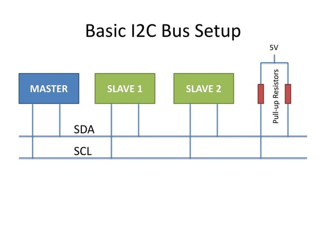
I2C (Inter-Integrated Circuit) is a serial communication protocol designed to connect multiple devices using just two wires. That is the main appeal: instead of dedicating one pin per device, you share a single bus and every device gets an address. The XIAO RP2040 acts as the master — it initiates all communication — and the sensor acts as a slave, responding only when addressed.
The two lines are SDA (Serial Data) and SCL (Serial Clock). SCL carries a clock signal generated by the master; SDA carries data in both directions, one bit per clock pulse. Both lines are shared by all devices on the bus.
What makes I2C unusual compared to simpler protocols is that both lines are open-drain. No device ever drives a line HIGH — they can only pull it LOW by connecting the line to GND through an internal transistor. When nothing is pulling the line LOW, it needs something external to bring it back HIGH. That is the job of the pull-up resistors: they connect SDA and SCL to VCC so the lines default to HIGH when the bus is idle.
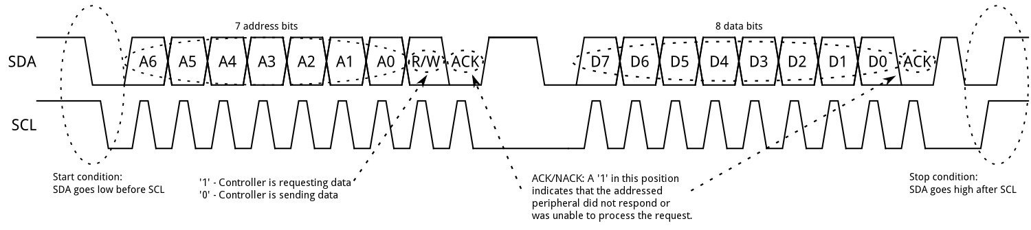
A typical transaction looks like this: the master sends a START condition (SDA goes LOW while SCL is still HIGH — a specific pattern that all devices on the bus recognise as “pay attention”). Then it sends a 7-bit address identifying which slave it wants to talk to, followed by a read/write bit. The addressed slave responds with an ACK (it pulls SDA LOW for one clock pulse to confirm it is there). Then data bytes flow — each one acknowledged — until the master sends a STOP condition (SDA goes HIGH while SCL is HIGH) to release the bus.
The logic analyzer captures all of this. Watching a real I2C transaction is probably the clearest way to understand the protocol — the group assignment covers that part.
VL53LXX time-of-flight sensor — why it is relevant to the final project.
The VL53LXX is a time-of-flight distance sensor. It emits infrared pulses at 940 nm and measures the time they take to return after reflecting off a surface. From that, it calculates absolute distance in millimetres, with a useful range of roughly 4 cm to 4 m — no mechanical contact required.
For the final project (a height-adjustable desk with four motorised legs), knowing each leg’s absolute position at all times is critical. If a motor loses steps due to an obstruction or a sudden load change, a position sensor catches the discrepancy — the leg is at a different height than the firmware thinks. In a four-leg system, that kind of desynchronisation causes the desk to tilt. A VL53LXX mounted at the base of each leg, pointing upward along the travel axis, would provide continuous closed-loop position feedback independent of step counting.
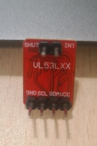
The original plan was to design a custom PCB around the TLE493D-A2B6 magnetometer. After starting the KiCad design, Nuria suggested using a breakout module instead — a valid approach for the assignment that also sidesteps the reflow constraint of the bare VL53L1X chip, whose LCC package has pads underneath that cannot be soldered reliably with a hand iron. The VL53LXX breakout available at the lab already has the sensor soldered, the pull-up resistors and decoupling capacitor integrated, and four accessible header pins (GND, SCL, SDA, VCC). From that point the breakout became the primary sensor for this week’s validation work, while the TLE493D PCB design continues as a parallel spiral.
group assignment.
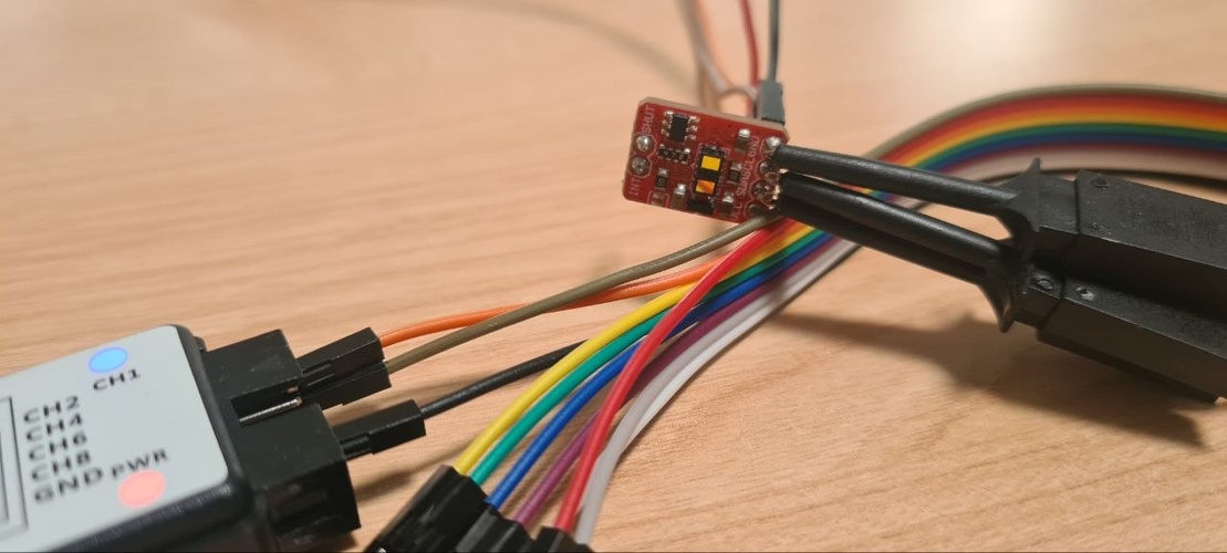
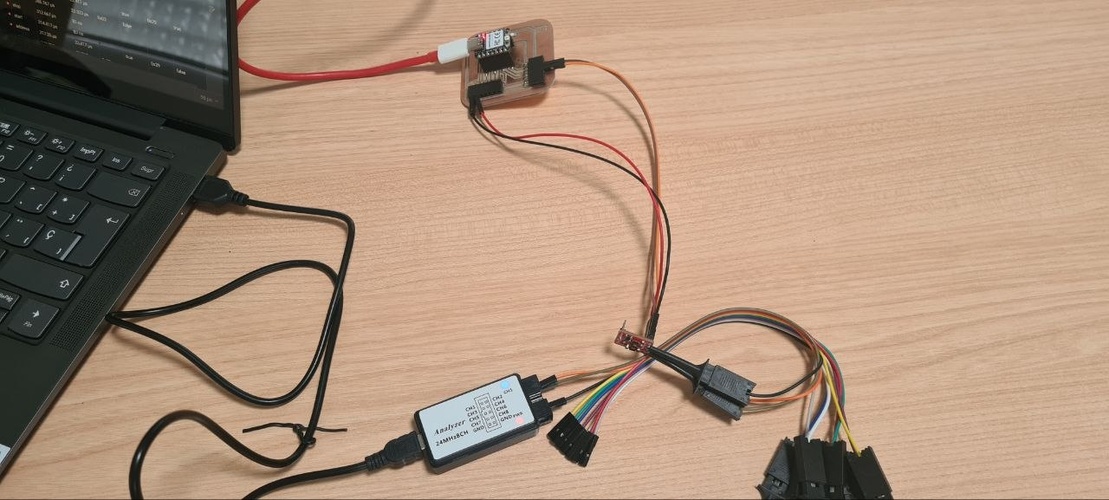
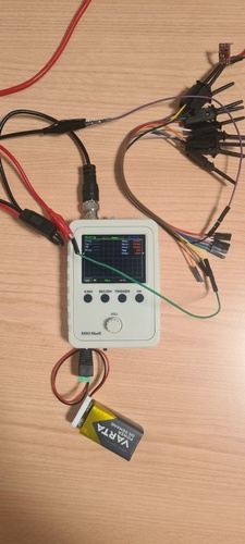
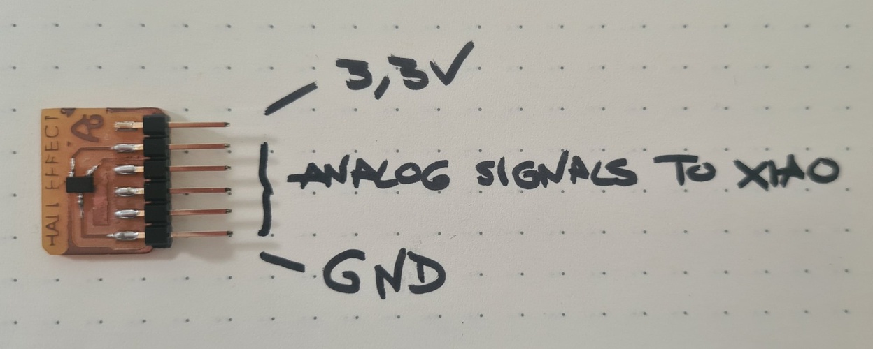
The group assignment for this week required probing an input device’s analog levels and digital signals. Two complementary instruments were used: a logic analyzer to capture and decode the digital I2C frames, and a DSO Shell oscilloscope to measure the analog voltage levels on the same bus lines. The VL53LXX time-of-flight sensor provided the digital signal source; the Hall effect sensor from the lab (Adrián Torres’ board) provided a purely analog signal for contrast.
capturing I2C frames with the logic analyzer.
The logic analyzer used is a 24 MHz 8-channel USB device running Logic 2 v2.4.43 by Saleae. The connection is in parallel with the existing circuit — the analyzer probes the same SDA and SCL lines without interrupting them:
| Logic analyzer | Connection point |
|---|---|
| CH0 (D0) | SDA |
| CH1 (D1) | SCL |
| GND | GND |
The I2C analyzer was configured in Logic 2 with SDA assigned to channel D0 and SCL to D1. The sampling rate was set to 12 MS/s — 30 samples per clock cycle at 400 kHz, well above the minimum needed to resolve the waveform.
A mistake worth documenting — the scale error.
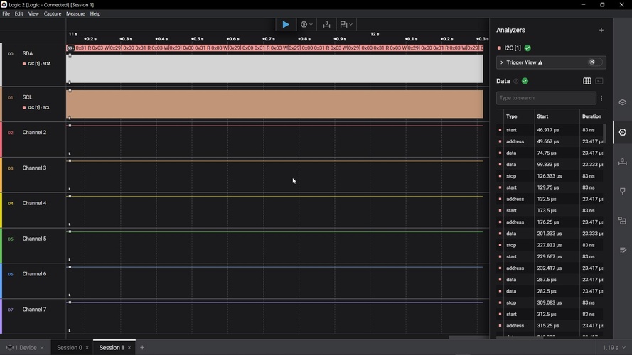
The time scale was set to display about one full second of data, compressing thousands of clock pulses into a few pixels. The fix was to zoom in with Ctrl+scroll until reaching the microsecond range.
The correct capture.
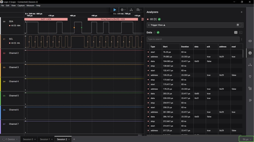
With the time scale corrected to 56 µs per division, the bus activity is fully readable. The decoder overlay shows two consecutive transactions: the XIAO writes register address 0x31 to the sensor, then addresses it again for a read at address 0x29. All ACK bits show true — the sensor responds correctly to every byte. No NACK events appear.
analog levels with the oscilloscope.
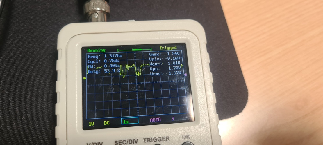
The oscilloscope used is a DSO Shell — a pocket-sized kit instrument with a bandwidth of approximately 200 kHz. At 400 kHz I2C this is below the Nyquist limit for the clock signal, so waveform edges appear rounded and frequency measurements are approximate. This is a known limitation of the instrument and is noted where relevant.
🤖 Claude (Anthropic) on the DSO Shell bandwidth limitation prompt:
I’m measuring I2C signals at 400 kHz with the DSO Shell oscilloscope from Fab Lab León, which has a bandwidth of approximately 200 kHz. The waveform edges look rounded and the frequency it measures is around 154 kHz instead of 400 kHz. Is this expected? What does it mean technically?
Yes, this is completely expected. The DSO Shell’s ~200 kHz bandwidth means it cannot faithfully reproduce signals above that frequency. At 400 kHz I2C, the clock frequency is already twice the instrument’s bandwidth limit — the Nyquist theorem requires a bandwidth of at least twice the signal frequency for accurate reproduction. The effect is that fast transitions get low-pass filtered: sharp edges become rounded curves, and the measured frequency appears lower than the actual one. The voltage levels (HIGH and LOW) are still readable because they are DC values, not frequency-dependent. The apparent negative Vmin is an overshoot artefact caused by ringing on fast transitions. For this application — documenting that the bus is electrically healthy and voltage levels are correct — the DSO Shell is adequate. For precise timing measurements you would need at least 800 kHz–2 MHz bandwidth.
The probe was connected to SDA (red) and GND (black, referenced to the XIAO GND pin). Scale: 1 V/div, 10 µs/div, trigger AUTO.
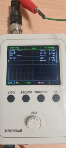
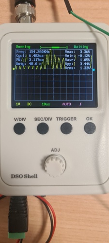
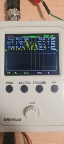
The contrast between SDA and SCL is clear: SDA shows irregular bursts encoding data bits, while SCL shows a regular continuous clock during the transaction window. Both lines share the same voltage levels — HIGH at ~3.3 V maintained by the pull-up resistors, LOW at ~0 V when pulled down by the driving device.
The DSO Shell displays several parameters alongside the waveform. Here is what each one means in this context:
| Parameter | Value (typical) | Meaning |
|---|---|---|
| Freq | ~78–154 kHz | Apparent frequency as measured by the DSO Shell. Underestimates the actual 400 kHz I2C clock due to the instrument’s ~200 kHz bandwidth limit. |
| Cycl | ~0.012 ms | Period of one apparent cycle (1 / measured frequency). |
| PW | ~0.004 ms | Pulse width — duration of the HIGH state within one measured cycle. |
| Duty | ~35–48 % | Duty cycle — percentage of time the signal spends HIGH. A symmetric 400 kHz clock would show ~50%; the deviation is a bandwidth artefact. |
| Vmax | ~3.4 V | Maximum voltage — the HIGH level maintained by the 4.7 kΩ pull-up resistor to 3.3 V. |
| Vmin | ~−0.4 V | Minimum voltage. The apparent negative value is an overshoot artefact caused by the DSO Shell’s limited bandwidth on fast falling edges — the actual LOW is ~0 V. |
| Vavr | ~0.7 V | Average voltage over the capture window. Low because the line spends most of the time LOW during an active transaction. |
| Vpp | ~3.8 V | Peak-to-peak voltage (Vmax − Vmin) — the full swing of the signal between HIGH and LOW. |
| Vrms | ~1.3 V | RMS voltage — the equivalent DC value that would deliver the same power. Not directly relevant for digital signals but confirms the signal is active. |
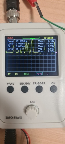
hall effect sensor — analog signal with the oscilloscope.
The Hall effect sensor on the lab board (Adrián Torres’ board) is an Allegro A1324 — a linear, ratiometric Hall sensor that outputs an analog voltage proportional to the magnetic flux density (field strength) along its sensitive axis. At zero field the output sits at about half the supply voltage (the quiescent point) and swings above or below as a magnet approaches. So the magnitude being measured is field strength, not distance. Unlike the VL53LXX, there are no I2C frames to capture — the signal is a slowly varying DC voltage, making it a useful complement to the digital captures above for the group assignment.
The sketch used is the one provided by Adrián Torres (Fab Lab León, 2023). It reads the analog voltage on pin A0, maps the raw ADC value to a 0–1024 range, and prints it over serial at 50 ms intervals.
tab: Hall effect sensor | hall-effect.ino
//Fab Academy 2023 - Fab Lab León
//Hall effect
//Fab-Xiao

int sensorPin = A0;   // analog input pin RP2040 pin 26 or ESP32-C3 pin A0
int sensorValue = 0;  // variable to store the value coming from the sensor

void setup() {
  Serial.begin(115200); // initialize serial communications
}

void loop() {
  sensorValue = analogRead(sensorPin); // read the value from the sensor
  sensorValue = map(sensorValue, 200, 800, 1024, 0);
  Serial.println(sensorValue); // print value to Serial Monitor
  delay(50); // short delay so we can actually see the numbers
}
tab: end
The map() call remaps the raw ADC range (200–800) to 0–1024. Values below 200 or above 800 are clamped. The output is intentionally inverted — 0 maps to 1024 and 800 maps to 0 — so that the displayed value increases as the magnet moves away and decreases as it approaches. The number printed is not a physical unit: it is the analog output (proportional to field strength) read by the ADC and rescaled. It tracks how strong the field at the sensor is, not a distance.
The oscilloscope probe was connected to pin A0 (red) and GND (black). Scale: 1 V/div, the time scale varied between 10 µs and 1 s depending on what was being captured.
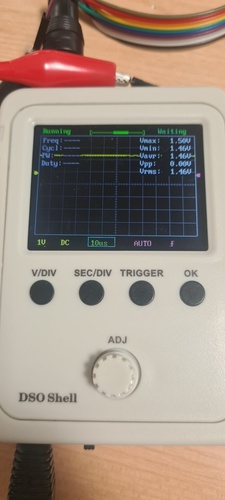
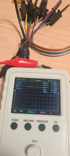
The Hall effect output contrasts clearly with the I2C signals captured on the VL53LXX: where those were digital transitions between defined HIGH and LOW levels at fixed timing, this is a continuous analog voltage that drifts slowly in response to a physical stimulus. Both capture modes together satisfy the group assignment requirement to probe both analog levels and digital signals.
design.
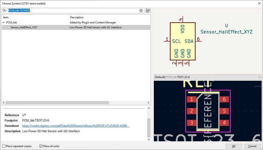
spiral 0 — TLE493D magnetometer board.
The board is intentionally minimal: the TLE493D sensor, two pull-up resistors, one decoupling capacitor, and a 4-pin connector (VCC, GND, SDA, SCL) to connect to the XIAO RP2040 board from Week 08.
A mistake worth noting. During Neil’s class, the magnetic field sensor section covered two categories: simple analog Hall effect sensors (hello.mag.45, hello.mag.t412) that output a single voltage proportional to field strength, and 3D vector magnetometers like the TLE493D that measure the field in X, Y and Z simultaneously. I picked the TLE493D by mistake — and the KiCad footprint name
Sensor_HallEffect_XYZreinforced the confusion, since it contains “HallEffect” and looked right. For the assignment itself, a simple analog Hall (like Adrián’s board) would have been the more appropriate and far simpler component to work with. But neither type suits the final project: as the detection-range note below explains, both measure magnetic field strength at close range, not absolute position over a 530 mm leg — which is why the magnetic route was ultimately dropped in favour of the time-of-flight sensor.
How the TLE493D works, and its detection range. Following Nuria’s review, I checked the datasheet and product page and Infineon’s design notes. The TLE493D-A2B6 is a 3D Hall magnetometer: it measures the magnetic flux density along three axes (Bx, By, Bz; ±160 mT full scale) and infers position from how a nearby magnet’s field changes — it does not measure distance. Its usable range is therefore tiny. Infineon’s own joystick design guide for this exact sensor uses a 1 mm air gap, and because a small magnet’s field falls off with the cube of distance (B ∝ 1/d³), a workable signal (~10 mT) only survives over a few millimetres — up to perhaps ~1–2 cm with a strong magnet, which matches the ~2 cm ceiling Nuria pointed out.
For a telescopic leg with 530 mm of travel this is a non-starter: keeping a usable field at half a metre would need a magnet thousands of times stronger, and the 1/d³ falloff makes absolute position over that range impossible to resolve. This is the quantitative backing for the conclusion above — the TLE493D is a millimetre-scale position sensor for knobs, joysticks and gear sticks, correctly ruled out in favour of the time-of-flight sensor, which measures absolute distance across the full range.
Component list:
| Reference | Component | Value | Package |
|---|---|---|---|
| U1 | TLE493D-A2B6 | — | TSSOP-6 |
| R1 | Pull-up resistor (SDA) | 4.7 kΩ | 1206 |
| R2 | Pull-up resistor (SCL) | 4.7 kΩ | 1206 |
| C1 | Decoupling capacitor (VCC) | 100 nF | 1206 |
| J1 | I2C connector | 4-pin header | — |
The TLE493D-A2B6 symbol is available in the PCM_fab library under the name Sensor_HallEffect_XYZ — a low power 3D Hall sensor with I2C interface in a TSOT-23-6 footprint.
Why two resistors, and why pull-up?
I2C is an open-drain bus. Neither the master (the XIAO) nor the slave (the TLE493D) drives the SDA or SCL lines HIGH actively — they can only pull them LOW by connecting the line to GND through an internal transistor. When neither device is pulling the line LOW, it would float to an undefined voltage and the bus would be unusable.
Pull-up resistors solve this: they connect SDA and SCL to VCC (3.3 V in this design) through a resistor. When no device is pulling the line LOW, the resistors hold both lines at a defined HIGH level. When a device pulls the line LOW, current flows through the resistor to GND. The bus works correctly in both states.
There is one pull-up per line because SDA and SCL are independent signals with different timing. Sharing a single resistor between them is not possible — they would short together.
Why 4.7 kΩ?
The I2C specification defines a maximum rise time for the bus lines — 1000 ns in standard mode (100 kHz), 300 ns in fast mode (400 kHz). The rise time is determined by the RC constant formed by the pull-up resistor and the total bus capacitance (wire, PCB traces, input capacitances of all connected devices). A smaller resistor charges the bus capacitance faster (shorter rise time) but draws more current. A larger resistor draws less current but slows the rise time.
4.7 kΩ is a well-established default for short I2C buses at 100–400 kHz with a 3.3 V supply. At 3.3 V and 4.7 kΩ, each resistor draws about 0.7 mA when the line is pulled HIGH — well within the XIAO RP2040’s supply capability. For the trace lengths involved in this board (a few centimetres), the bus capacitance is low and the 4.7 kΩ value gives comfortable margins.
The Fab Lab inventory has 4.99 kΩ resistors (1206, RC1206FR-074K99L) as the closest available value. 4.99 kΩ is electrically equivalent to 4.7 kΩ for this application — the difference is negligible.
Why a decoupling capacitor, and why 100 nF?
The TLE493D measures magnetic field strength in three axes using Hall effect elements inside the chip. These elements are sensitive to very small voltage fluctuations on the supply pin — any noise on VCC directly corrupts the measurement. When digital logic switches inside the chip (or anywhere else on the board), it draws short current pulses from the supply. Without a local capacitor, these pulses propagate as voltage spikes along the supply trace.
A decoupling capacitor placed as close as possible to the VCC pin of the TLE493D acts as a local energy reservoir: it absorbs those current spikes before they cause a voltage drop, keeping VCC stable for the analog circuitry inside the sensor.
100 nF (0.1 µF) is the standard value for high-frequency decoupling. The impedance of a capacitor decreases with frequency — a 100 nF ceramic capacitor has low impedance in the MHz range, which is exactly where switching transients from digital logic fall. Below that range (slow supply variations), the PCB traces and the power supply itself handle regulation. Above it, parasitic inductance in the capacitor’s own leads becomes dominant. 100 nF sits in the right window for this application.
The capacitor is placed on the same layer as the TLE493D, as close to its VCC pin as the layout allows, with the return path to GND kept short.
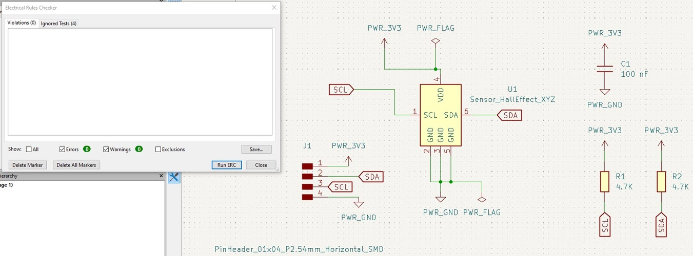
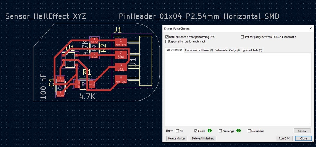
ERC and DRC.
Both checks pass with zero violations and zero warnings.
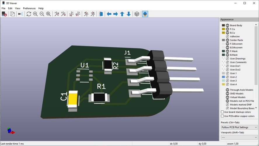
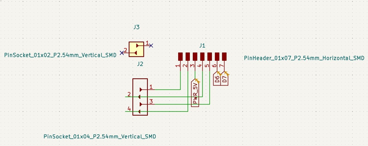
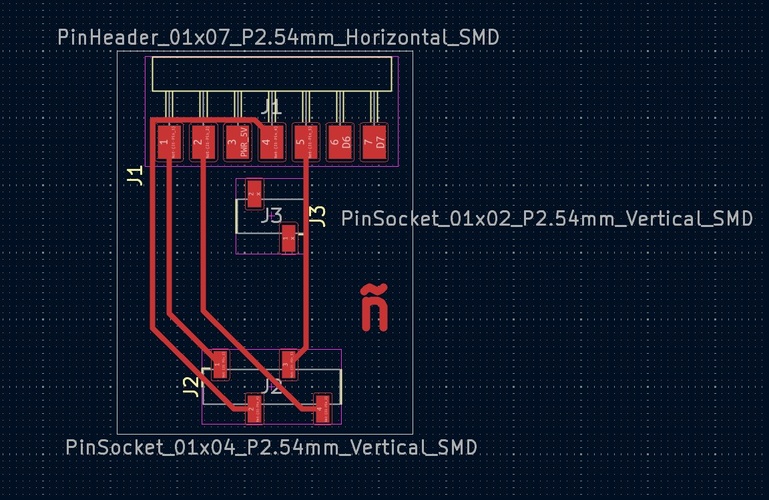
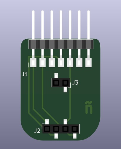
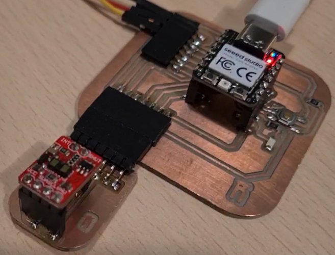
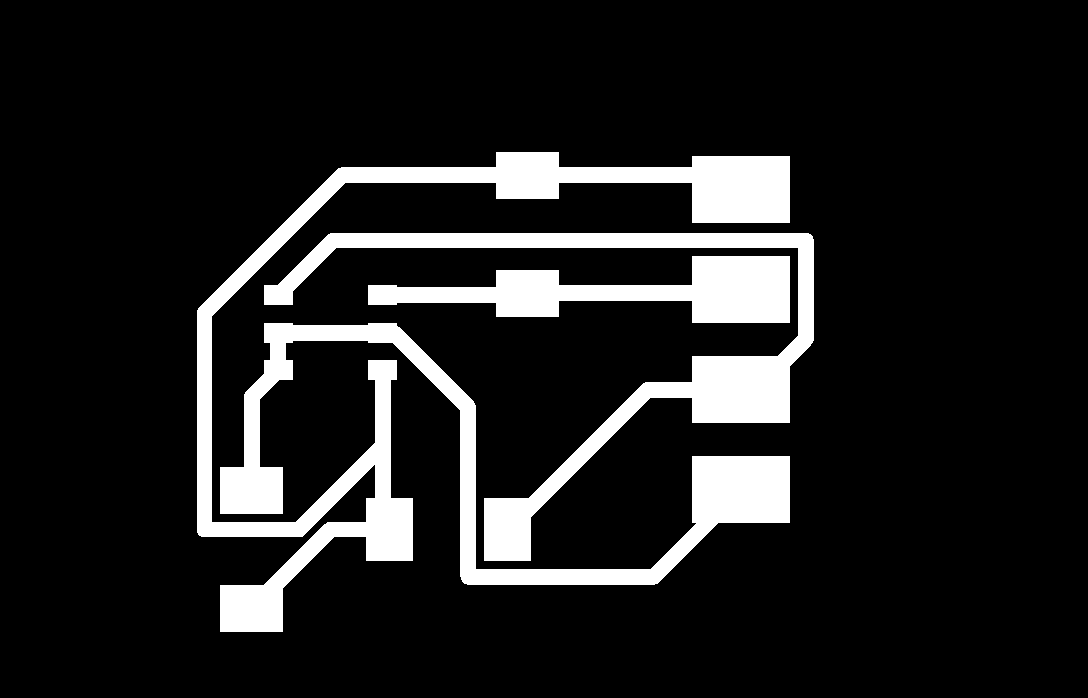
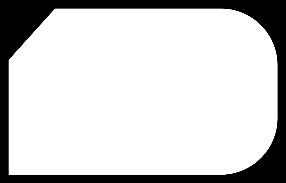
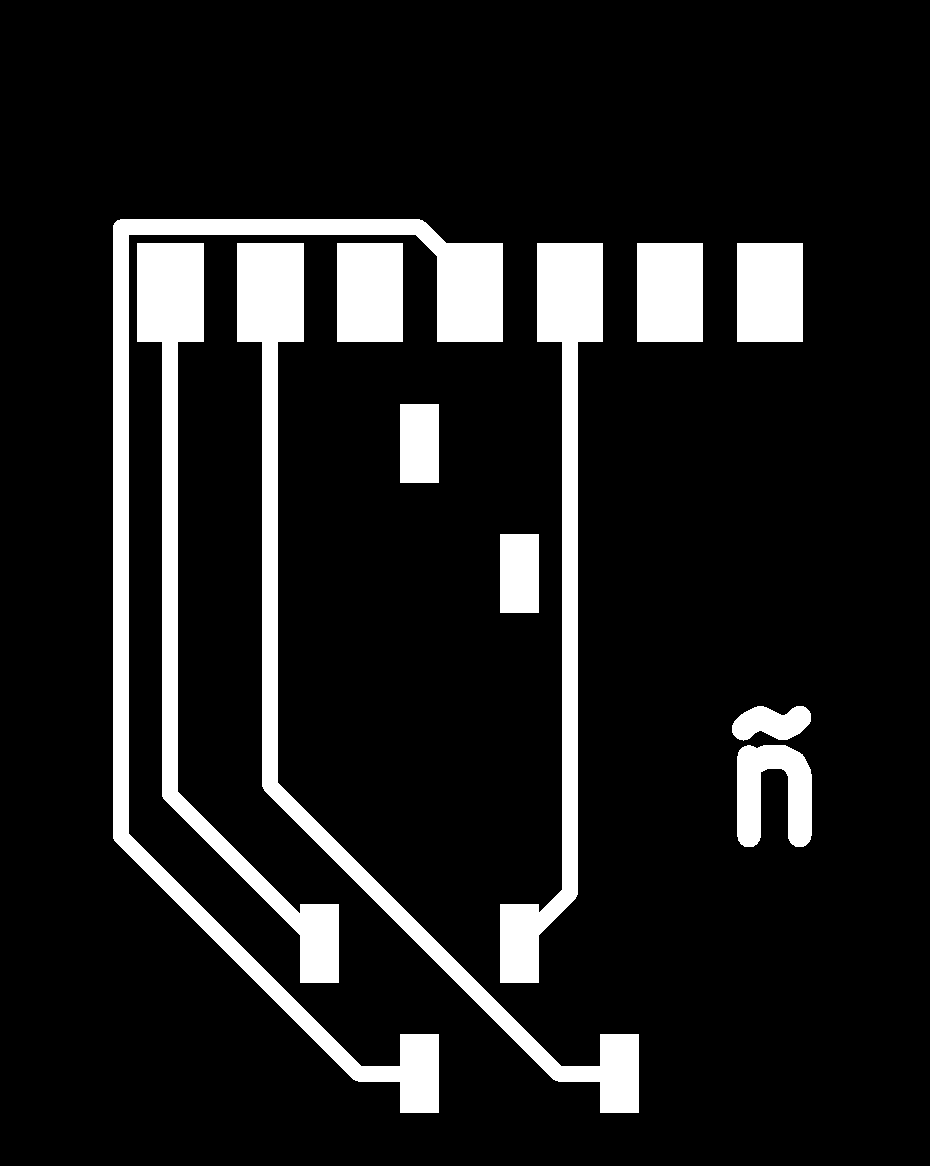
spiral 1 — VL53LXX ToF adapter board.
Rather than wiring the breakout directly to the XIAO with loose jumpers, I designed a small adapter PCB that gives the module a proper mechanical home. The board has two pin sockets that accept the VL53LXX breakout (J2: 4-pin for GND/SCL/SDA/VCC, J3: 2-pin for SHUT/INT as mechanical support only) and a 7-pin horizontal header (J1) that plugs directly into the XIAO board from Week 08.
No additional passive components are needed — the breakout already carries the pull-up resistors and decoupling capacitor.
Before placing the sockets in KiCad, the physical distance between the two pin groups on the breakout had to be measured to ensure the footprints would align with the actual component.
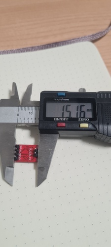
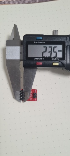
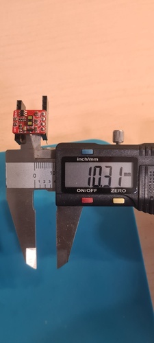
The most reliable measurement came from inserting both sockets into the breakout physically and measuring the resulting gap with calipers — 10.31 mm centre to centre. This eliminates any ambiguity about whether the theoretical 2.54 mm pin pitch applies uniformly across the full board width.
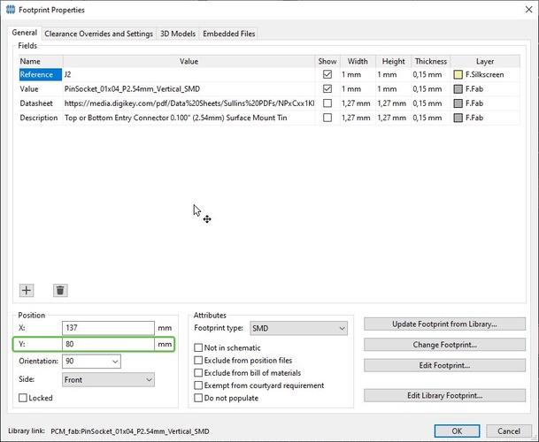
To place the footprints at an exact distance in KiCad, the fastest method is to open the Footprint Properties of the second component (double-click on it in the PCB editor) and set the X or Y coordinate directly. With J2 placed at Y = 69.69 mm and the required separation of 10.31 mm, J3 goes at Y = 80 mm. No manual dragging or grid snapping required — the value is entered directly in the Position field.
fabrication.
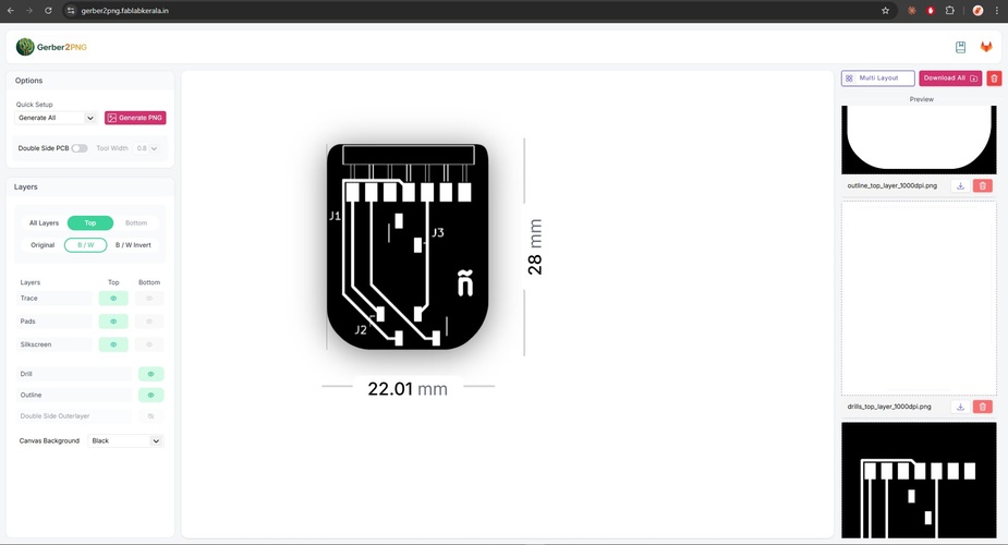
With the PCB design validated, Gerber files were exported from KiCad via Fabrication Outputs → Gerbers including the drill files. Those were uploaded to gerber2png.fablabkerala.in, which generates the PNG files needed to load into Mods CE.
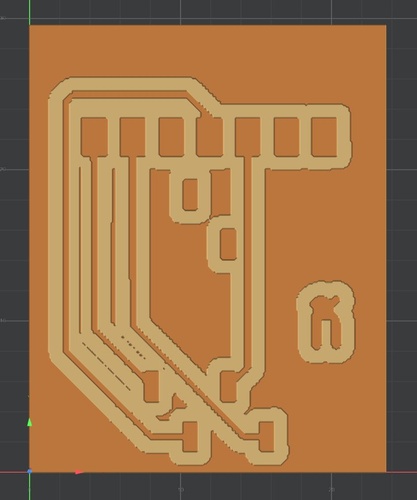
The Mods CE simulation revealed a problem that the KiCad DRC had not caught. The DRC validates electrical rules — minimum clearances between copper features as defined in Board Setup — but it has no knowledge of the physical tool that will cut the board. In the upper section of the layout, several traces were routed close enough together to pass DRC, but not close enough to leave space for the 1/64” endmill to pass between them. The simulation showed those traces merging into a single copper island — a short circuit created by the tool, not by the design.
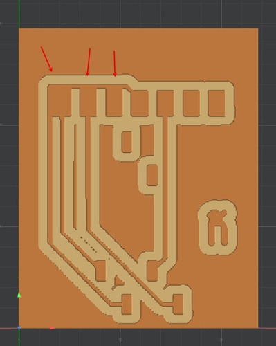
The fix was to go back to the PCB editor, increase the spacing between the affected traces, re-export the Gerbers, regenerate the PNGs in Gerber2PNG, and reload them in Mods. The second simulation confirmed all traces were now properly isolated.
testing.
VL53LXX breakout — wiring and first readings.
With both boards designed and the toolpaths ready, the immediate priority was validating that the VL53LXX breakout communicates correctly over I2C before committing to milling. The wiring to the XIAO RP2040 is straightforward:
| VL53LXX | XIAO RP2040 |
|---|---|
| VCC | 3V3 |
| SDA | D4 (GPIO 6) |
| SCL | D5 (GPIO 7) |
| GND | GND |
SHUT and INT were left unconnected — SHUT controls power-down mode and INT signals when a measurement is ready; neither is needed for basic distance readings.
One thing worth checking before connecting: the breakout almost certainly has pull-up resistors already integrated on the PCB. Measuring between VCC and SDA (and VCC and SCL) with a multimeter confirmed ~4.7 kΩ on each line. This means no external pull-ups should be added — two sets of pull-ups in parallel would halve the effective resistance to ~2.35 kΩ, increasing current draw unnecessarily.
The sketch used is the one provided by Adrián Torres (Fab Lab León, 2023), which uses the VL53L1X library by Pololu — not the Adafruit version. This is an important distinction: both appear in the Arduino IDE library manager under similar names, but their APIs are different. Using the Adafruit library with this sketch produces a compilation error (VL53L1X.h: No such file or directory) because the header name differs.
tab: VL53L1X distance sensor | tof-vl53l1x.ino
//Fab Academy 2023 - Fab Lab León
//Time of Flight VL53L1X
//Fab-Xiao
#include <Wire.h>
#include <VL53L1X.h>
VL53L1X sensor;
void setup()
{
Serial.begin(115200);
Wire.begin();
Wire.setClock(400000); // use 400 kHz I2C
sensor.setTimeout(500);
if (!sensor.init())
{
Serial.println("Failed to detect and initialize sensor!");
while (1);
}
sensor.setDistanceMode(VL53L1X::Long);
sensor.setMeasurementTimingBudget(50000);
sensor.startContinuous(50);
}
void loop()
{
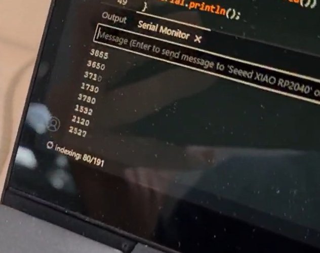
Serial.print(sensor.read());
if (sensor.timeoutOccurred()) { Serial.print(" TIMEOUT"); }
Serial.println();
}tab: end
A note on Wire.begin(): the sketch never explicitly declares which pins are SDA and SCL. This works because Wire.begin() without arguments uses the default I2C pins defined in the XIAO RP2040 BSP (Board Support Package) — D4 for SDA and D5 for SCL. If a different pin pair were needed, Wire.setSDA() and Wire.setSCL() would have to be called before Wire.begin().
The Serial Monitor at 115200 baud prints one distance reading per line every 50 ms. Moving the sensor closer to a surface decreases the value; moving it away increases it. The video below shows the readings changing as the sensor is moved toward and away from a fixed surface.
reflection.
This week pushed me into territory I had not explored properly before. I had used I2C in projects — always through libraries, always treating it as a black box — but I had never actually looked at what happens on the wire. Going through the logic analyzer captures and reading the transactions frame by frame (start condition, 7-bit address, ACK, data bytes, stop) gave me a much more concrete picture of the protocol than any tutorial had.
The oscilloscope work was similarly eye-opening. Measuring the same bus with two instruments — the logic analyzer decoding the digital frames and the DSO Shell showing the analog voltage levels — made it clear why both approaches matter. The logic analyzer tells you what is being communicated; the oscilloscope tells you whether the signal is electrically healthy. The DSO Shell’s bandwidth limitation at 400 kHz I2C was itself instructive: understanding why the measured frequency was ~154 kHz instead of 400 kHz, and why the edges look rounded, turned a frustrating result into a useful data point about instrument selection.
On the design side, this week meant two new KiCad boards from scratch. The TLE493D board deepened the work from Week 06 — same workflow, more considered component choices, and a better understanding of why each passive is there. The VL53LXX adapter board introduced something new: placing footprints at a precise measured distance rather than dragging them by eye. That single technique — opening Footprint Properties and typing a coordinate directly — is the kind of thing that seems obvious in hindsight but takes actually needing it to learn.
What remains pending: milling and soldering the VL53LXX adapter board. The TLE493D magnetometer was ruled out for the final project — sensing absolute position from magnetic field strength does not work over the leg’s 530 mm of travel, as the detection-range note explains — so the ToF breakout adapter is the design that moves forward into fabrication.
files.
TLE493D magnetometer board
VL53LXX ToF adapter board