Electronics design
weekly schedule.
| Time block | Wed | Thu | Fri | Sat | Sun | Mon | Tue | Wed |
|---|---|---|---|---|---|---|---|---|
| Global class | 3 h | |||||||
| Local class | 1,5 h | 1.5 h | ||||||
| Research | 2 h | 2 h | 1 h | |||||
| Design | 3 h | 2 h | ||||||
| Fabrication | ||||||||
| Documentation | 2 h | 1h | 1 h | 4 h | ||||
| Review |
background.
Electronics has been part of my training since university. During my engineering degree I worked extensively with circuit simulation — I ran my first electrical circuit simulations in PSpice, which gave me a solid foundation for understanding component behaviour before building anything physical. That said, the transition from schematic simulation to PCB design and physical fabrication is a different discipline, and this week was my first structured exposure to the full pipeline.
On the measurement side, the multimeter is a tool I use daily in my professional work as an automation and robotics engineer. Continuity checks, voltage verification, and basic component testing are routine tasks on industrial control systems, so that part of this week felt immediately familiar.
overview.
This week is about electronics design — taking a circuit idea all the way from schematic to a fabrication-ready PCB using an EDA tool. Coming from an automation and robotics background, I deal with PLCs and pre-built boards every day, but I have never actually designed my own PCB from scratch. So this is genuinely new territory for me.
I used KiCad 9 (the CERN-backed open-source EDA tool) to design a simple development board around the Seeed XIAO RP2040 — the same microcontroller I have been working with since Week 04. The board has a socket for the XIAO, an LED with a current-limiting resistor, a tactile button with a pull-down resistor, and open header pins for future expansion. Simple on paper, but the real learning is in the process itself: understanding ERC errors, figuring out trace routing by hand, exporting the fabrication files correctly, and navigating the frankly unintuitive mods Project interface to generate toolpaths for the Roland MDX-20.
learning objectives.
- Understand the full PCB design workflow: schematic → layout → fabrication files
- Learn to use KiCad 9 (schematic editor, PCB editor, ERC, DRC)
- Use the Fab Lab component libraries for KiCad
- Understand what ERC and DRC check and why they matter
- Generate fabrication-ready files (Gerber → PNG) for PCB milling
- Prepare toolpaths with mods Project for the Roland MDX-20
- Use test equipment to observe microcontroller operation (group assignment)
- Simulate a circuit
assignments.
- Group assignment: Use the test equipment in the lab to observe the operation of an embedded microcontroller circuit (multimeter, oscilloscope, logic analyzer minimum).
- Individual assignment — Simulate a circuit.
- Individual assignment — Design an embedded microcontroller system using parts from the Fab inventory, check design rules for fabrication.
- Extra credit: try another design workflow.
- Extra credit: design a case.
group assignment — test equipment.
For the group assignment, we need to demonstrate the use of test equipment on a microcontroller circuit board. I am documenting the instruments I will be working with. The actual testing will happen once the board is fabricated in Week 08 (Electronics Production).
→ Fab Lab León 2026 Group Page.
multimeter — Fluke 179 True RMS.

This is my personal multimeter. I bought it years ago and it has been my daily instrument in the field — verifying motors, checking power distribution panels, debugging industrial control systems. It is the kind of tool you learn to trust.
| Feature | Specification |
|---|---|
| DC voltage | 0.1 mV – 1000 V |
| AC voltage | 0.1 mV – 1000 V (True RMS) |
| DC/AC current | 0.01 mA – 10 A |
| Resistance | 0.1 Ω – 50 MΩ |
| Capacitance | 1 nF – 9999 μF |
| Temperature | -40 °C – 400 °C |
| Safety rating | CAT III 1000 V, CAT IV 600 V |

I want to highlight the CAT III/IV rating specifically. In automation and robotics consulting, I frequently need to verify voltages on motors, power distribution lines, and control cabinets running at 380 V and 400 V AC. Having probes rated for those voltages is a safety requirement, not a luxury.
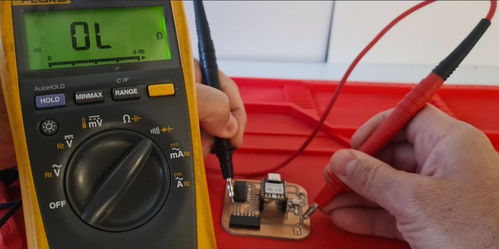
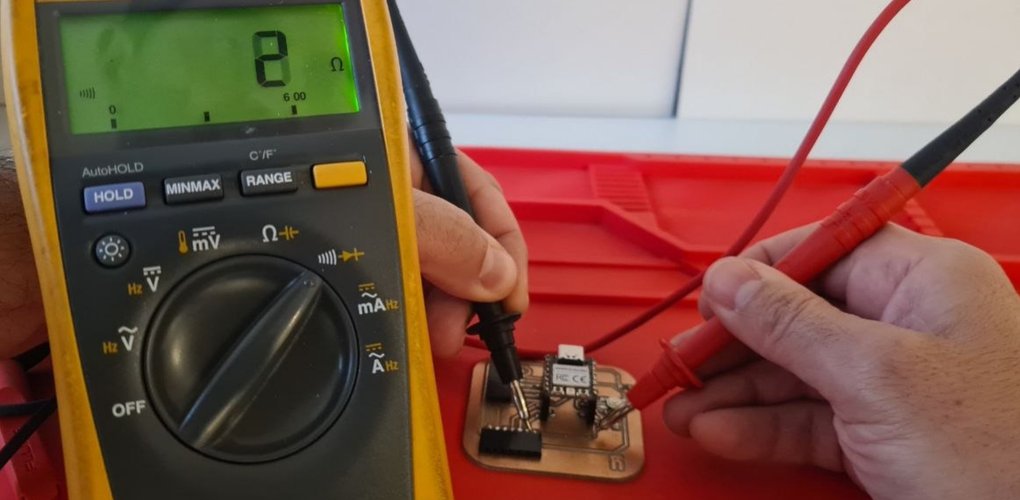
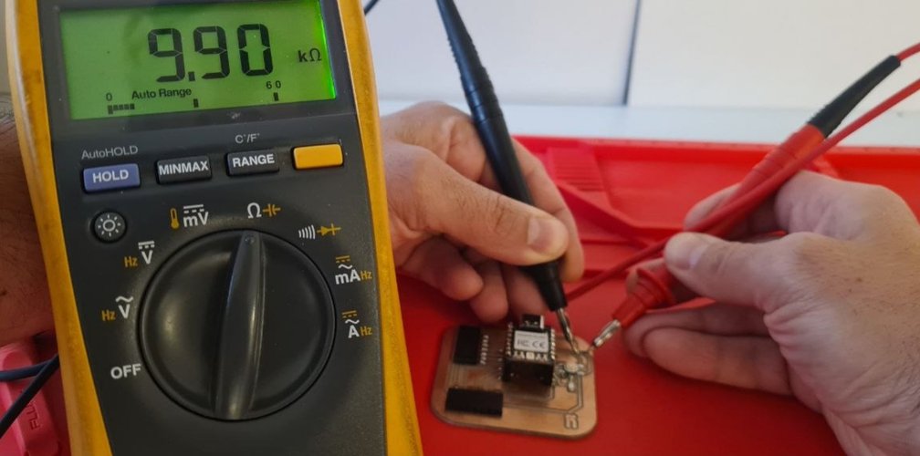
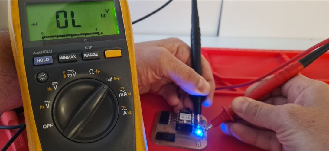
testing and measurements with multimeter.
I performed several measurements on my XIAO RP2040 board with a digital multimeter: continuity on traces and solder joints, resistance, and diode-check to verify the integrated LED. The key ones are shown below as still photos. On the Fluke 179 the mode is chosen with the rotary dial; continuity and diode-check share a position and are toggled with the yellow button.
I also measured the current drawn by a blinking LED on an Arduino, where the reading changes as the LED switches on and off:
Measuring the current of a blinking LED driven by an Arduino with the multimeter.
This hands-on testing helped me understand the practical challenges of characterizing integrated modules versus discrete components.
oscilloscope — DSO Shell (DIY kit).


An oscilloscope displays electrical signals as waveforms: voltage on the vertical axis, time on the horizontal. Unlike a multimeter, which gives you a single static reading, an oscilloscope shows how a signal behaves over time — its shape, frequency, amplitude, and duty cycle. That makes it the right tool for anything involving PWM, communication protocols, or any signal that changes faster than a display can follow.
The DSO Shell at Fab Lab León is a pocket unit assembled from a DIY soldering kit. It runs on a 9 V battery and has limited bandwidth compared to a bench instrument, but it is fully adequate for inspecting microcontroller-level signals.
what do we expect to see?
PWM (Pulse Width Modulation) does not actually vary the voltage on a pin — it varies the proportion of time the pin spends at its high logic level within each cycle. At 1 kHz, the pin switches on and off 1000 times per second. The RP2040 operates at 3.3 V logic, so the pin alternates between 0 V and 3.3 V at that rate. The LED cannot respond fast enough to each individual pulse, so it perceives the average — which is why it appears to fade smoothly even though the pin is always either fully on or fully off.
On the oscilloscope screen we therefore expect to see a rectangular wave — clean vertical edges, a flat top at ~3.3 V, a flat bottom at 0 V — and the width of the high pulse changing continuously as the duty cycle ramps up and down. The carrier frequency should read close to 1000 Hz, and the Vpp should be close to 3.3 V.
verifying the setup in Thonny.
Before connecting the oscilloscope, I went through a few steps to confirm the signal was actually present on the target pin.
Step 1 — Confirm the interpreter. In Thonny, Tools → Options → Interpreter must be set to MicroPython (RP2040) on the correct COM port. The status bar at the bottom of the window confirms this.
Step 2 — Check available pins. With no datasheet for the Qpad immediately at hand, I queried the board directly from the Thonny shell:
from machine import Pin
print(dir(Pin.board))  # lists all GPIO names exposed by the firmware
This returned all GPIO names available on the firmware, confirming GP26 (D0) was present and unassigned.
Step 3 — Verify PWM on the target pin. Before running the full fading loop, I sent a static 50 % duty cycle to GP26 to confirm the pin was functional:
from machine import Pin, PWM

p = PWM(Pin(26))      # assign PWM peripheral to GP26 (physical pad D0)
p.freq(1000)          # set carrier frequency to 1 kHz
p.duty_u16(32768)     # 32768 out of 65535 = 50 % duty cycle
print("OK")           # confirm execution reached this line
The shell returned OK and the LED lit at half brightness — confirming the pin was outputting PWM correctly.
Step 4 — Run the fading script. Once the static test passed, I loaded the full script:
from machine import Pin, PWM
from time import sleep

led = PWM(Pin(26))    # assign PWM to GP26 — D0 header pin, accessible with a probe

led.freq(1000)        # 1 kHz carrier: 1000 on/off cycles per second

while True:
    # ramp duty cycle up from 0 % to 100 %
    for duty in range(0, 65536, 512):      # 65535 = full on in MicroPython's u16 scale
        led.duty_u16(duty)                 # update duty cycle
        sleep(0.01)                        # wait 10 ms before next step

    # ramp duty cycle back down from 100 % to 0 %
    for duty in range(65536, 0, -512):
        led.duty_u16(duty)
        sleep(0.01)
The LED faded smoothly and continuously. With the signal confirmed active on D0, the oscilloscope probes could be connected with confidence.
measurement.
The board used is the Qpad — a didactic game pad built around the XIAO RP2040, developed at CBA MIT. The black probe goes to a GND pad on the board; the red probe to the D0 header pin on the XIAO.
The DSO Shell was configured at 1 V/div vertically and 0.2 ms/div horizontally.
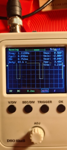
| Parameter | Measured | Expected |
|---|---|---|
| Frequency | 1.112 kHz | 1.000 kHz |
| Period | 0.898 ms | 1.000 ms |
| Vpp | 3.40 V | 3.30 V |
| Duty cycle | 83.6 % | 0–100 % (sweeping) |
| Vrms | 1.21 V | — |
is this coherent with what we expected?
Yes, completely. The waveform is a clean rectangular wave — confirming the pin switches fully between its two logic states with no intermediate levels, exactly as PWM requires.
The frequency reads 1.112 kHz against the 1000 Hz set in code. The discrepancy comes from the overhead of the MicroPython interpreter executing the sleep() calls and the loop itself, which adds a few microseconds per cycle. This is normal and expected when generating PWM this way in MicroPython.
The Vpp of 3.40 V against the nominal 3.3 V of the RP2040 is within the DSO Shell’s calibration tolerance — a 3 % deviation is entirely acceptable for this instrument.
The duty cycle of 83.6 % simply reflects the exact moment in the fading sweep at which the oscilloscope triggered. Had the screenshot been taken a moment earlier or later it would show a different value — which is precisely the point: the duty cycle is what the code is changing continuously, and the oscilloscope captures it at one instant.
All observations are consistent with the code, with the expected behaviour of PWM, and with the visual result seen on the LED.
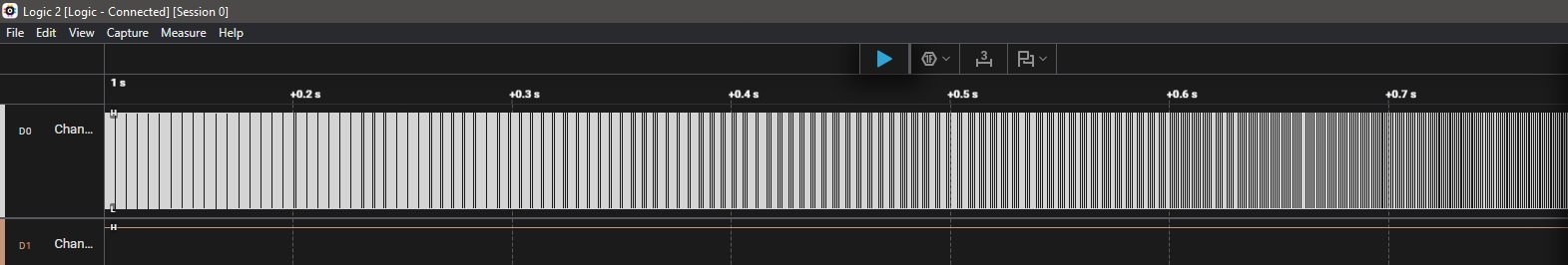
DSO Shell measuring the PWM output on pin D0 of the Qpad (XIAO RP2040). The waveform shifts as the duty cycle changes during the fading cycle.
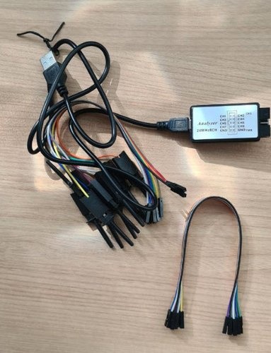
logic analyzer — 24 MHz 8-channel.
A logic analyzer captures digital signals over time and displays them as timing diagrams. Unlike an oscilloscope, which measures voltage as a continuous analogue value, a logic analyzer only resolves high and low states — but it does so with high timing precision and can decode communication protocols (I2C, SPI, UART) automatically. For a PWM signal, the key advantage over the oscilloscope is the ability to capture several seconds of data and see how the duty cycle evolves across the entire recording.
The unit at Fab Lab León is a generic 8-channel USB device compatible with the Saleae Logic 2 software (version 2.4.42). It connects to the computer via USB and requires no external power.
setup in Logic 2.
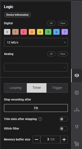
Configuration used:
- Sample rate: 12 MS/s (closest available to the recommended 10 MS/s)
- Capture mode: Timer — 3 seconds
- Analyzers: none — PWM is not a serial protocol, so no decoder is needed
- Channel: D0 only (CH0 on the logic analyzer)
- Glitch filter: enabled
Connections are identical to the oscilloscope: CH0 cable to D0, GND cable to a GND pad on the Qpad.
capture results.
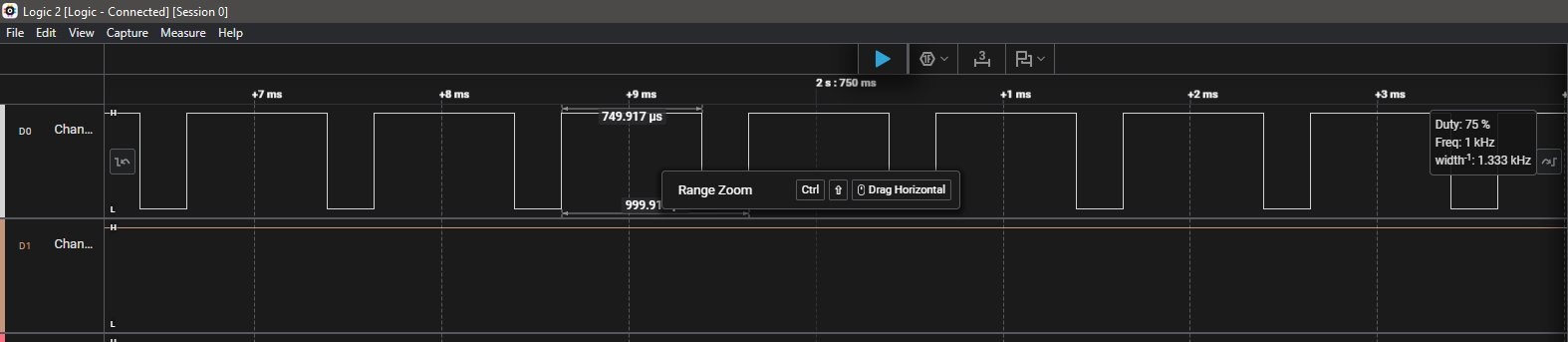
Logic 2 capturing the PWM output on pin D0 of the Qpad (XIAO RP2040). The full 3-second timeline shows the duty cycle sweeping continuously as the fading script runs.
oscilloscope vs logic analyzer — same signal, two perspectives.
Both instruments measured the same PWM signal on pin D0. The results are consistent and complementary:
| Parameter | DSO Shell (oscilloscope) | Logic 2 (logic analyzer) |
|---|---|---|
| Frequency | 1.112 kHz | 1.000 kHz |
| Period | 0.898 ms | 0.999 ms |
| Duty cycle | 83.6 % | 75 % |
| Vpp | 3.40 V | — (digital only) |
| Timeline view | Single frame | Full 3 s sweep |
The duty cycle and frequency differ between the two readings because each instrument captured a different moment in the fading sweep — the duty cycle is continuously changing, so any two snapshots will show different values. Both are correct for their respective instants.
The oscilloscope provides the voltage dimension — confirming the signal swings between 0 V and 3.3 V as expected. The logic analyzer provides the time dimension — the overview capture makes it immediately visible that the pulse width is sweeping across the full recording, something the oscilloscope cannot show in a single frame.
Neither instrument alone tells the complete story. Together they give a full characterisation of the signal.
individual assignment — PCB design with KiCad.
setting up KiCad 9 and the Fab libraries.
First step: install KiCad 9 and import the Fab Lab component libraries. These libraries contain symbols and footprints for the components available in the Fab inventory, which ensures whatever I design can actually be built with what we have in stock. The installation process follows the Fab Academy KiCad tutorial.
One important detail: when searching for components in the schematic editor, I had to make sure I was looking inside the Fab library folders specifically, not the default KiCad libraries. The Fab footprints match the actual parts we have.
schematic design — first iteration.
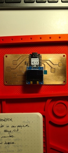
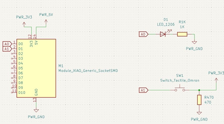
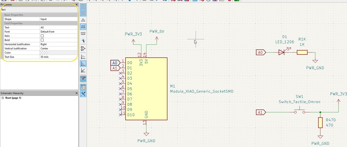
My board follows the minimum requirements for this week: a XIAO RP2040 on a socket, one LED, one tactile button, and open pins for future use. The circuit is straightforward:
- M1:
Module_XIAO_Generic_SocketSMD— the XIAO socket from the Fab library - D1:
LED_1206— a 1206-package LED connected to pin D0 - R1: 1 kΩ resistor — current limiting for the LED (calculated for ~2 mA at 3.3 V with a ~1.8 V forward drop)
- SW1:
Switch_Tactile_Omron— a tactile push button connected to pin D1 - R2: 470 Ω resistor — pull-down for the button
A couple of things I got wrong on this first pass that Claude pointed out during our design session:
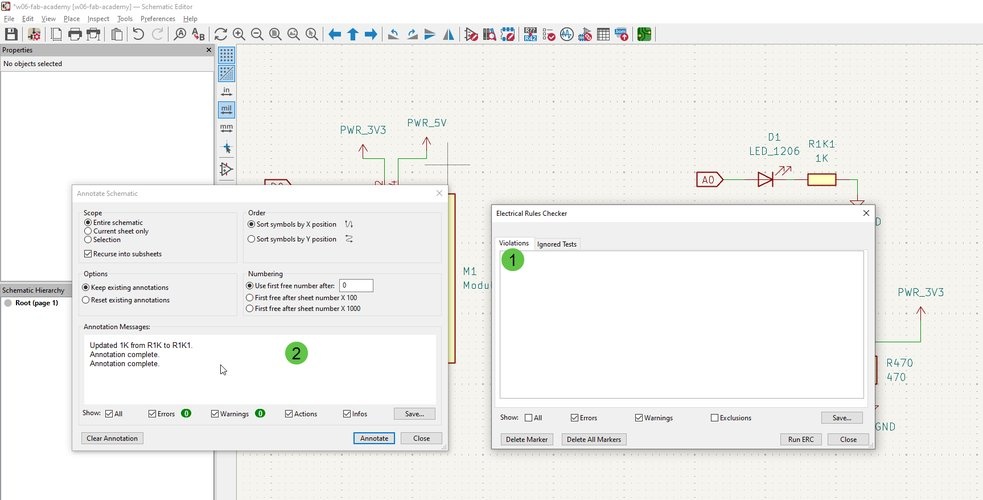
Resistor naming. I initially named the 1 kΩ resistor R1K, which is not standard EDA practice. The convention is to use a sequential reference designator (R1, R2, R3…) and put the value separately. KiCad’s annotation tool later caught this and renamed it to R1K1, which is still ugly. I ended up fixing it to just R1 with a value of 1K.
Unused pins need no-connect flags. Pins D2 through D10 are intentionally unused in this design, but KiCad does not know that. Without explicit no-connect flags (the X symbol), the ERC will flag every single one as an unconnected pin warning. In KiCad 9, you place them via Place → No Connect Flag or the shortcut Q.
running the ERC — and learning from the errors.
The Electrical Rules Check is where things got interesting. I ran it and got a wall of violations.
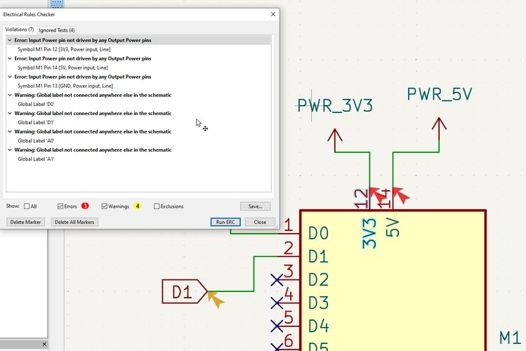
The 4 warnings were about global labels (D0, D1, A0, A1) not being connected elsewhere in the schematic — single-sheet design, used once. Not a real problem.
The 3 errors were more puzzling: “Input Power pin not driven by any Output Power pins” on the XIAO’s 3V3 (pin 12), 5V (pin 14), and GND (pin 13). What does this even mean?
Claude’s explanation: The XIAO symbol in the Fab library defines 3V3, 5V, and GND as Power Input pins. KiCad expects every Power Input pin to be driven by a corresponding Power Output pin somewhere in the schematic. But since the XIAO generates these voltages internally from USB, there is no explicit Power Output pin in my schematic feeding those nets. The ERC sees undriven power rails and flags them as errors.
The fix: add a PWR_FLAG symbol to each of these nets. PWR_FLAG tells the ERC that the net is indeed powered. It is annotation-only — it does not add any physical component to the board.
This was a genuine “aha” moment. The circuit works perfectly fine without the flags, but understanding why the ERC complains — and resolving it properly instead of just ignoring the errors — felt like the right approach.
final schematic.
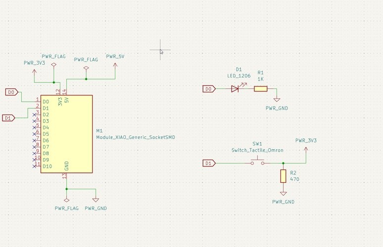
The final schematic includes all the fixes: PWR_FLAG on the three power nets, no-connect flags on all unused XIAO pins, and properly named components. The ERC passes clean.
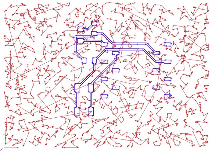
PCB layout — manual routing.
Moving from schematic to PCB layout, the first thing I did was set up the track widths in Board Setup → Design Rules → Pre-defined Sizes: 0.4 mm (standard for Fab Academy boards milled with a 1/64” endmill) and 0.8 mm as a wider option. In practice, I routed everything at 0.4 mm.
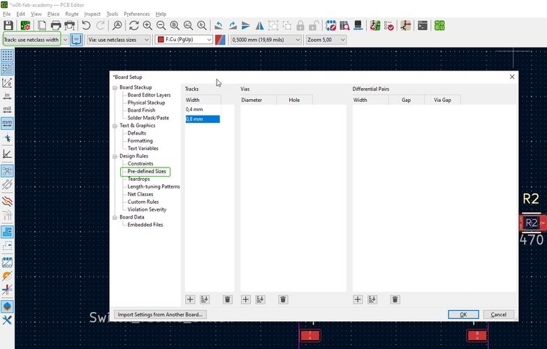
I routed every trace manually — no autorouter. The principle is straightforward: keep traces as short and direct as possible. Less resistance, cleaner signal paths, and easier to mill. With only a handful of components, the routing was manageable, though I had to think carefully about physical placement to avoid crossings on a single-layer board.
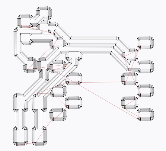
design rules check (DRC).
Once the layout was complete, I ran the DRC with “Test for parity between PCB and schematic” enabled. This checks not only physical design rules (minimum clearances, track widths) but also verifies that the PCB matches the schematic — no missing connections, no extra traces.
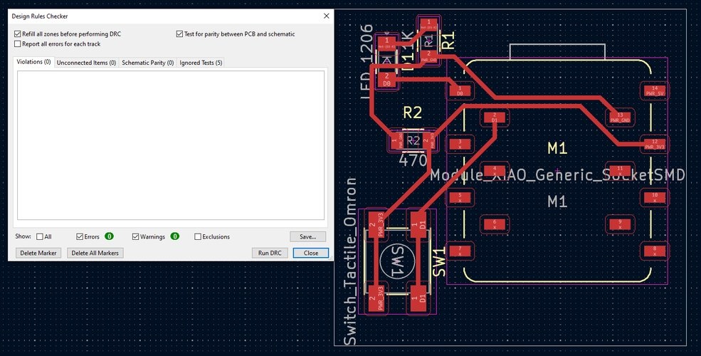
Clean. Zero violations, zero unconnected items, zero schematic parity errors.
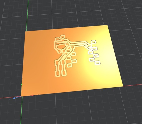
exporting fabrication files.
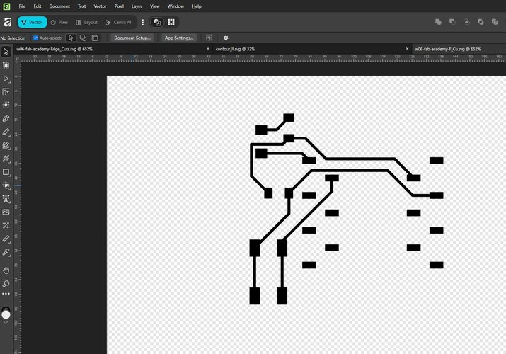
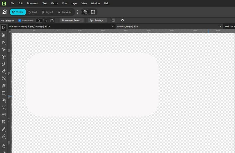
My first attempt was to export SVGs — one for the copper traces (F.Cu layer) and one for the board outline (Edge.Cuts layer) — and feed those straight into mods. I went to File → Plot and configured the SVG export:
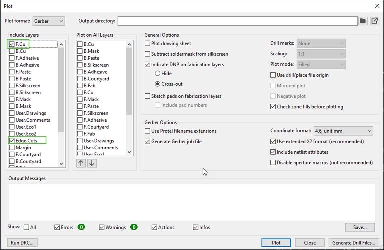
I opened the exported SVGs in Affinity to check them:
The actual workflow at Fab Lab León is Gerber → PNG, not SVG. Once the PCB design is finished in KiCad, I export the Gerbers (including the drill file if the board has through-holes) and convert them to PNG with gerber2png.fablabkerala.in: upload the Gerbers, select Black and White, and hit Generate All. That produces the trace and outline PNGs that mods needs.
verifying toolpaths with mods.
mods Project is a web-based tool for generating machine toolpaths. It is… not the most intuitive interface I have ever used. The entire thing is a visual node-based pipeline where you connect processing modules with cables. Powerful in concept, overwhelming in practice when you first open it.
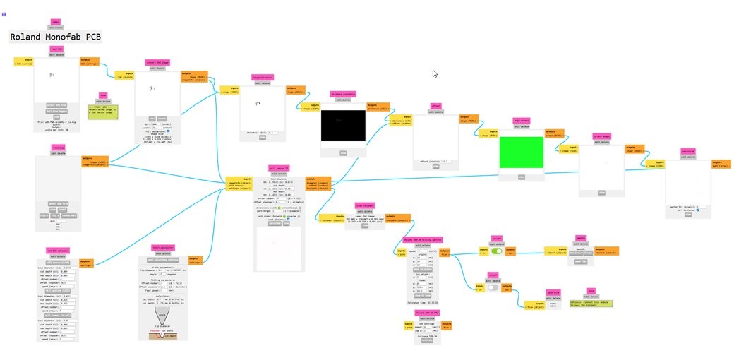
Before going further, I wanted to verify the toolpath visually — roughly like a slicer preview in 3D printing. I loaded the PNG exported from the Gerber file (converted using gerber2png.fablabkerala.in) into mods and the result was completely wrong.
My instructors and I spent time troubleshooting — different export settings, different mods configurations. Nothing resolved it. The breakthrough came during a session with Nuria (one of the local instructors): she shared a PNG that had previewed correctly on her laptop, I loaded it on mine, and it was still broken. At that point I noticed the mods interface had changed slightly — it looked like the tool had been updated. On a hunch, I tried Firefox instead of Brave.
Brave is built on Chromium — the same open-source engine that powers Chrome — yet Chrome rendered mods correctly while Brave did not. The most likely explanation involves Brave’s aggressive privacy features, which by default can intercept or modify WebAssembly execution and canvas-based rendering. mods relies heavily on both for its toolpath computation. Maybe disabling Brave Shields for the mods domain could likely resolve it, but I have not confirmed this. For now, Firefox or Chrome are the verified browsers for running mods at Fab Lab León.
The milling parameters are configured in the “set PCB defaults” module:
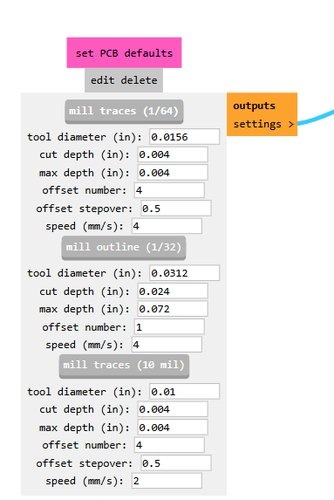
| Profile | Tool diameter | Cut depth | Max depth | Offsets | Speed |
|---|---|---|---|---|---|
| Mill traces (1/64”) | 0.40 mm | 0.10 mm | 0.10 mm | 4 | 4 mm/s |
| Mill outline (1/32”) | 0.79 mm | 0.61 mm | 1.83 mm | 1 | 4 mm/s |
| Mill traces (10 mil) | 0.25 mm | 0.10 mm | 0.10 mm | 4 | 2 mm/s |
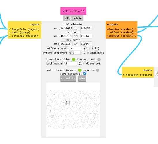
The mill raster 2D module is where you hit Calculate to generate the toolpath:
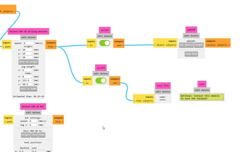
sending the toolpath to the MDX-20.
With the MDX-20 there is no .rml file to download: the toolpath is sent to the machine directly over a serial connection. mods does this through its WebSerial output, which only works reliably in Chrome (the Chromium-based Brave does not). With the Roland connected by its RS-232 serial cable and its driver installed, I open the WebSerial connection in mods, select the Roland’s serial port, and the calculated toolpath is sent straight to the machine.
The actual milling will happen in Week 08 — Electronics Production.
workflow diagram.
After going through this entire process, I want to leave a clear reference for my future self. This is the complete flow from idea to fabrication-ready files:
flowchart TD
    A["Install KiCad 9 + Fab Libraries"] --> B["Schematic Editor"]
    B --> B1["Place components from Fab library"]
    B1 --> B2["Wire connections"]
    B2 --> B3["Add PWR_FLAG to power nets"]
    B3 --> B4["Add no-connect flags to unused pins"]
    B4 --> B5["Run Annotate"]
    B5 --> C["Run ERC"]
    C -->|Errors| B
    C -->|Clean| D["PCB Editor"]
    D --> D1["Set track widths — Board Setup\n0.4 mm for 1/64 inch endmill"]
    D1 --> D2["Place and arrange components"]
    D2 --> D3["Route traces manually"]
    D3 --> D4["Draw board outline — Edge.Cuts"]
    D4 --> E["Run DRC with schematic parity"]
    E -->|Errors| D
    E -->|Clean| F["Export Gerbers — Fabrication Outputs"]
    F --> F1["Traces — F.Cu layer"]
    F --> F2["Outline — Edge.Cuts layer"]
    F1 --> FP["Generate trace + outline PNGs\n(gerber2png)"]
    F2 --> FP
    FP --> G["mods Project — Roland MDX-20 PCB pipeline"]
    G --> G1["Load PNGs into mods"]
    G1 --> G2["Select tool profile\n1/64 in traces · 1/32 in outline"]
    G2 --> G3["Calculate toolpath"]
    G3 --> H["Send toolpath to MDX-20 via Serial"]
    H --> I["Mill on Roland MDX-20\nWeek 08"]

    style A fill:#0FD9B0,stroke:#0a8a6e,color:#000
    style I fill:#0FD9B0,stroke:#0a8a6e,color:#000
simulation (extra credit).
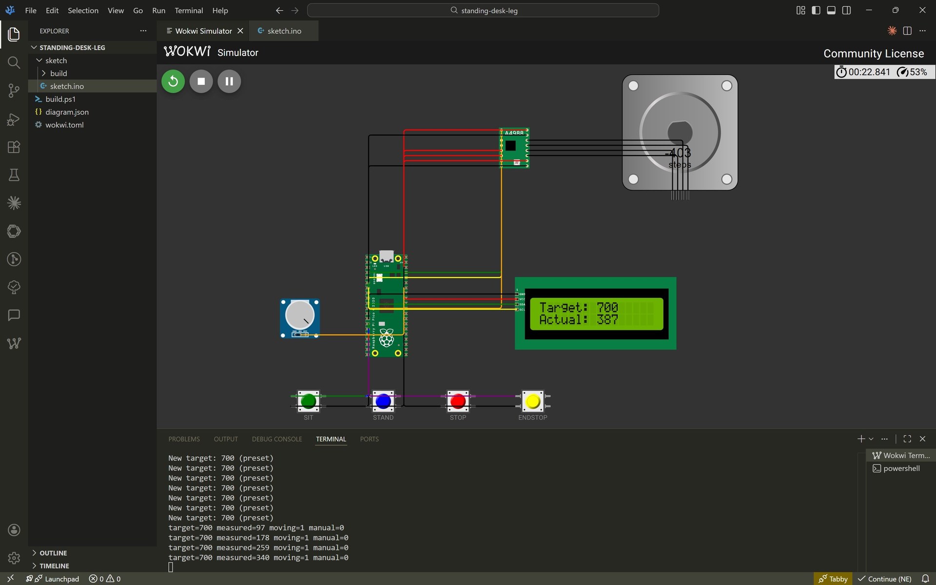
The week’s extra credit asks for a simulation of the designed board. Rather than simulate the VL53L0X adapter in isolation — which wouldn’t show much beyond a fixed reading — I built a simulation that models one telescopic leg of the final project, closing the loop between the microcontroller, the stepper driver, the motor, and a position sensor.
The final project is a height-adjustable standing desk with four telescopic legs. Each leg is driven by a XIAO RP2040 controlling a NEMA 17 stepper through a TMC2209 silent driver, with a VL53L0X ToF sensor for absolute position feedback. A Waveshare ESP32-S3 touchscreen coordinates the four legs over UART. The simulation below models a single leg of that system.
simulation platform — Wokwi.
I used Wokwi because it simulates the RP2040 microcontroller accurately (same RP2040js engine, same Arduino-Pico core that will run on the real XIAO RP2040) and has native support for stepper motors, drivers, I²C displays and standard input components. The whole simulation is reproducible from two files: diagram.json (the wiring) and sketch.ino (the firmware).
A note on board choice.Wokwi does not support the XIAO RP2040 in its board library. I used the Raspberry Pi Pico as a proxy, since both boards share the same RP2040 microcontroller and the same Arduino-Pico core. The sketch compiles and runs identically on either board — only the pin mapping needs adjustment when deploying to the real XIAO.
from the web IDE to VSCodium.
My first attempt was the Wokwi web IDE. It was the fastest way to get started — paste the sketch, paste the diagram, press Play. But as soon as I started iterating on the design, the free-tier build servers became a hard bottleneck. Each recompile triggered this dialog:
Build Servers Busy — Your project compilation is taking longer than expected. Perhaps our build servers are too busy right now. You can try to compile the project on your computer and simulate it using Wokwi for VS Code, or upgrade to a paid plan to skip the build queue.
Retrying three times for every change was not workable. I followed Wokwi’s own suggestion and moved to the Wokwi for VS Code extension, installed inside VSCodium. The extension ships with the simulator but delegates compilation to a local toolchain — in my case, the same Arduino-Pico core I’ll use for the real XIAO build. Compiles are now instant, the simulation launches inside the editor, and I stopped depending on remote server availability. As a side effect, I also have my final-project toolchain fully set up well before I need it.
The end of this section documents how to reproduce the simulation both on the Wokwi web and on the local VSCodium setup.
what the simulation models.
| Real hardware | Wokwi proxy | Notes |
|---|---|---|
| XIAO RP2040 | Raspberry Pi Pico | Same RP2040, same core |
| TMC2209 driver | A4988 driver | Both use identical STEP/DIR/ENABLE interface |
| NEMA 17 motor | Bipolar stepper | Visually rotates with step counter |
| VL53L0X ToF sensor | Internal step counter | See note on position feedback below |
| Endstop switch | Pushbutton | Resets position to 0 |
| Touchscreen UI | 3 pushbuttons + I²C LCD | SIT, STAND, STOP + live target/actual readout |
| Manual fine-adjust | Potentiometer with deadband | Overrides presets when moved past a threshold |
The position scale is abstracted to a 0–1000 range for visual clarity — the real machine runs on absolute millimetres (sit ≈ 720 mm, stand ≈ 1250 mm, stroke ≈ 530 mm). The tolerance band (±2 units in the simulation, ±2 mm in the real build) is preserved.
Position feedback — simulated vs real.On real hardware, the VL53L0X ToF sensor measures the actual leg height directly. In this simulation, the measured position is computed internally by counting the STEP pulses sent to the driver — each step increments the position by one unit in the current direction. This keeps the control logic identical (target, error, tolerance band, stop) while making the motion visible without external interaction. On real hardware, the only line that changes is where
measuredPoscomes from: an internal counter here,tof.readRangeSingleMillimeters()from the VL53L0X on the board.
control logic.
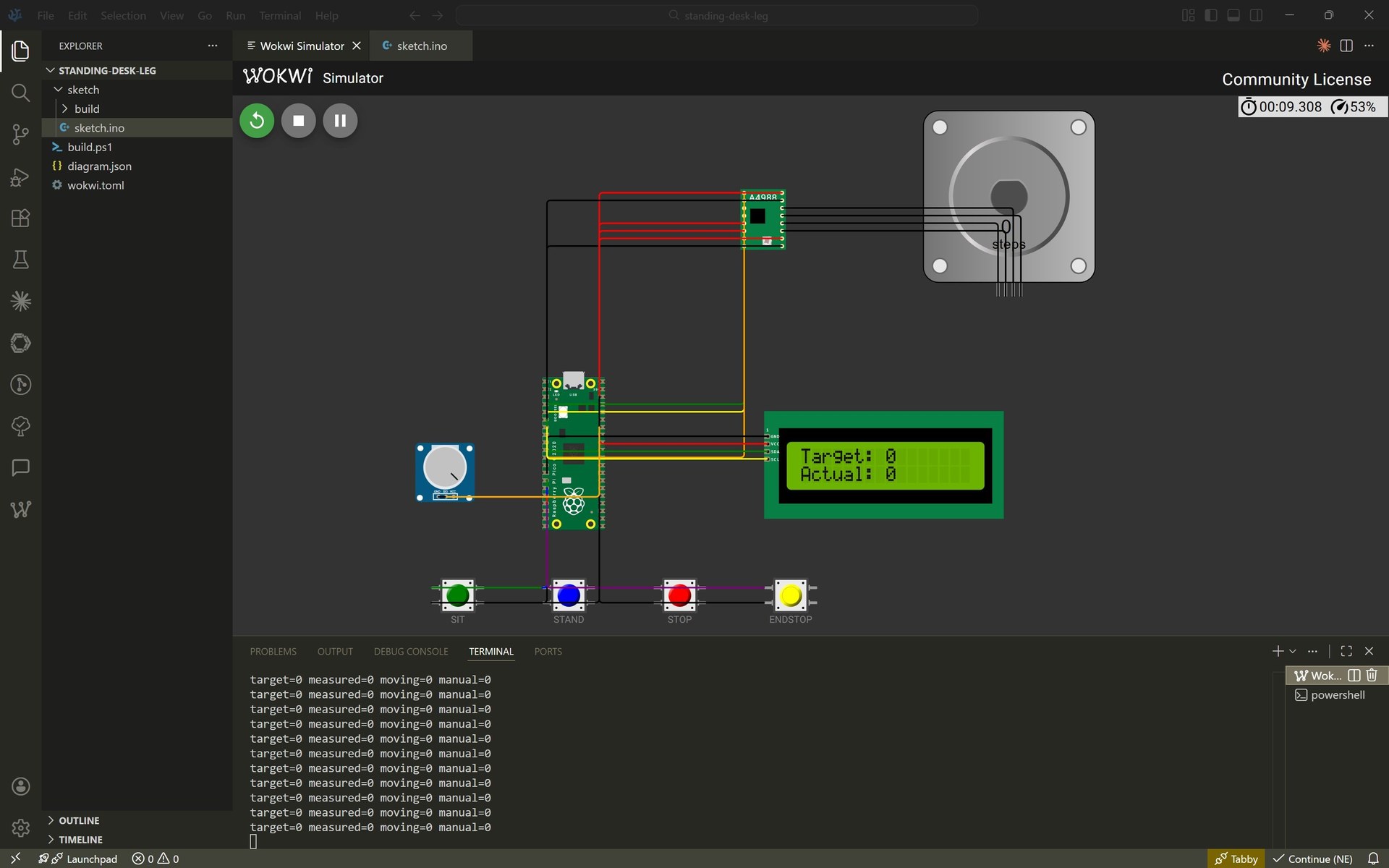
- Preset buttons. SIT sets the target to 200, STAND sets it to 700, STOP halts motion and disables the driver. ENDSTOP resets the measured position to 0 (simulates the homing switch at the bottom of the telescopic leg).
- Manual fine-adjust (potentiometer). When the potentiometer moves more than
POT_DEADBANDunits (15) from its last accepted reading, it overrides the preset and becomes the new target. The LCD shows anMmarker next to the target when manual mode is active. The deadband is essential — without it, ADC noise would constantly retrigger the target and the motor would jitter between nearby values instead of settling. - Closed-loop motion. On every iteration, the sketch compares the measured position to the target. If the difference exceeds the tolerance band, it steps the motor in the appropriate direction and increments the simulated position. Once within ±2 units, it stops and disables the driver.
- Display. A 16×2 I²C LCD shows the current target and measured position, refreshed at 10 Hz to avoid flicker.
Movement profile is constant velocity. Acceleration ramps with AccelStepper (trapezoidal profile) are planned for the Week 10 output-devices work, where they actually matter — on real hardware, a 100 kg desktop starting from rest at full speed would skip steps immediately.
wiring.
behaviour during the simulation.
how to run it.
There are two ways to reproduce the simulation.
tab: Option A — Wokwi web (fastest)
Open the published project and press Play:
→ Standing desk leg controller on Wokwi
Press SIT or STAND and watch the motor move the measured position toward the target. Press STOP at any point to halt. Press ENDSTOP (yellow) to reset the position to 0. Move the potentiometer past the deadband to take manual control — the M marker appears on the LCD.
Expect occasional “Build Servers Busy” messages on the free tier. If that happens, use the local VSCodium setup below.
tab: Option B — Local with VSCodium
Reproducing the simulation locally removes the build-queue dependency entirely.
Requirements:
- Arduino CLI installed and in
PATH. - Arduino-Pico core:
arduino-cli config add board_manager.additional_urls https://github.com/earlephilhower/arduino-pico/releases/download/global/package_rp2040_index.json arduino-cli core update-index arduino-cli core install rp2040:rp2040 - LiquidCrystal I2C library (the Arduino IDE and CLI keep separate library folders — install in both if needed):
arduino-cli lib install "LiquidCrystal I2C" - Wokwi for VS Code extension — installed and licensed (
F1→Wokwi: Request a new License).
Project layout:
standing-desk-leg/
├── sketch/
│   └── sketch.ino
├── diagram.json
├── wokwi.toml
└── build.ps1
Compile from the project root, then launch the simulator:
.\build.ps1
# then F1 -> Wokwi: Start Simulator
The simulation panel opens inside VSCodium with the Serial Monitor in the bottom terminal panel, next to a regular PowerShell.
tab: end
prompt used to scaffold the project.
The first version of the sketch and the diagram.json were scaffolded with an AI assistant. After that I iterated on them manually — fixing the I²C pins, adding the A4988 configuration pins, reworking the control paradigm from closed-loop-against-pot to autonomous-with-manual-override, adjusting the ADC scale factor. The final files bear little resemblance to the initial scaffold, but the scaffold removed the boilerplate and let me focus on the actual design decisions.
This is the prompt I sent:
You are helping me build a Wokwi simulation of one telescopic leg of a height-adjustable standing desk for my Fab Academy 2026 Week 06 extra credit. The final project uses a XIAO RP2040, a TMC2209 driver, a NEMA 17 stepper, and a VL53L0X ToF sensor. Wokwi does not support the XIAO RP2040, so use the Raspberry Pi Pico as a proxy. Produce:
- A Wokwi
diagram.jsonthat wires the Pi Pico to a generic A4988 driver (as a stand-in for the TMC2209, same STEP/DIR interface), a bipolar stepper motor, an I2C 16×2 LCD, three pushbuttons labelled SIT / STAND / STOP, an endstop pushbutton, and a potentiometer for manual fine adjust. - An Arduino sketch (
sketch.ino) that:- Models the leg position on a 0–1000 abstract scale (0 = fully collapsed, 1000 = fully extended). Presets: SIT = 200, STAND = 700.
- Tolerance band ±2 units around the target (mirrors the ±2 mm inter-leg tolerance of the real desk).
- Computes the measured position internally by counting STEP pulses (no live sensor in the simulation). Document clearly that the real build replaces this with a VL53L0X read.
- Uses the potentiometer as a manual override: when it moves more than a deadband (~15 units on the 0–1000 scale), its value becomes the new target. Display an 'M' marker on the LCD when manual mode is active.
- Pick I²C pins from the RP2040 I2C0 bus (not I2C1) so the default
Wireobject works. - Tie the A4988 RESET, SLEEP and MS1/MS2/MS3 explicitly in the diagram — floating inputs prevent the driver from stepping in the Wokwi model.
- Write serial debug traces every 500 ms with target, measured, moving flag and manual flag.
A reproducible prompt like this produces a much more targeted scaffold than something vague like “make an Arduino simulation for a standing desk”. The constraints I already knew — XIAO not supported in Wokwi, A4988 as TMC2209 stand-in, I2C0 pin restriction, A4988 configuration pins — went straight into the prompt to save iteration time.
lessons learned — debugging the simulation.
Getting the simulation to run took more debugging than I expected. Two issues in particular are worth documenting because they aren’t obvious from the Wokwi docs and I couldn’t find clear answers in the community forums.
1. I²C pins must match the RP2040 hardware bus mapping.
My first version had SDA on GP6 and SCL on GP7. The sketch booted, the serial monitor printed Setting up I2C... and then hung — Initializing LCD... never appeared, and the LCD stayed blank.
The RP2040 has two I²C peripherals, I2C0 and I2C1, each mapped to specific GPIO pins:
| Bus | SDA options | SCL options |
|---|---|---|
| I2C0 | GP0, GP4, GP8, GP12, GP16, GP20 | GP1, GP5, GP9, GP13, GP17, GP21 |
| I2C1 | GP2, GP6, GP10, GP14, GP18, GP26 | GP3, GP7, GP11, GP15, GP19, GP27 |
The Arduino-Pico Wire object defaults to I2C0. GP6/GP7 belong to I2C1. Calling Wire.setSDA(6) on the default Wire object doesn’t reroute the bus — it silently fails because GP6 isn’t a valid SDA pin for I2C0. Moving SDA/SCL to GP4/GP5 fixed it.
Takeaway for the real hardware. When I design the XIAO RP2040 PCB for the leg controller, the I²C pins have to come from the I2C0 column if I want to keep the default Wire. Alternatively I can use Wire1 explicitly with I2C1 pins.
2. A4988 pins RESET / SLEEP / MS1 / MS2 / MS3 must be tied explicitly.
My first version connected only STEP, DIR, ENABLE and the motor coils, leaving the driver configuration pins floating. The sketch ran, the control state advanced (moving=1 in serial), but the motor step counter never moved.
On a physical A4988 breakout board, those pins have pull-ups and pull-downs on the PCB, so you can leave them unconnected and the chip defaults to “enabled, not reset, full step”. In Wokwi, the chip model is just the chip — no breakout resistors — so floating inputs are indeterminate and the driver stays disabled. The fix, in diagram.json:
RESET→ 3V3 (HIGH: not in reset)SLEEP→ 3V3 (HIGH: not sleeping)MS1,MS2,MS3→ GND (full-step mode)
Takeaway for the real hardware. When I wire the TMC2209 into the real leg controller, MS1 and MS2 set the microstepping. I should pick the mode deliberately (TMC2209 supports up to 1/256 interpolated) rather than relying on whatever the breakout board defaults to.
what this validates.
The simulation doesn’t prove the electronics board works — that’s what the milled VL53L0X adapter PCB is for. What it does prove is that the control loop I’ll write for the real hardware is correct: the STEP/DIR interface is handled properly, the closed-loop comparison against a position value stops the motor in the right band, the UI inputs behave as expected, and the manual-override pattern with a deadband works. When the VL53L0X is on the bench and the TMC2209 is wired in, the only things that change are the pin mapping, the I²C sensor read, and the microstepping configuration — the rest of the sketch stays identical.
This also clarifies the control architecture for the final project: one RP2040 per leg, running this same loop locally, and receiving target-height commands from a central controller over UART. That part of the system is what I’ll simulate in the networking week.
reflection.
This was my first time designing a PCB from scratch, and honestly, the hardest part was not the circuit itself — it was navigating the tools. KiCad is powerful but has a steep learning curve, especially around library management and understanding what the ERC is actually telling you. The PWR_FLAG issue is a perfect example: the error message is technically correct but completely opaque if you do not already know how KiCad models power pins internally.
mods Project was the other surprise. The node-based pipeline is flexible, but the UI gives very little feedback about what is connected and what is not. The browser compatibility issue was a real time sink — spending an afternoon debugging a toolpath rendering problem that turned out to be a Brave vs. Firefox issue is not where you expect to lose your time.
The simulation side of the week went in a different direction than I expected. I went in thinking of it as a small extra-credit item — simulate the LED + button circuit, check a box, move on. It turned into one of the most valuable exercises of the week. Building a Wokwi simulation of a single telescopic leg forced me to make real design decisions about the final project ahead of schedule: how the control loop closes, where the tolerance band sits, how a manual override should coexist with presets, which I²C bus to wire on the RP2040. And the migration from the Wokwi web IDE to the VSCodium local setup ended up installing the full Arduino-Pico toolchain I’ll need anyway for the real XIAO build — free infrastructure, essentially. I’ll probably keep this pattern for future weeks: whenever a simulation option exists, use it as a cheap rehearsal for the final-project decisions I would otherwise defer.
On the positive side, routing traces by hand on a simple board was satisfying. There is something appealing about finding the cleanest path for each connection, keeping things short and direct. I can see how this becomes a real puzzle on more complex boards.
The connection to my final project is clear: eventually I will need to design the control PCB for my standing desk — managing four synchronized motors with PID control, reading encoder feedback, driving a TFT display, and handling user input. This week’s board is trivial compared to that, but the workflow is the same. Just more components, more nets, and tighter constraints.
design files.
PCB.
- KiCad project files (schematic + PCB)
- F.Cu SVG (traces)
- Edge.Cuts SVG (outline)
- Traces PNG — 1000 dpi for mods
- Outline PNG — 1000 dpi for mods
simulation.
sketch.ino— firmware for the Raspberry Pi Pico (portable to XIAO RP2040).diagram.json— Wokwi circuit definition.wokwi.toml— VSCodium Wokwi extension config.build.ps1— PowerShell build script (callsarduino-cli).