
Week 06
Week 06: Electronics Design
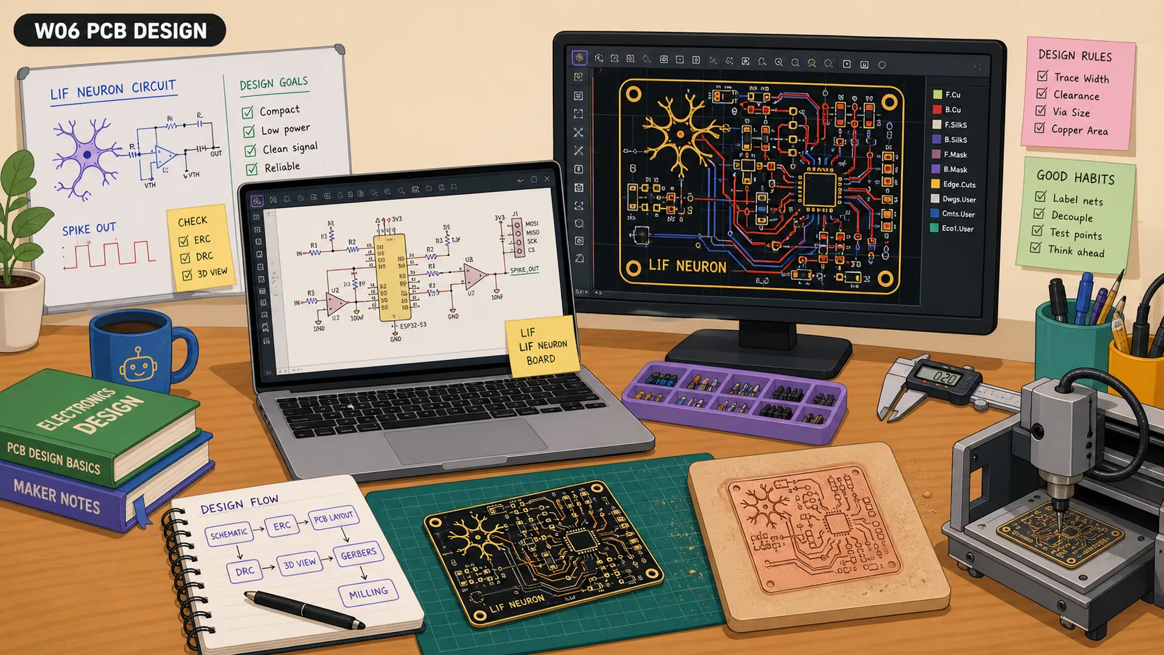
I designed my first PCB around a hardware LIF neuron idea, moving from circuit explanation to KiCad schematic, board layout, and manufacturing checks.
This week was my first ever experience with electronics design. Don't get me wrong, I was a straight A+ student in Physics class in high school, but going from theory to application is more difficult that it seems, especially if you're doing that while visiting a city you've dreamt of since you were a kid because you are a big Barcelona FC fan :)
Yup, during this week, I went to Barcelona for the MWC conference and got to work on the assignment at FabLab Barcelona, shoutout to their incredible team.
Group Assignment: Testing and Observing the Operation of a Microcontroller Circuit Board
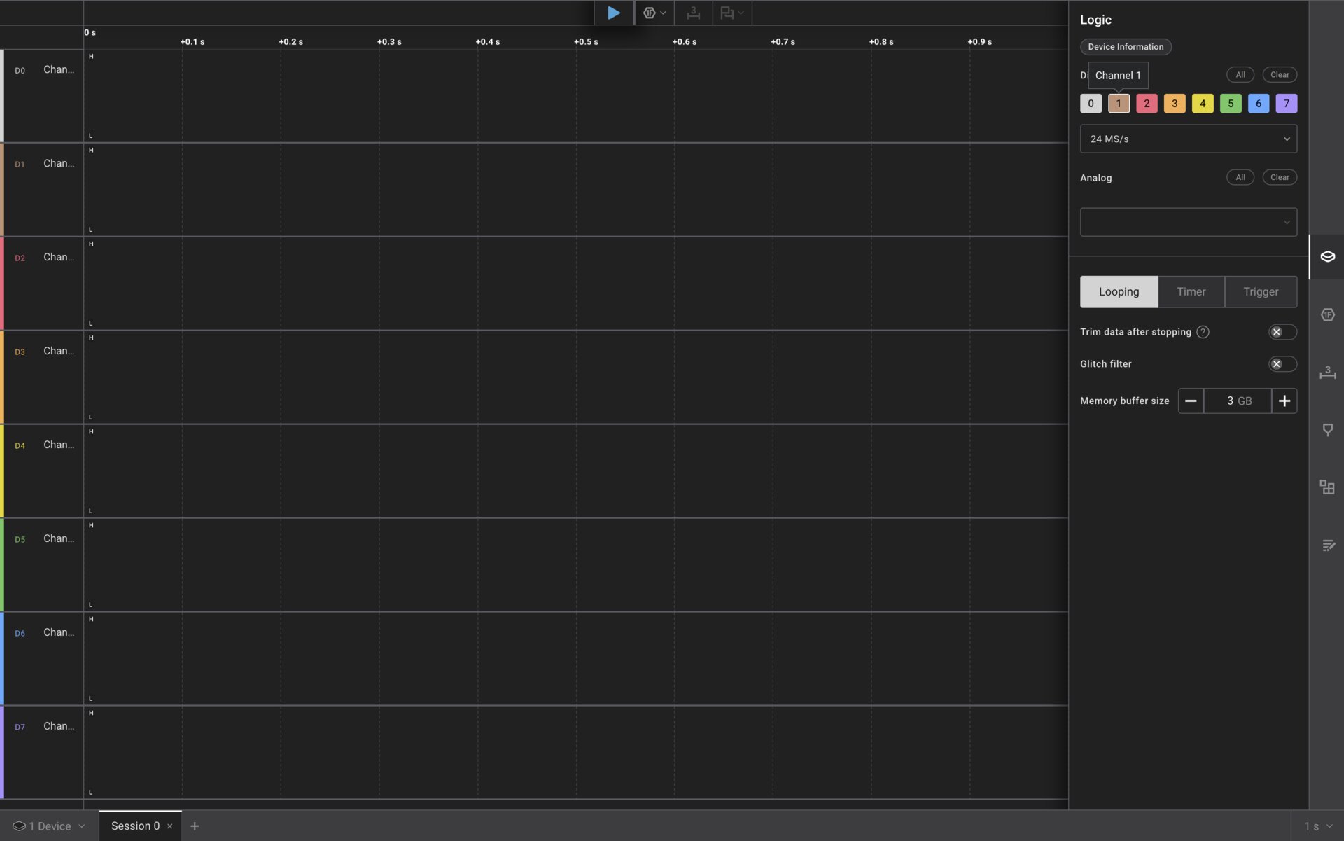
The group assignment this week was about testing how a microcontroller board behaves electrically. Not just "does the code run" but "what is the board actually doing with voltage over time." The full group write-up is linked above, but here are my personal reflections from the experience.
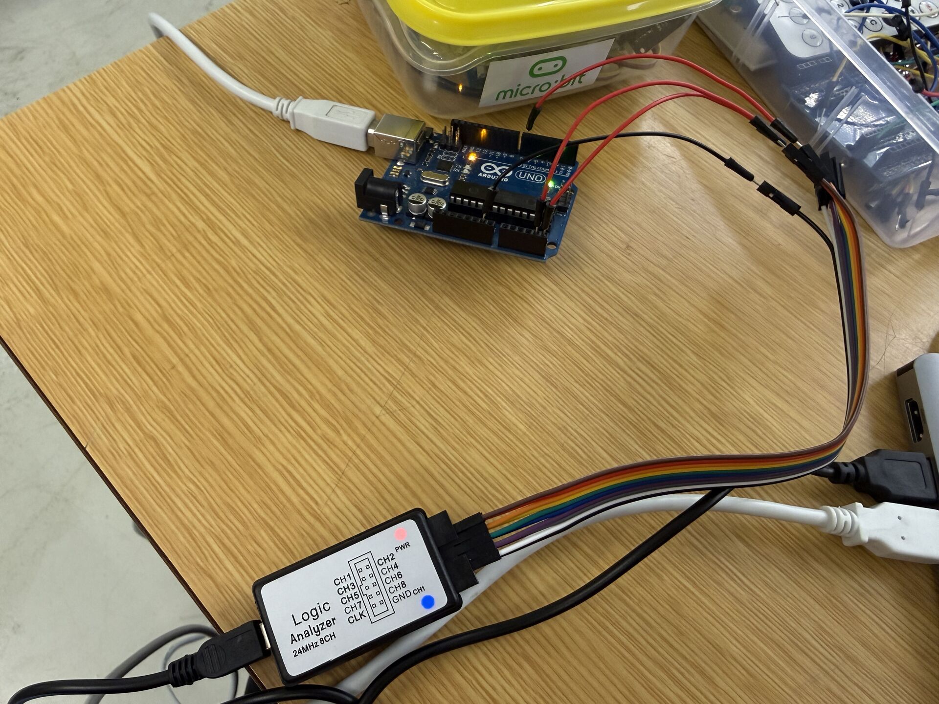
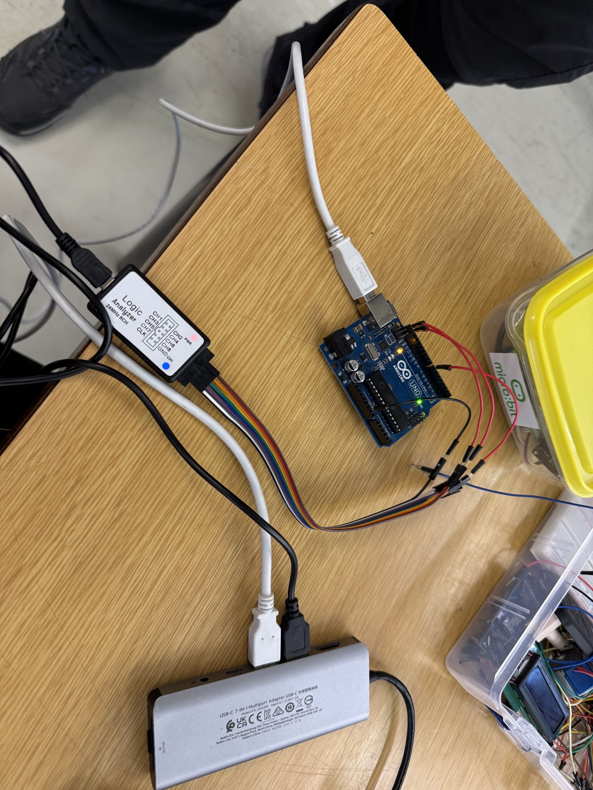
For me, this was the first time I touched a logic analyzer or an oscilloscope. I had used a multimeter before, sure, but actually seeing signals decoded on a screen in real-time was something else entirely.
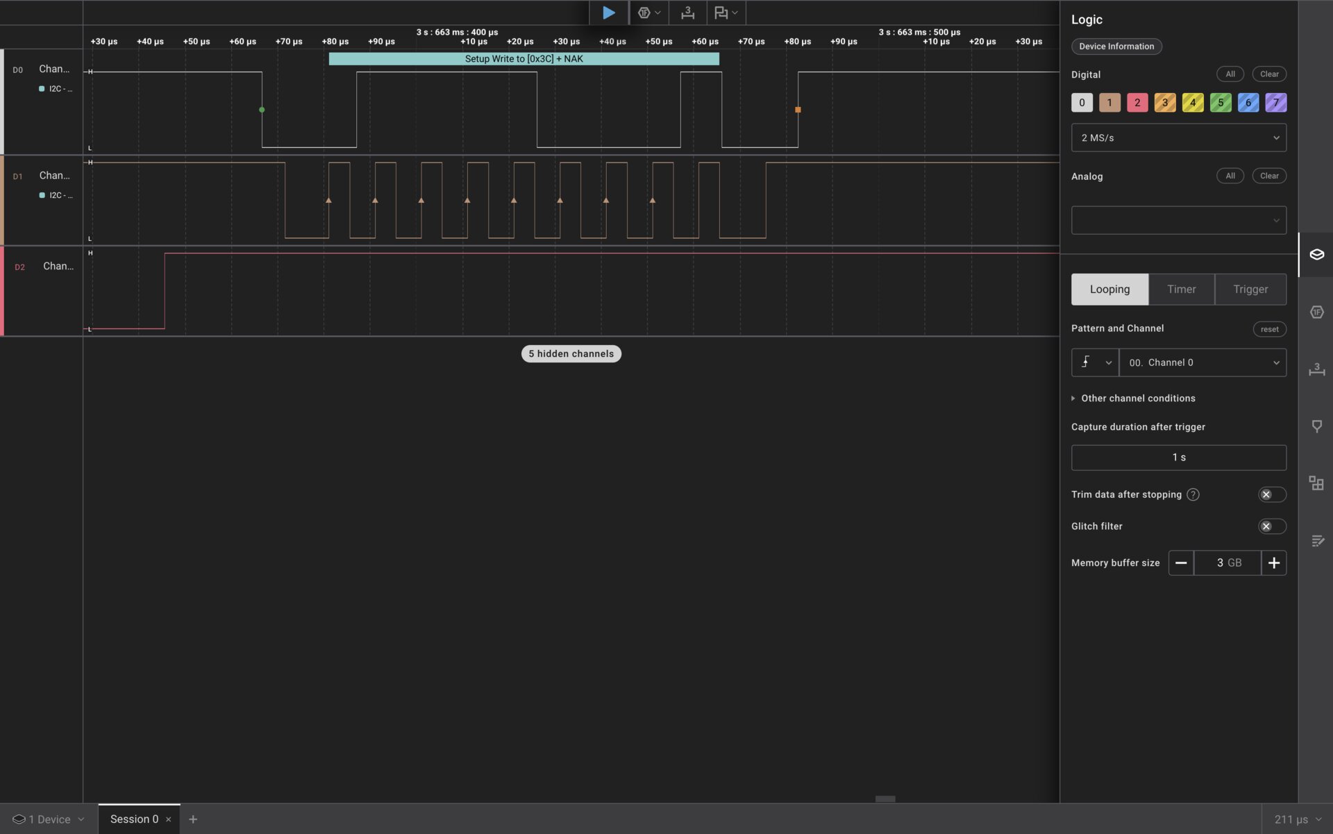
We ran two tests on an Arduino Uno. The first used a USB logic analyzer with Saleae's Logic 2 software to capture and decode I2C communication. We wrote a sketch that sends I2C transactions to address 0x3C every 500ms with no slave device attached.
When we hit capture, the logic analyzer showed us the START condition on the SDA line, the 7-bit address being clocked out bit by bit on SCL, and then the NACK that came back because nobody was listening on the bus.
That NACK (status code 2, ADDR_NACK) confused me for a moment until it clicked: of course no device is acknowledging, we intentionally had an empty bus. The microcontroller was doing its job, generating valid I2C traffic. The absence of an ACK was the bus telling us "nobody home."
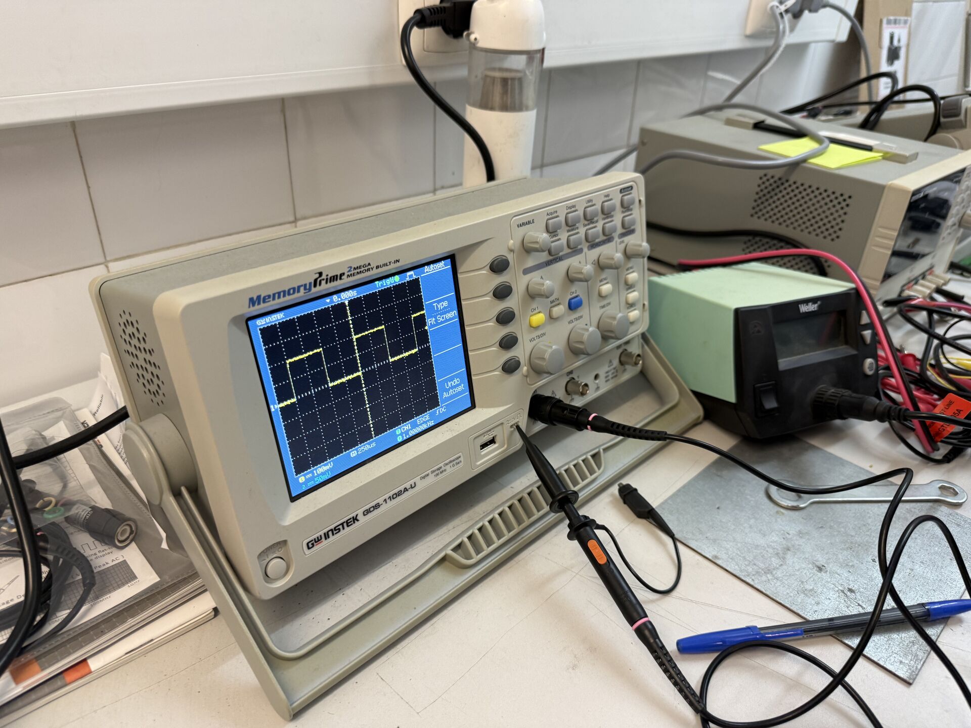
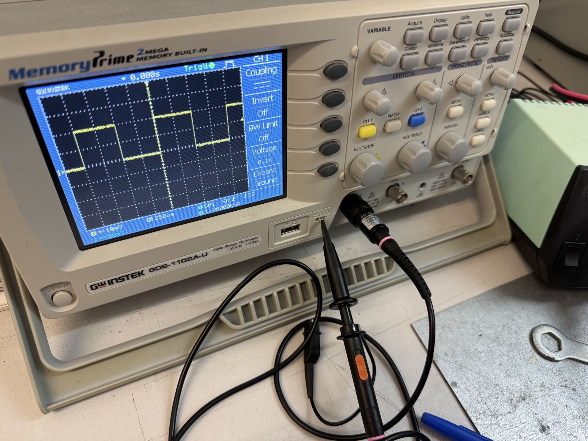
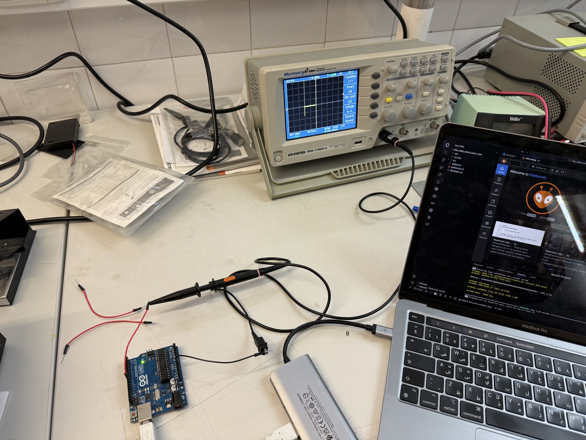
The second test used a GW Instek oscilloscope to look at PWM output on pin D9. The sketch ramped analogWrite from 0 to 255 in steps of 250ms, creating a gradual duty cycle sweep.
On the oscilloscope we could see the pulse width physically growing wider as the duty value increased, while the PWM frequency stayed locked at around 490 Hz. The full ramp cycle took about 64 seconds (256 steps x 250ms) before resetting back to zero.
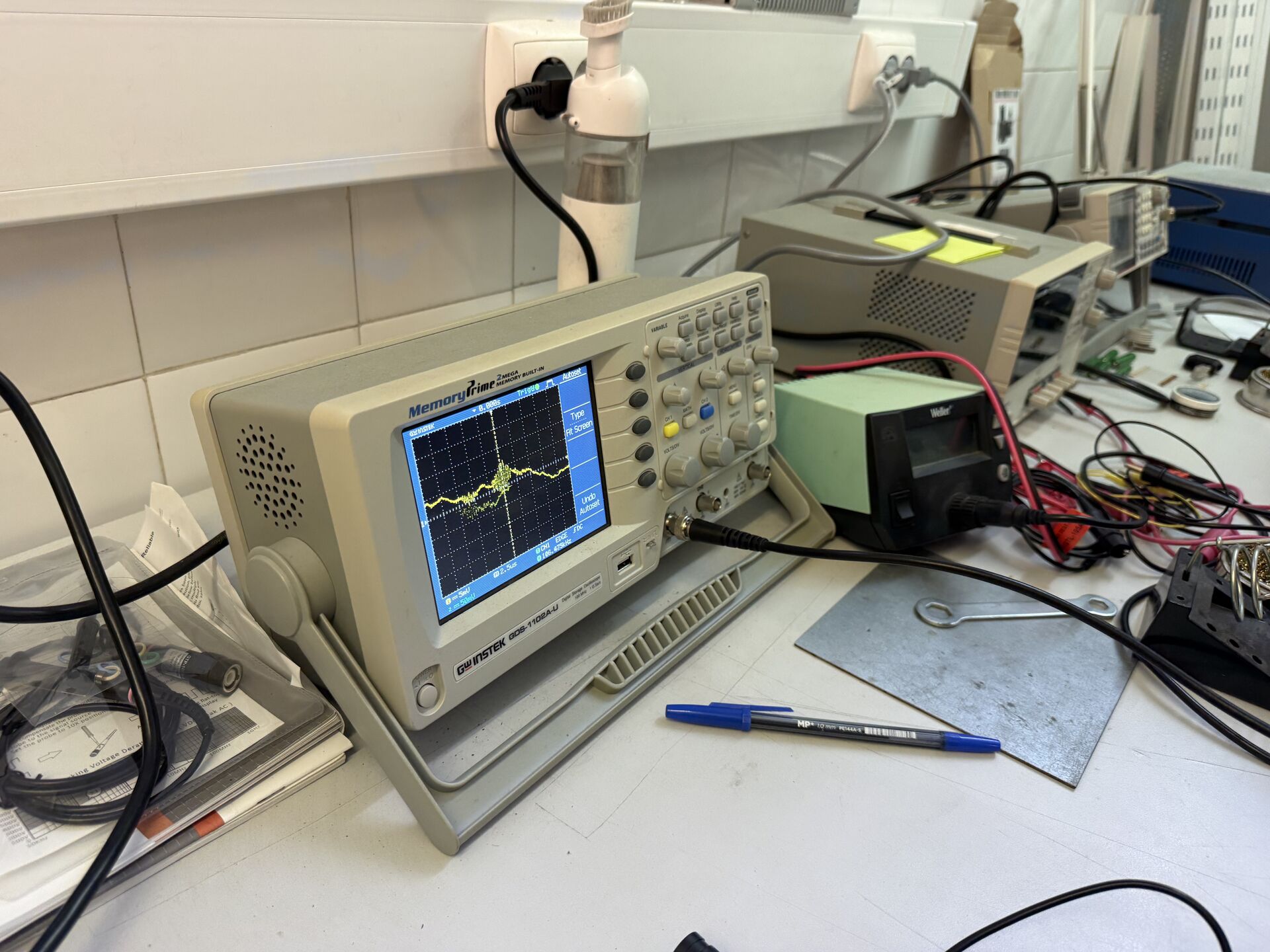
For fun, I also used the multimeter on the Arduino, and it worked as expected.
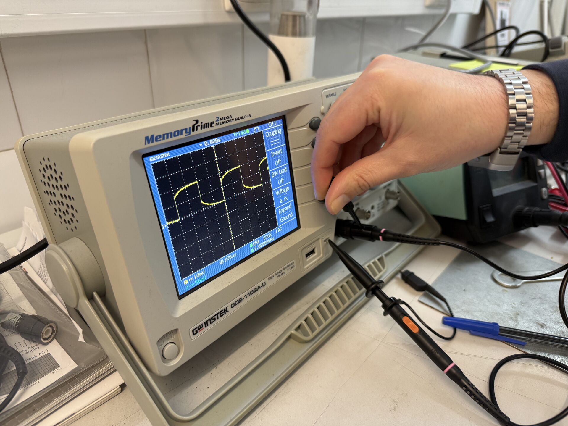
Also, I tried the same process but on my body… As you can see in the image below, it showed a positive number, but why?
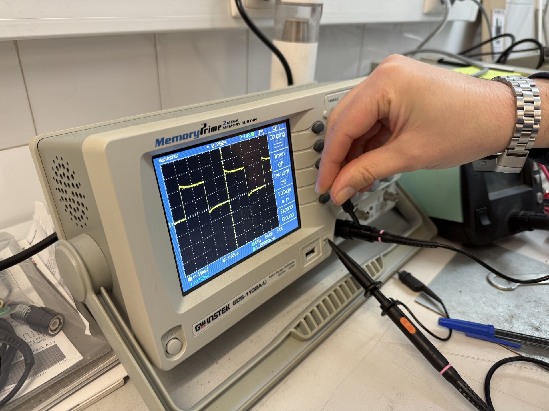
The wiring in the walls radiates a 50Hz electric field. My body, being mostly conductive saltwater with a large surface area, capacitively couples to that field and picks up a small induced voltage. When I hold both probes, I complete a circuit through my body and the multimeter measures that induced potential difference.
What I carried into the rest of the week from this group session was a feel for what "correct" signals look like. When I later started designing my own PCB with comparator outputs and analog signals, I already had a mental image of what those signals should look like on a scope or analyzer.
Learnings
Coming into this week, my knowledge of electronics was basically high school physics. I knew V = IR from class and I had used an Arduino before (and worked with some circuits during embedded programming week), but the gap between "knowing Ohm's law" and "designing a circuit board from scratch" turned out to be massive.
The global session this week, along with a lot of self-study outside of it, is where I started filling those gaps. I am writing this section specifically for people who, like me at the time, came into electronics design week with close to zero practical electronics knowledge.
Some of this came directly from the session, some from the Fab Academy class page, and some from my own research to understand things that were mentioned but not fully explained during the lecture.
Two books were recommended during the session: "The Physics of Information Technology" and "The Art of Electronics". I have not read them cover to cover, but read through them.
Passive Components
The first category of components we covered are called passive components because they do not amplify or generate signals. They just react to them.
A resistor limits current flow. The relationship is Ohm's law: V = I x R, where V is voltage in volts, I is current in amps, and R is resistance in ohms. If you have a 5V source and a 1000 ohm (1k) resistor, the current will be 5/1000 = 0.005 amps, or 5 milliamps.
Resistors come in different sizes and packages. In our lab we mostly use 0805 SMD (surface mount) resistors. One thing I learned is that the EU and US use different schematic symbols for resistors, so do not get confused if you see a zigzag line (US) versus a rectangle (EU) in different schematics.
A capacitor stores electrical charge. The amount of charge it can store per volt is its capacitance, measured in farads. The relationship is C = Q/V, and the current through a capacitor is related to the rate of change of voltage across it: I = C x dV/dt.
What this means practically is that capacitors block DC (steady voltage does not cause current to flow through them once charged) and allow AC (changing voltage does cause current flow).
Polarized capacitors (like electrolytic ones) can store more charge but they have to be connected the right way around or they can fail.
There are also supercapacitors which store orders of magnitude more charge (measured in farads rather than microfarads) and can even be used as small batteries.
In circuit designs, one of the most common uses for capacitors is as bypass or decoupling capacitors, where you place a small capacitor (typically 100nF) right next to an IC's power pin to filter out high-frequency noise and provide instant local charge when the IC needs a burst of current. Alongside these, bulk capacitors (typically 10µF–100µF electrolytics) sit on the power rail to handle larger, slower current demands — like when a motor starts up and briefly draws a spike of current the power supply can't respond to fast enough.
An inductor is in some ways the opposite of a capacitor. While a capacitor resists changes in voltage, an inductor resists changes in current. The voltage across an inductor is V = L x dI/dt. Inductors are useful for filtering and are often found in power supply circuits.
A common use case is placing a capacitor directly across a motor's terminals to absorb the voltage spikes generated by the motor's inductive coils when they switch. Without it, those spikes travel back down the power rail and can corrupt other parts of the circuit.
Crystals and resonators are components that vibrate at very precise frequencies. They are used to give microprocessors a stable clock signal. In some microcontrollers like the XIAO, the resonator is built into the chip itself, so you do not need an external one.
Semiconductors
Semiconductors are materials that conduct electricity under certain conditions but not others. This property is what makes modern electronics possible.
A diode allows current to flow in one direction only, from anode to cathode. An ideal diode would be a perfect one-way valve, but real diodes have a forward voltage drop (typically around 0.6V for silicon diodes, or 0.2V for Schottky diodes).
Below that forward voltage, the diode does not conduct. This is visible on the I-V curve of a diode, which shows essentially zero current below the threshold and then a rapid rise once the forward voltage is exceeded.
One interesting note from the session: the part of the diode curve where light is absorbed and converted to current is essentially how solar cells generate energy. Diodes are used in circuits to protect against reverse current, to rectify AC into DC, and in many other applications.
LEDs (Light Emitting Diodes) are diodes that emit light when current flows through them. Their I-V curve looks like a regular diode curve. One critical thing I learned this week: LEDs essentially ask for infinite current from whatever is driving them.
Without a current-limiting resistor in series, an LED will either destroy itself or fry the microcontroller pin driving it. So you always put a resistor before an LED.
To pick the right resistor value, you use Ohm's law: R = (Vsource - Vled) / Iled. For a typical LED with a 2V forward drop running at 10mA from a 5V source: R = (5 - 2) / 0.01 = 300 ohms, so you would use a 330 ohm resistor (the nearest standard value). DigiKey was recommended as the go-to source for checking component specs and datasheets.
Transistors
Transistors are where things get really interesting. There are two main families we care about: bipolar transistors (BJTs) and MOSFETs.
Bipolar transistors use a small current at the base pin to control a larger current flowing between collector and emitter. They always draw some current to operate, which makes them less power-efficient. We generally do not use them in our FabLab designs for that reason.
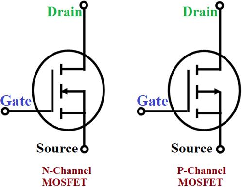
MOSFETs (Metal-Oxide-Semiconductor Field-Effect Transistors) use a voltage at the gate pin to control current flow between source and drain. Because the gate is insulated by an oxide layer, they draw almost zero current to switch, which makes them much more efficient.
There are two types: N-channel and P-channel. In an N-channel MOSFET, the source connects to ground and it sinks current (current flows into the drain). In a P-channel MOSFET, the source connects to the positive supply and it sources current (current flows out). For a motor that needs to spin in both directions, you need both types in an arrangement called an H-bridge.
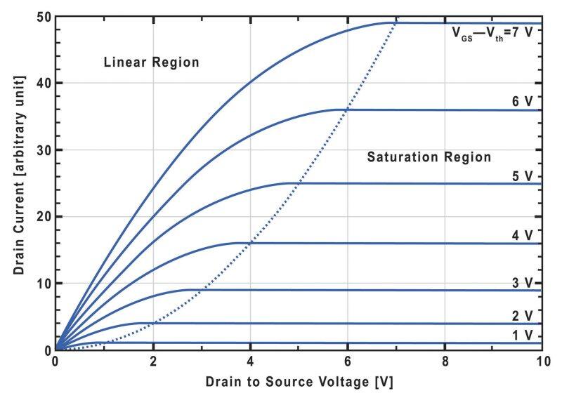
One important parameter for MOSFETs is Rds(on), which is the resistance between drain and source when the transistor is fully turned on. You want this to be as small as possible so the transistor does not waste power as heat. This directly affects how hot the transistor gets and how long your battery lasts.
On the I-V curve for a MOSFET, the slope in the linear region represents this resistance. A perfect conductor would be a vertical line, a perfect insulator would be horizontal, and a resistor is a straight line in between.
Power, Voltage Regulation, and Op-Amps
Every circuit needs a stable power supply. Voltage regulators take a varying input voltage and produce a consistent output. There are linear regulators (simpler, less efficient, waste energy as heat) and switching regulators (more complex, more efficient). Buck converters step voltage down and boost converters step voltage up.
An important detail: there is always an output capacitor near a voltage regulator to store charge and smooth out the output.
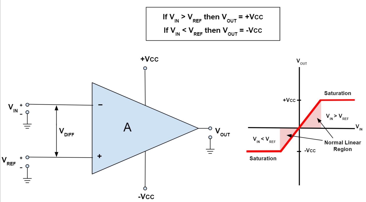
Op-amps (operational amplifiers) were also covered. They have extremely high gain and are used for signal amplification, buffering, filtering, and many other applications.
The I-V graph of an op-amp shows this huge gain characteristic. Our microcontrollers have built-in amplifiers (ADCs with adjustable gain), but for analog circuit design like the one I ended up doing this week, dedicated op-amps like the MCP6004 are what you want.
Circuit Fundamentals
A few basic rules that everything else in electronics builds on:
Everything in a circuit needs a path to ground. Ground (GND) is the reference point, the zero-volt baseline that all other voltages are measured against. Voltage supply rails are labeled VCC or VDD (positive).
Kirchhoff's Voltage Law (KVL) says that all the voltages around any closed loop in a circuit must add up to zero. Kirchhoff's Current Law (KCL) says that all the current entering a node must equal all the current leaving it.
These two rules, combined with Ohm's law, are the foundation for analyzing any circuit. Power dissipation also matters: P = I x V = I^2 x R. If a component is dissipating too much power, it gets hot and can fail.

EDA Tools and the Design Workflow
EDA (Electronic Design Automation) is the software used for designing circuit boards. The workflow goes like this: you start with a paper sketch, then enter the schematic in the EDA tool, place components, route traces, optionally simulate, and then fabricate.
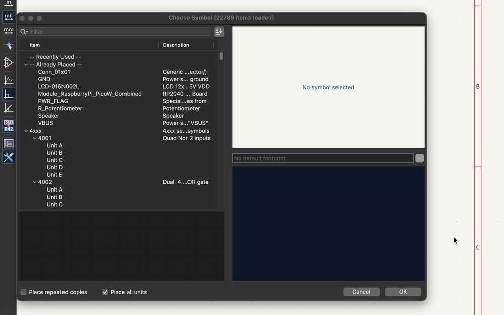
The session strongly recommended KiCad, which is open-source and loosely affiliated with CERN. It started as 6 separate programs that eventually came together into one suite. The key parts are the Schematic Editor (where you draw the logical circuit with symbols and connections) and the PCB Editor (where you lay out the physical board with real component footprints and copper traces).
A crucial concept is symbol libraries. Every component in your schematic needs a symbol (the logical representation showing what pins it has) and a footprint (the physical package showing what the pads look like on the board).
You need to assign the correct footprint to each symbol based on what packages you actually have in your lab's inventory. Kris from the Fab community created a KiCad library specifically for components available in a standard FabLab, available on the Fab Cloud GitLab.
The library is installed as a plugin. Download it from GitLab, then add it in KiCad under Preferences > Manage Symbol Libraries and Preferences > Manage Footprint Libraries. A big advantage of using it is that symbols already come with the correct footprints pre-assigned, so you don't have to manually map them later.
The full setup walkthrough is in the Fab Academy KiCad tutorial.
 Image from Fab Academy KiCad tutorial
Other EDA tools mentioned include Eagle (now part of Autodesk Fusion 360), Altium, and for simulation: Wokwi (great for digital simulation but does not enforce current limiting so be careful), Falstad (good for analog), and KiCad's built-in SPICE export. There are also hardware description languages like Verilog for describing circuits with billions of transistors programmatically, though that is more advanced than where we are right now.
For PCB design specifically, there are important design rules. You need to consider how many layers your board has, avoid sharp corners on traces (they etch differently and can cause signal integrity issues), understand vias (connections between top and bottom copper layers), and respect minimum trace widths and clearances for your specific fabrication process.
The DRC (Design Rule Check) in KiCad verifies that your board satisfies all these constraints before you send it to fabrication. The ERC (Electrical Rules Check) verifies that your schematic is logically correct, things like unconnected pins, shorted power nets, and missing power flags.
Test Equipment
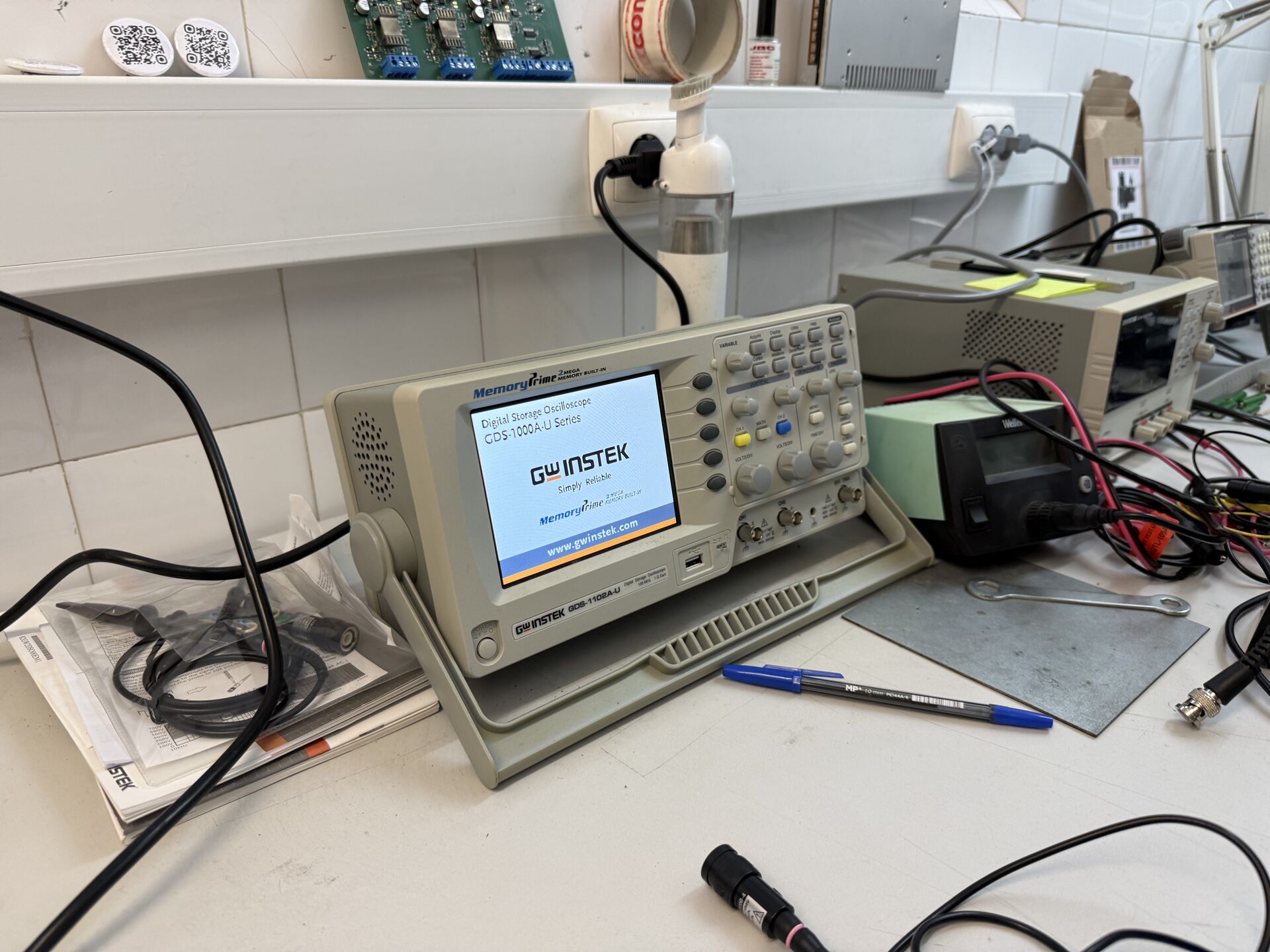
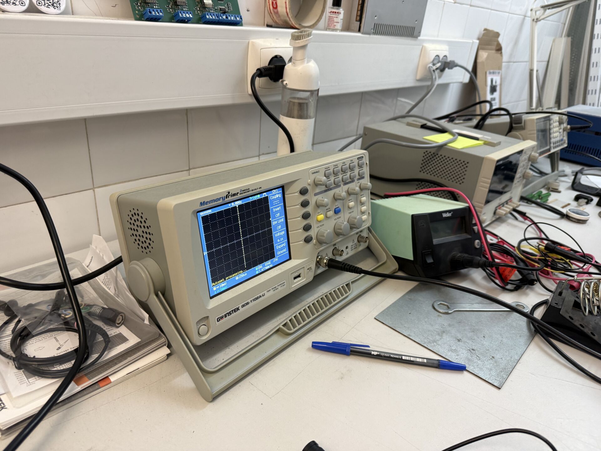
Test equipment is not optional, it is essential for debugging. Multimeters measure voltage, current, and resistance. Oscilloscopes show you voltage over time as a waveform, useful for both analog and digital debugging. Logic analyzers connect to multiple signal lines and decode digital protocols like I2C, SPI, and UART.
Designing My Own PCB
Explanation of My Circuit Idea: LIF Neuron Model
This week I wanted to design something I had in mind from the start of the program: a circuit that mimics how the brain. Not a simulation running on a computer, but real analog hardware where real charge accumulates on a real capacitor and a real comparator decides when to fire a spike.
To understand what I am building, it helps to understand what I am trying to model. So let me walk through the biology first, then the math, and then how it all translates to actual circuit components.
I did a version of this explanation during the computer-controlled cutting week, but I think it is worth reiterating since we need to get to a bit more details here.
The Biological Neuron
Before building the circuit, it's worth understanding what we're mimicking. A biological neuron is the fundamental computational unit of the nervous system. The human brain contains roughly 86 billion neurons, each connected to thousands of others.
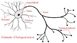
Dendrites: tree-like branches that receive incoming signals (electrical or chemical) from neighboring neurons
Soma (cell body): integrates all incoming signals over time
Axon hillock (the decision point): if total accumulated input crosses a threshold, the neuron fires
Axon: transmits the electrical spike (action potential) downstream
Synaptic terminals: release neurotransmitters across the synapse to the next neuron's dendrites
The Membrane Potential
A neuron's membrane separates the intracellular fluid (rich in K⁺) from the extracellular fluid (rich in Na⁺). This ionic imbalance creates a resting membrane potential of about −70 mV.
When the neuron receives input, ion channels open and Na⁺ rushes in, raising the membrane voltage. If that voltage climbs past the threshold (~−55 mV), a rapid, self-amplifying cascade occurs — the action potential:
- Voltage rises explosively to ~+40 mV (depolarization)
- K⁺ channels open, voltage drops back below rest (repolarization + hyperpolarization)
- The neuron enters a brief refractory period (~2 ms) where it cannot fire again
- Ion pumps restore the resting state

The total spike lasts ~1–2 ms and propagates down the axon as a stereotyped pulse. Its amplitude doesn't vary, only its timing and frequency carry information.
The LIF Model
The Leaky Integrate-and-Fire (LIF) model was first proposed by Louis Lapicque in 1907, and it remains one of the most widely used neuron models in computational neuroscience today. Even though it isn't biologically accurate it is computationally very efficient.
Forget ion channels, neurotransmitters, and dendritic morphology. It keeps only three behaviors:
| Behavior | What the Biology Does |
|---|---|
| Integrate | Soma sums incoming currents, raising membrane voltage |
| Leak | Ion channels passively drain charge, pulling V back to rest |
| Fire | All-or-nothing spike when V crosses threshold |
| Reset | Refractory period, voltage snaps back to resting |
The Math
The LIF model is governed by a single first-order differential equation. Here it is, and below it, every symbol mapped to our actual circuit:
The core LIF equation:
τm · dV/dt = −(V − Vrest) + Rm · I(t)
Breaking it down:
τm · dV/dt : rate of change of membrane voltage, scaled by the time constant
−(V − Vrest) : the leak term: pulls V back toward resting potential
Rm · I(t) : the input term: current from synapses (or our potentiometer) drives V up
Variables mapped to our circuit:
| Symbol | Meaning | Our Circuit Value |
|---|---|---|
| V(t) | Membrane voltage at time t | Voltage at V_mem node |
| Vrest | Resting potential | V_GND = 2.5 V |
| τm = Rm × Cm | Membrane time constant | 100 kΩ × 22 µF = 2.2 s |
| Rm | Membrane resistance | R_leak = 100 kΩ |
| I(t) | Input current | Controlled by 10 kΩ potentiometer |
| Vthresh | Firing threshold | 3.65 V (set by R5=10k, R6=27k voltage divider on LM339) |
| Vreset | Post-spike reset voltage | V_GND = 2.5 V (via BSS84 MOSFET) |
The firing rule:
if V(t) ≥ Vthresh → fire spike! → V resets to Vreset (= Vrest)
Analytical solution: how V(t) evolves in time with no firing, constant input I:
V(t) = Vrest + Rm·I · (1 − e^(−t/τm)) + (V₀ − Vrest) · e^(−t/τm)
This is simply an exponential charge-up toward steady-state Vrest + Rm·I. Two cases:
If Vrest + Rm·I < Vthresh → V saturates below threshold → neuron never fires
If Vrest + Rm·I ≥ Vthresh → V will eventually cross threshold → neuron fires repeatedly
Inter-spike interval (time between consecutive spikes under constant input I):
T_ISI = τm · ln[ (Rm·I + Vrest − Vreset) / (Rm·I + Vrest − Vthresh) ]
And the firing rate: f = 1 / T_ISI
Higher input current → shorter T_ISI → faster firing rate. This is the neuron's rate coding mechanism — the same information encoding strategy used by your real neurons right now.
Why Does This Map Well to an RC Circuit?
The LIF equation is mathematically identical to the standard RC circuit voltage equation:
RC · dV/dt = −(V − Vin)
This is not a coincidence. Lapicque derived the LIF model from the RC analogy. The cell membrane is literally a leaky capacitor:
| Biological Component | Circuit Equivalent |
|---|---|
| Lipid bilayer | Capacitor: separates charge across the membrane |
| Ion channels (K⁺, Na⁺ leak) | Resistor: conducts current, sets the leak rate |
| Synaptic input currents | Current source: drives the membrane voltage up |
| Na⁺/K⁺ pump | Voltage reference: maintains the resting "battery" offset |
| Axon hillock threshold | Comparator: fires when voltage crosses a set point |
| Refractory period | RC timer + reset switch: forces a fixed dead time |
By building this circuit, we're not just simulating a neuron in software. We're implementing the exact physical analog that Lapicque had in mind, with real charge accumulating on a real capacitor, and a real threshold comparator deciding when to fire.
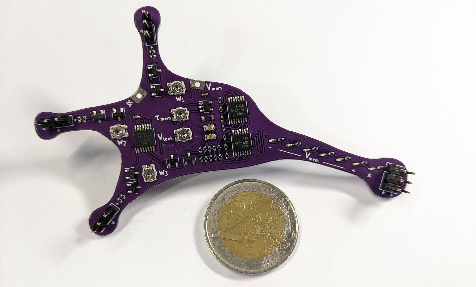
Now for how I actually turned this into a real circuit. My design is based on the lu.i neuron PCB project (github.com/giant-axon/lu.i-neuron-pcb), which is an open-source analog neuron design. Credit goes to the lu.i team for the original circuit architecture.
However, lu.i was designed to run on a 3V CR2032 coin cell with a charge pump to generate a negative rail. That is not practical for what I needed, so I adapted the design to run on 5V USB power with a virtual ground at 2.5V. I also simplified it down to a single synapse input (lu.i has three) since I wanted to focus on understanding one neuron clearly before scaling up.
From lu.i I kept the MCP6004 quad rail-to-rail op-amp (works across the full 0-5V range unlike the LM358 which has a dead zone near VDD), the LM339 quad comparator (open-collector output is perfect for threshold detection), the BSS84 P-channel MOSFET for membrane reset (the active-LOW spike signal directly drives a PMOS gate without needing an inverter), and the comparator-based refractory timer (saves an entire NE555 IC by reusing one of the four comparators we already have in the LM339).
What I changed: the power supply (5V USB instead of 3V coin cell), the number of synapses (one potentiometer instead of three), the input type (DC from a pot instead of exponentially decaying current), and the membrane parameters (fixed at R_leak = 100k ohm, C_mem = 22uF instead of tunable via pots).
These simplifications make the circuit easier to understand while keeping the core neuroscience behavior intact.
One more addition that lu.i does not have: since this week's assignment required integrating a microcontroller, I added a Xiao ESP32-S3 to the board.
The whole board is powered through the Xiao's USB-C connector, which provides the 5V that feeds the entire analog neuron circuit. The Xiao reads the potentiometer position through an ADC pin (with a voltage divider to scale the 0-5V pot range down to the 0-3.3V range the Xiao can handle) and displays the input current value on a small I2C OLED screen.
So the analog neuron circuit does all the actual neuron behavior on its own with no code involved, and the Xiao just sits alongside it as a readout tool. The neuron fires without the MCU, the MCU just tells you what the input knob is set to.
KiCad Basic Interface
Once KiCad is open and you've created a project, you work in two main editors: the Schematic Editor for the logical circuit and the PCB Editor for the physical layout. Here's what the core actions look like in the Schematic Editor:
Adding symbols: Press A to open the symbol chooser. Search for the component you need (e.g. "R" for resistor, "C" for capacitor), select it and click to place it on the canvas. If you're using the Fab library, search within it to get components with pre-assigned footprints.
Drawing connections (wires): Press W to start a wire. Click to draw between component pins to connect them electrically. A green dot appears where wires join, confirming a proper connection.
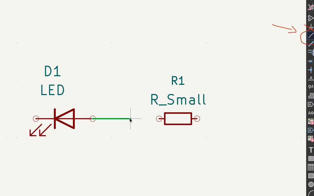
Net labels: Instead of drawing long wires across the schematic, you can place a net label (L) on a pin and give it a name. Any two pins sharing the same label name are electrically connected, even if there's no visible wire between them. This keeps the schematic readable.
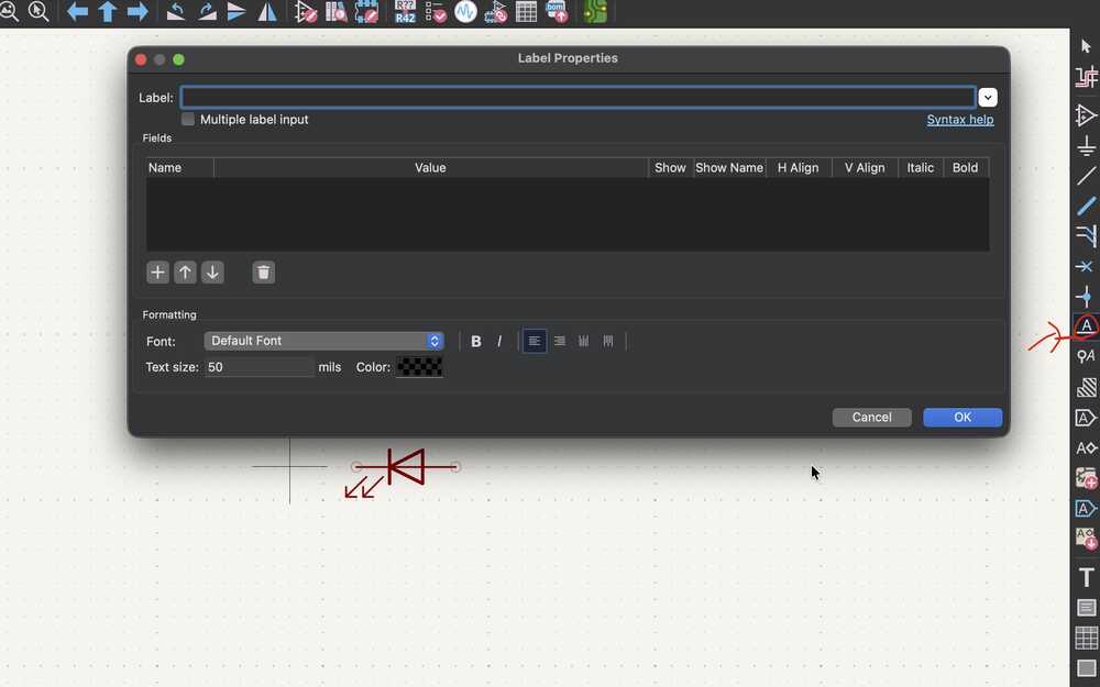
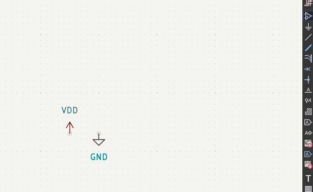
Power symbols: Press P to add power symbols like VDD, GND, or +3V3. These are special net labels that represent power rails. Every power net needs at least one PWR_FLAG to tell the ERC that the net is actually driven — without it you'll get errors.
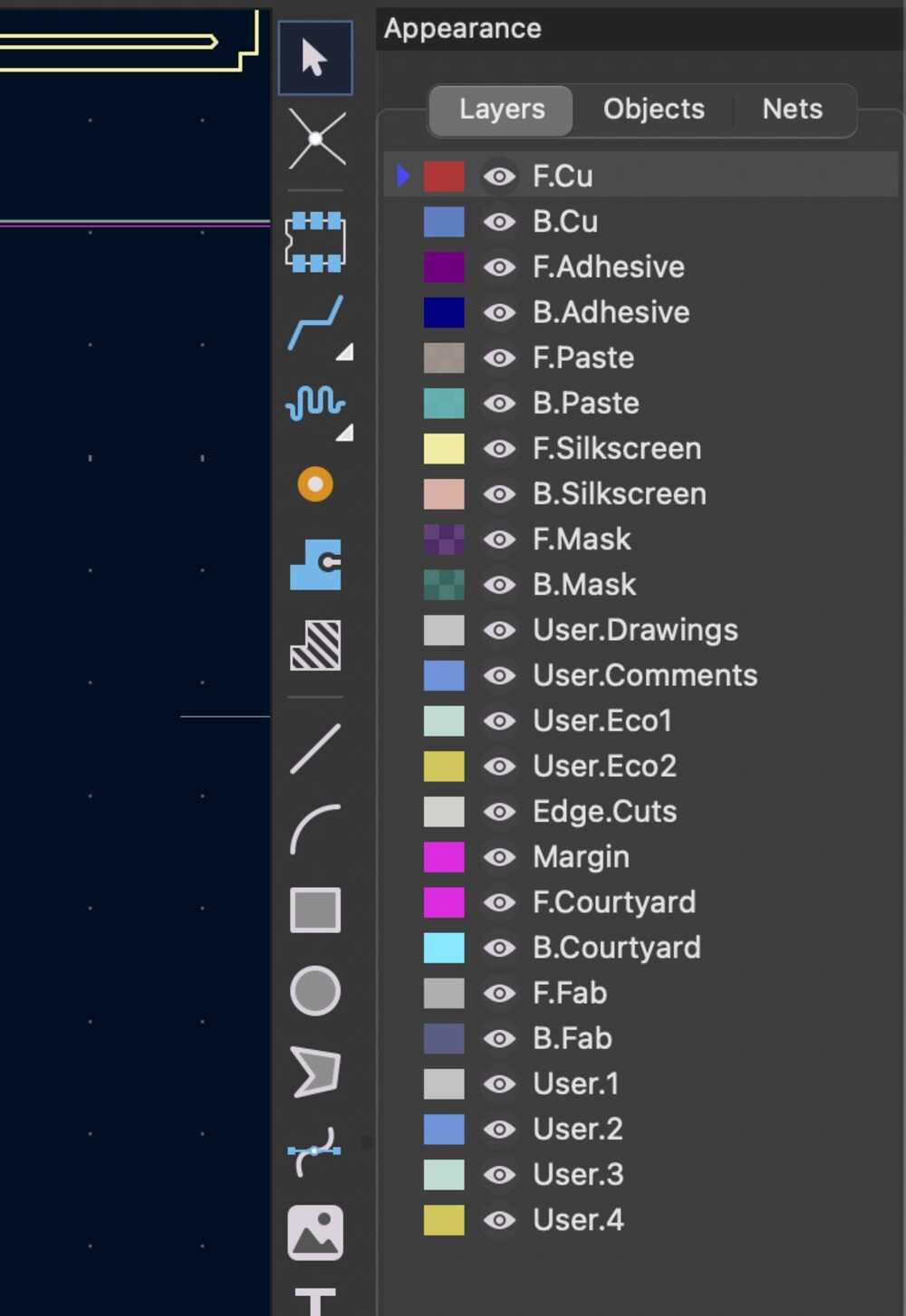
Layers: In the PCB Editor, each layer represents a different physical layer of the board. You select the active layer from the layers panel on the right. The key layers are:
F.Cu— front copper (top traces)B.Cu— back copper (bottom traces). A via connects the two.F.Silkscreen— front labels and reference designators, printed on the board surfaceF.Courtyard— the boundary around each component, used to detect overlapsEdge_Cuts— the board outline; whatever shape you draw here is where the mill cuts
To route a trace, select the copper layer you want, press X and click between pads. In a fablab setting you generally want to stick to one layer (F.Cu) as much as possible since double-sided boards are harder to mill and align.
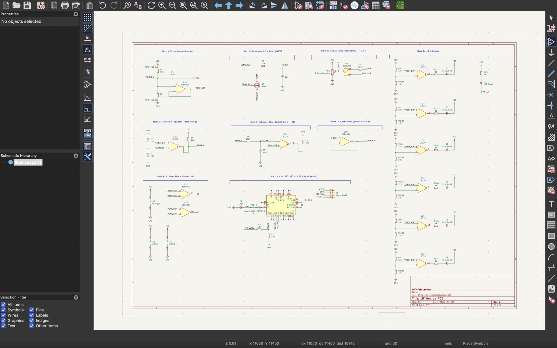
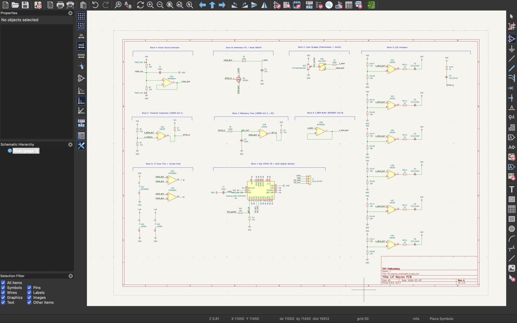
Schematic Design
I used KiCad 9 for the schematic. The circuit is organized into functional blocks, each one corresponding to a part of the neuron's behavior. I will walk through each block and explain what it does and how I built it in the schematic editor.
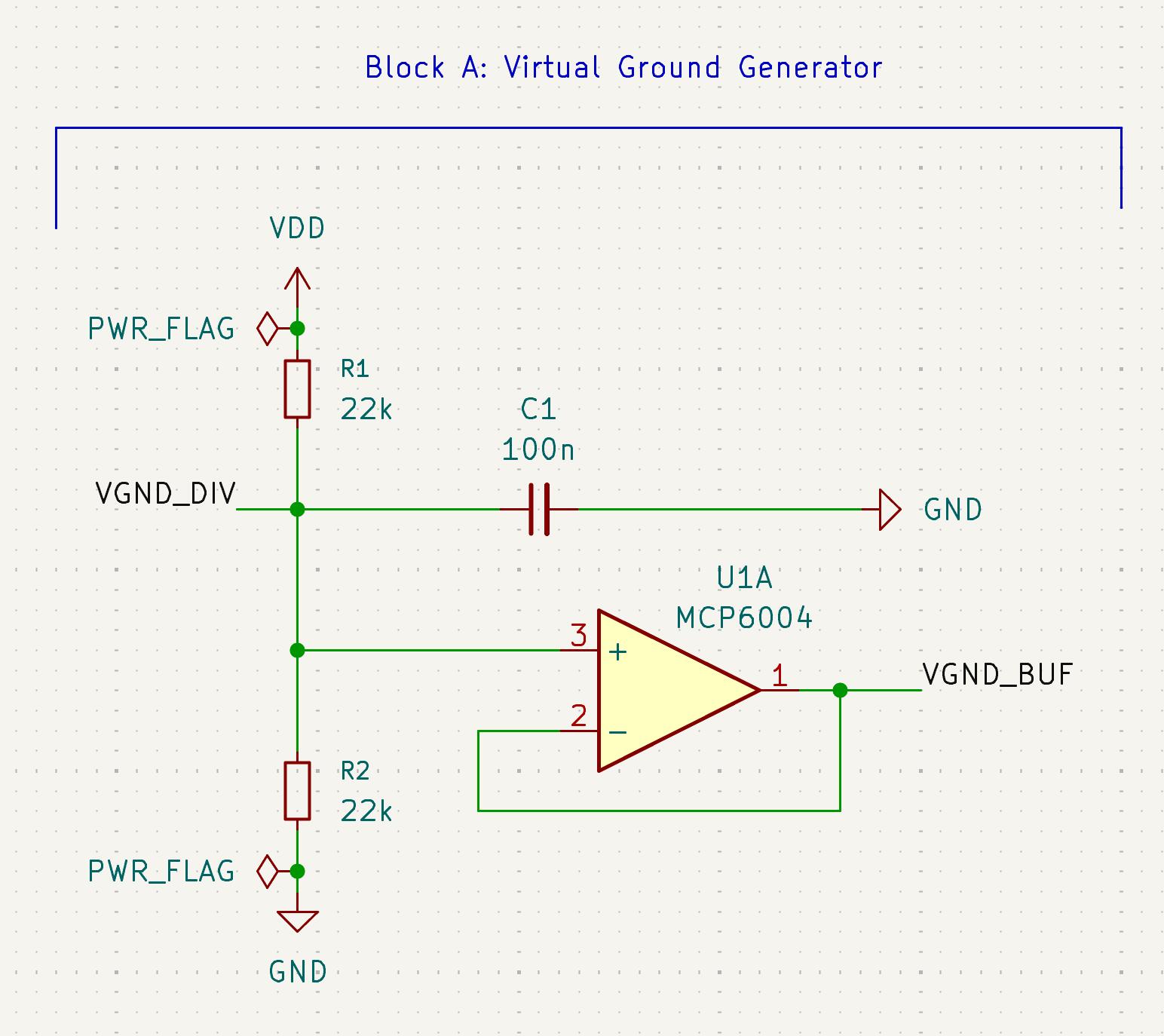
Block A: Virtual Ground Generator (VGND)
Since the circuit runs on 5V USB, I needed a stable 2.5V reference to act as the neuron's "resting membrane potential." This is created by a simple voltage divider (two 22k ohm resistors between VDD and GND) followed by an MCP6004 op-amp in voltage-follower configuration.
The voltage divider alone would have high impedance, meaning any load would pull the voltage down. The op-amp buffer has very high input impedance and very low output impedance, so it acts as a "stiff" 2.5V source that can supply current without sagging. I also placed a 100nF bypass capacitor on the divider midpoint to filter high-frequency noise.
Voltage calculation: V_VGND = 5V x 22k / (22k + 22k) = 2.5V
In KiCad, I placed two R_Small symbols vertically with VDD at the top and GND at the bottom, added a junction dot at the midpoint, placed the C_Small horizontally to the right going to GND, and then placed the MCP6004 Unit A with IN+ connected to the divider midpoint and OUT wired back to IN- for the feedback loop. The output gets the net label VGND_BUF.
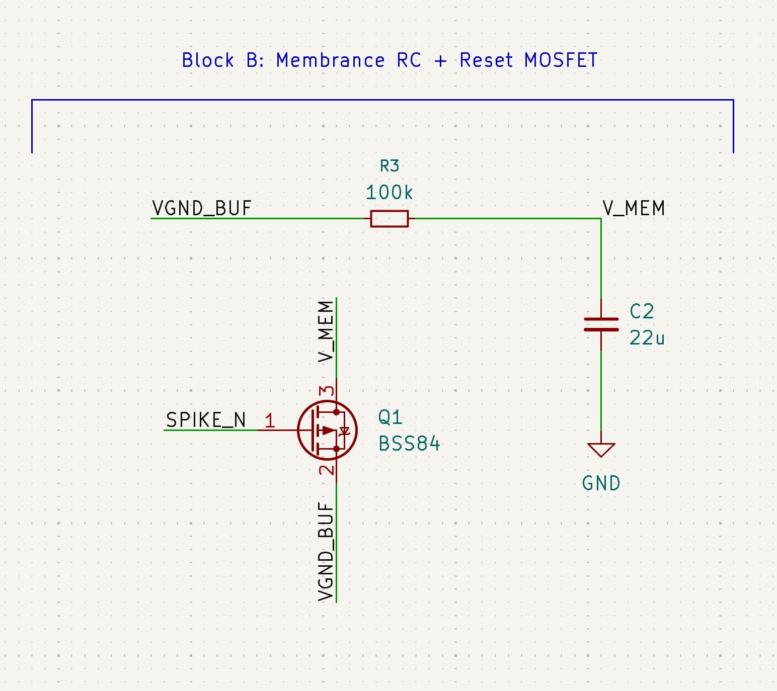
Block B: Membrane RC and Reset MOSFET
This is the actual "neuron membrane." A 100k ohm resistor (R_leak) connects VGND_BUF to the membrane node V_MEM, and a 22uF capacitor (C_mem) connects V_MEM to ground. This RC pair is the physical implementation of the LIF equation. The capacitor charges up when input current flows in, and the resistor constantly leaks charge back toward the 2.5V resting potential.
The time constant is tau = R_leak x C_mem = 100k x 22uF = 2.2 seconds. This means the membrane takes about 2.2 seconds to charge to 63% of its final value. I chose these values to make the charging visible to the human eye on the LEDs.
The BSS84 P-channel MOSFET handles the reset. When the neuron fires a spike, the SPIKE_N signal goes LOW (because the LM339 has an open-collector output that pulls to ground). This LOW signal on the BSS84's gate turns it ON (PMOS turns on when gate is below source), shorting V_MEM back down to VGND_BUF (2.5V). The gate-source voltage during a spike is 0V - 2.5V = -2.5V, which exceeds the BSS84's threshold of about -1.5V, so the MOSFET conducts.
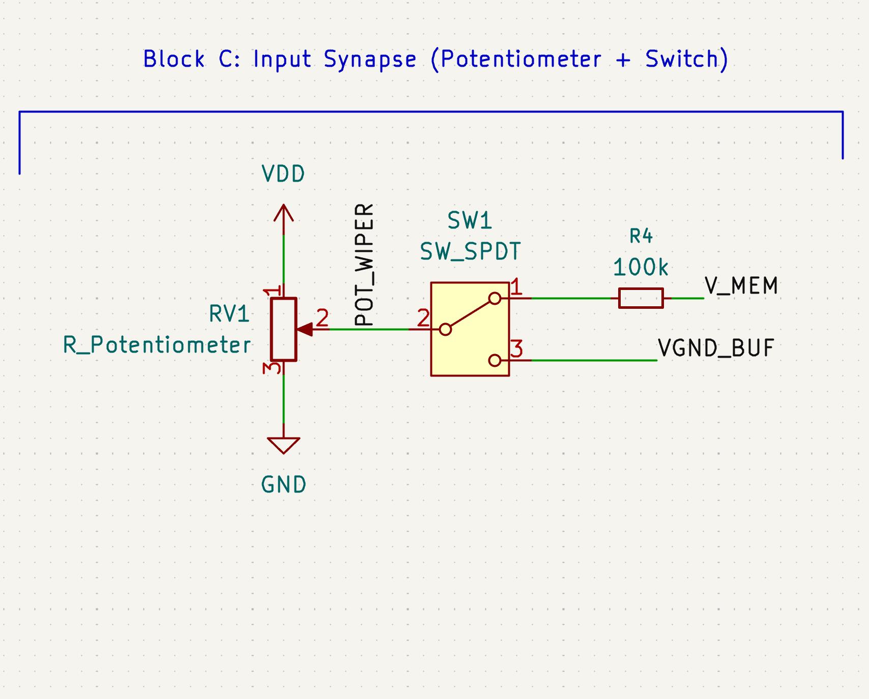
Block C: Input Synapse (Potentiometer and Switch)
The potentiometer (10k ohm) acts as the synaptic input. Its top terminal goes to VDD, bottom to GND, and the wiper goes through an SPDT switch and then a 100k ohm input resistor (R_in) to the V_MEM node. The switch lets you toggle between excitatory mode (pot wiper connected through R_in to the membrane, so current flows) and inhibitory mode (pot wiper connected to VGND_BUF, so there is no voltage difference and no current flows).
R_in being the same value as R_leak (both 100k) means input current and leak current have equal weight. When the pot is at max (5V) and the membrane is at rest (2.5V), the input current is (5 - 2.5) / 100k = 25 microamps. As the membrane charges toward threshold, the leak current increases and the input current decreases, creating the natural balance that determines the firing rate.
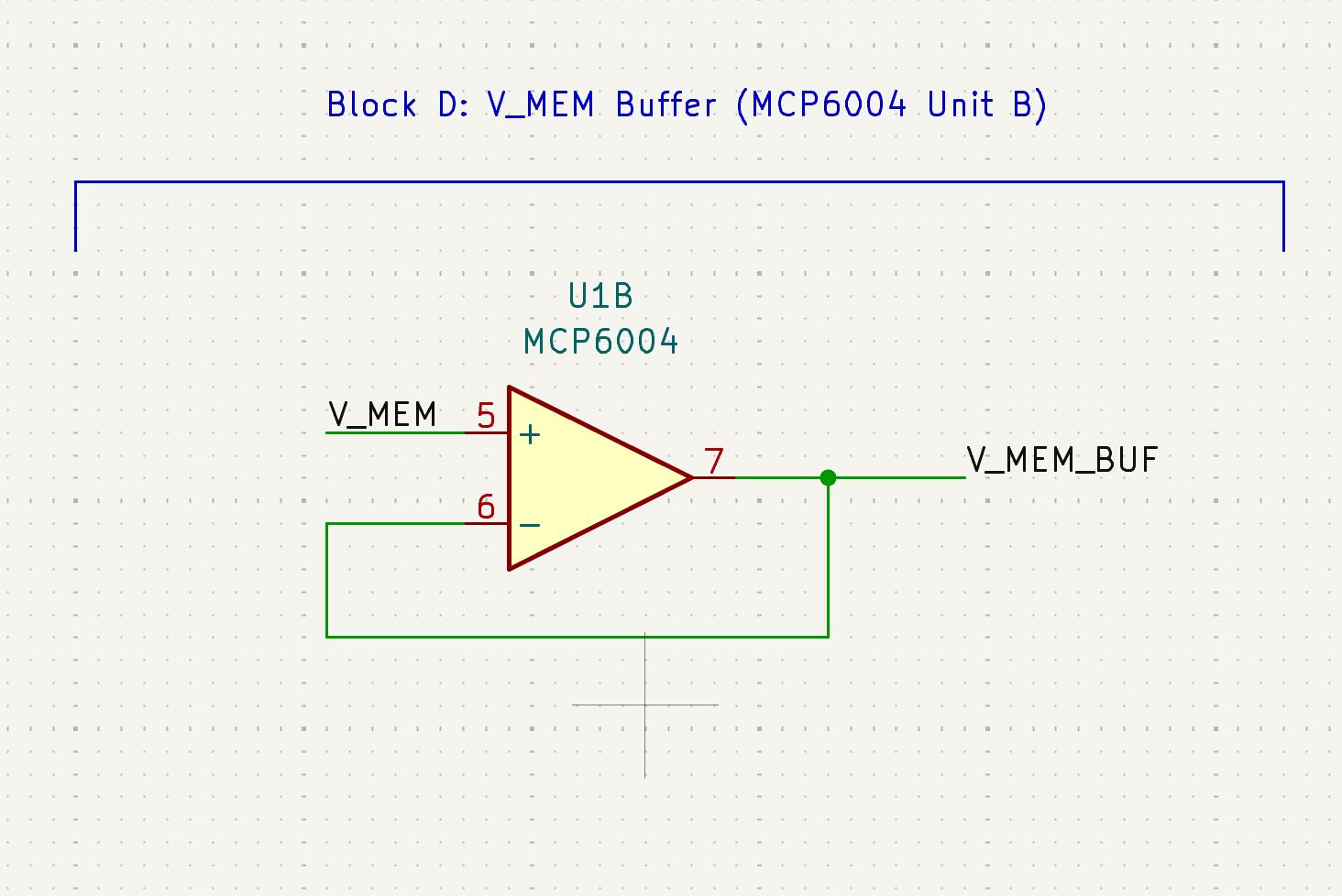
Block D: Membrane Voltage Buffer
Another MCP6004 unit (Unit B) configured as a voltage follower, this time buffering V_MEM. Without this buffer, the comparators downstream would load the delicate RC membrane and disturb its charging behavior. The buffer provides V_MEM_BUF as a copy of the membrane voltage that can safely drive multiple comparator inputs. Same wiring as Block A: IN+ gets V_MEM, OUT goes back to IN-, and the output gets labeled V_MEM_BUF.
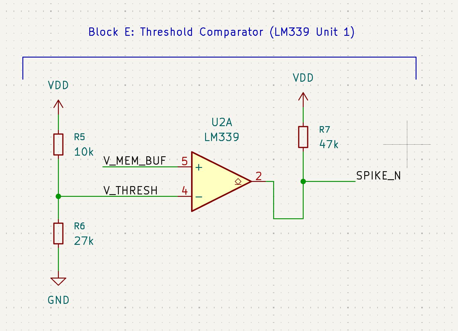
Block E: Threshold Comparator
The LM339 Unit 1 compares V_MEM_BUF (on IN+) against a fixed threshold voltage V_THRESH (on IN-). The threshold is set by another voltage divider: R5 (10k) and R6 (27k) between VDD and GND, giving V_THRESH = 5V x 27k / (10k + 27k) = 3.65V.
The LM339 has an open-collector output. When V_MEM_BUF is below threshold, the output floats and a 47k pull-up resistor holds SPIKE_N at VDD (HIGH = no spike). When V_MEM_BUF exceeds threshold, the output transistor turns ON and pulls SPIKE_N to ground (LOW = spike firing). This active-LOW signal directly drives the BSS84 PMOS gate in Block B.
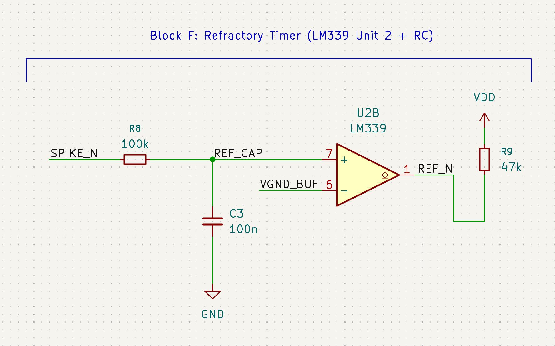
Block F: Refractory Timer
After a spike fires, the neuron needs a brief refractory period where it cannot fire again, otherwise the comparator would oscillate continuously while V_MEM is being reset. The refractory timer uses LM339 Unit 2 plus an RC network (100k and 100nF, giving tau = 10ms). When SPIKE_N goes LOW during a spike, current flows through the RC, and the comparator holds the system in the fired state until the capacitor charges past VGND_BUF. After about 10ms, the refractory period ends and the neuron is ready to fire again.
This approach was borrowed from lu.i and is more elegant than using a separate NE555 timer IC, since we already have four comparators in the LM339 package.
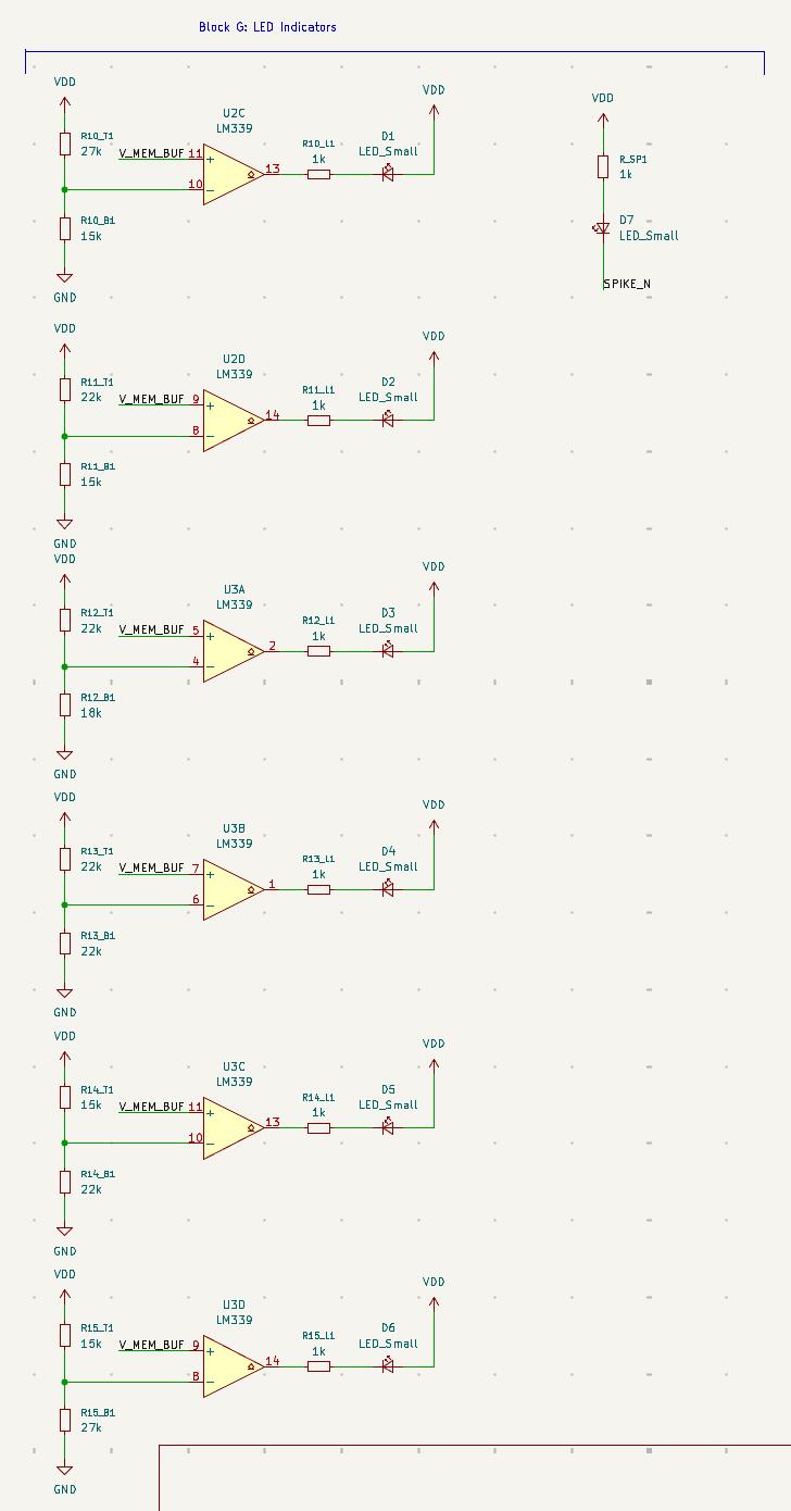
Block G: LED Display
The LED display shows the membrane voltage level using multiple LEDs. Each LED is driven by a separate LM339 comparator unit that compares V_MEM_BUF against a different threshold voltage set by its own resistor divider. As the membrane charges up, the LEDs light up one by one from low to high, creating a visual representation of the membrane potential climbing toward threshold. When the neuron fires, a separate spike LED lights up.
Each LED has a 1k current-limiting resistor in series. The comparator's open-collector output sinks current through the LED when the membrane voltage exceeds that LED's threshold.
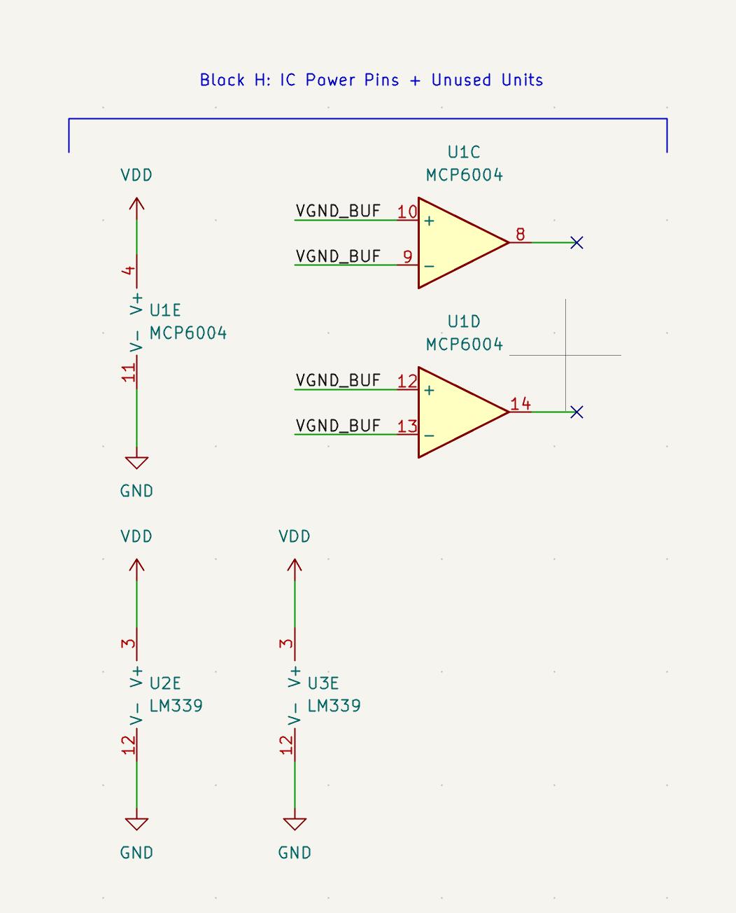
Block H: Power Pins and Unused Units
Both the MCP6004 and LM339 are multi-unit ICs. The MCP6004 has 4 op-amp units plus a power unit, and the LM339 has 4 comparator units plus a power unit. KiCad requires every unit to be placed in the schematic. For unused op-amp units (C and D of the MCP6004), I tied both inputs to VGND_BUF and placed no-connect markers on the outputs. The power units for both ICs get VDD and GND connections.
Block I: Xiao ESP32-S3 and OLED (Digital Section)
This block is the MCU integration I mentioned earlier. The Xiao ESP32-S3 sits on the board and its 5V pin (pin 14) provides VDD for the entire analog neuron circuit, so when you plug in a USB-C cable the whole board powers up. On the input side, I needed to read the potentiometer wiper voltage so the OLED can display what the input current is set to. The problem is the pot wiper ranges from 0 to 5V but the ESP32-S3 ADC can only handle up to 3.3V. Feeding 5V directly into the ADC pin would damage it. So I added a voltage divider with two equal 10k resistors (R_ADC1 and R_ADC2) that halves the pot voltage: 0-5V becomes 0-2.5V, safely within the ADC range. The divided voltage goes to pin D0 on the Xiao.
For the OLED display, I used a standard SSD1306 module connected through a 4-pin header (J1). The Xiao's D4 and D5 pins handle I2C (SDA and SCL), and the OLED is powered from the Xiao's 3.3V output. All the unused Xiao pins get no-connect markers in the schematic.
One thing worth noting: I had to go back to Block C and add a net label called POT_WIPER on the wire between the potentiometer wiper and the switch. This taps the raw pot voltage before it passes through the switch, so the ADC always reads the knob position regardless of whether the switch is in excitatory or inhibitory mode.
Electrical Rules Check
After completing the schematic, I ran the ERC (Electrical Rules Check) in KiCad. The ERC checks for things like unconnected pins, shorted power nets, missing power flags, and other logical errors. On my first run I had a few warnings about unconnected pins on the unused MCP6004 units, which I fixed by adding no-connect markers.
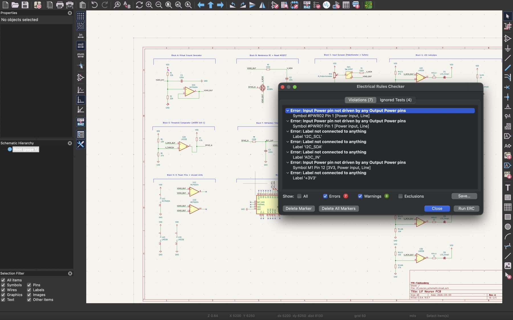
Some of the errors I had were unconnected labels and power pins not explicitly connected to output power pins. For the latter, I fixed it by adding a PWR_FLAG. In KiCad, a PWR_FLAG is a small symbol that explicitly tells the ERC "yes, this net is actually driven by a power source." Without it, KiCad sees a power net (like VDD or GND) with only passive components connected and raises an error because it can't verify anything is actually supplying that voltage. Placing a PWR_FLAG on the net resolves this.
After resolving all errors and warnings, the ERC passed clean.
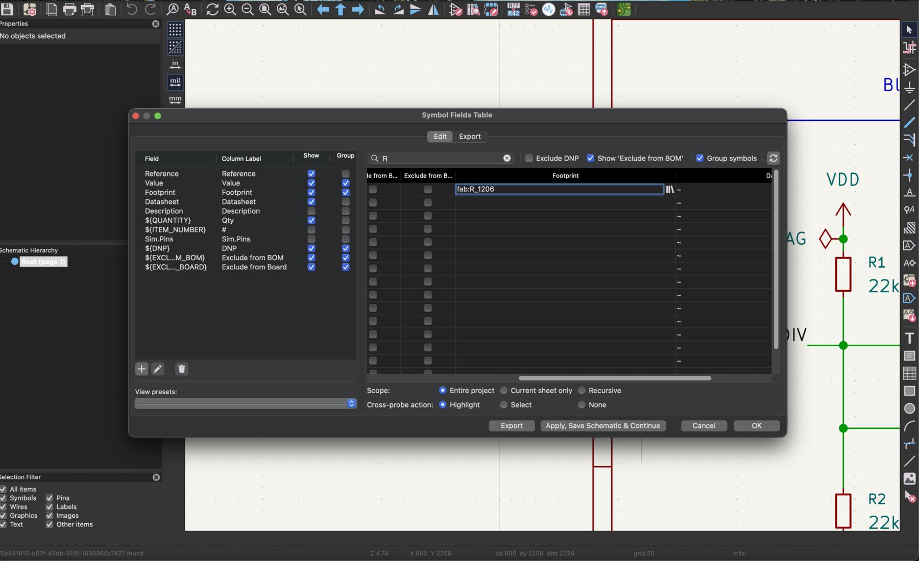
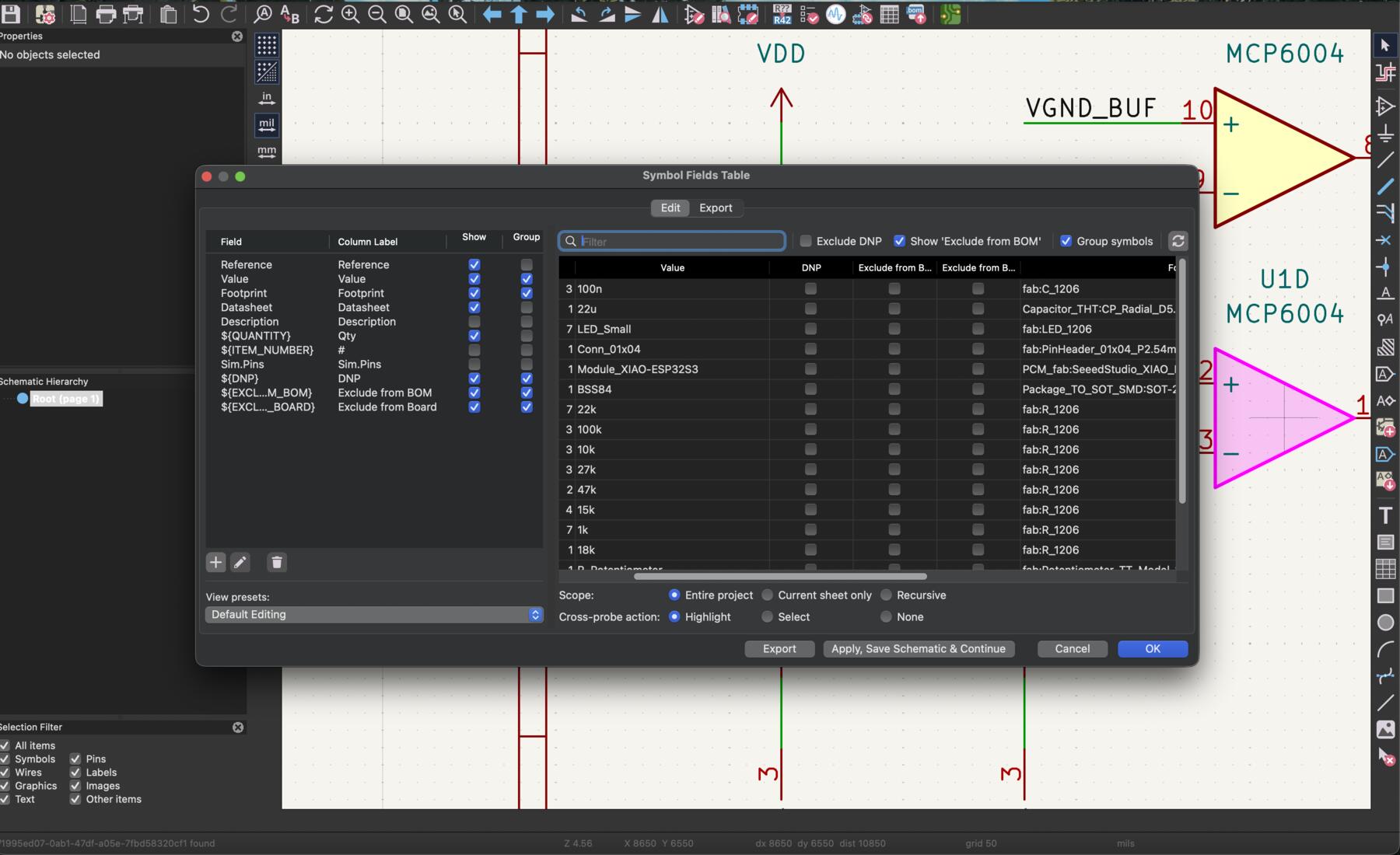
Additionally, I needed to map the symbols to footprints for the PCB design. Every schematic symbol needs a footprint assigned to it — the footprint tells KiCad the physical size and pad layout of the real component. To do this, I opened the Symbol Fields Table (Tools > Edit Symbol Fields), which shows all components in a spreadsheet view. For each component I selected the correct footprint from the Fab library based on the actual package I'd be using (e.g. a 0805 resistor gets the R_0805 footprint). Getting this right matters because mismatched footprints mean pads that don't line up with the physical part.
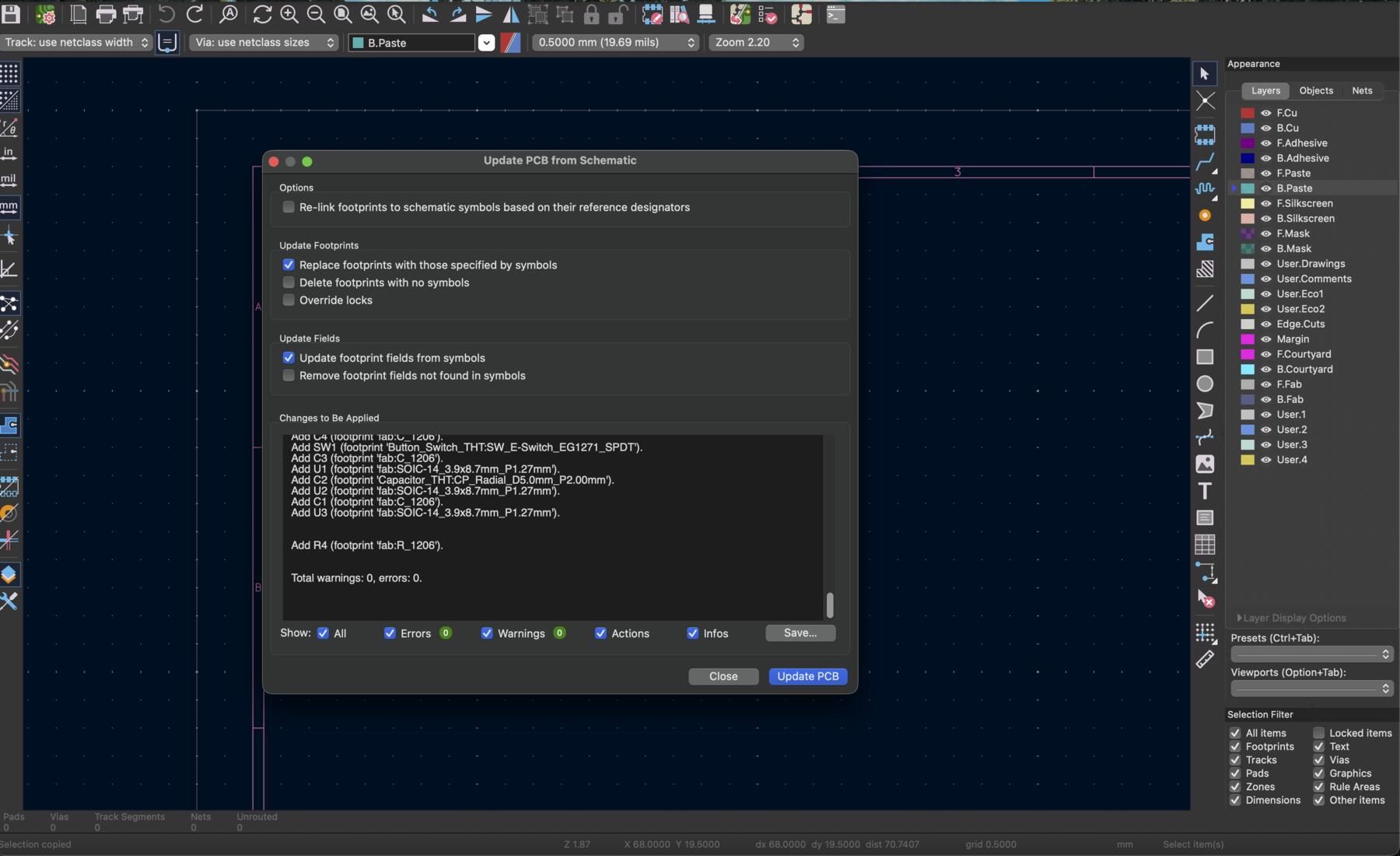
PCB Design
With the schematic complete and ERC passing, I moved to the PCB editor. In KiCad, you go to Tools and then Update PCB from Schematic, which imports all the component footprints and their connections (the "rats nest" of unrouted lines showing which pads need to be connected).
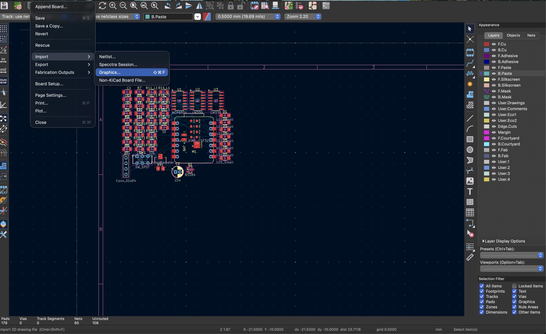
In KiCad's PCB editor, the Edge_Cuts layer defines the physical boundary of the board — it's the line the CNC mill follows when cutting the board out of the raw material. Any closed shape drawn on this layer becomes the board outline. I designed a custom neuron-shaped outline in Inkscape, exported it as an SVG, and imported it onto the Edge_Cuts layer — download board cutout SVG.
The first step was placing the components on the board. I grouped them by functional block, keeping the VGND generator components close together, the membrane RC section in the middle, the comparators near the LEDs they drive, and the input pot and switch near the board edge for easy access. Component placement is arguably the most important step in PCB layout because good placement makes routing much easier.
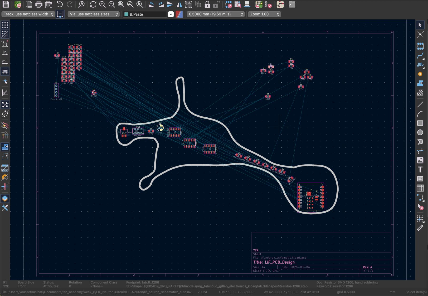
Then for routing, I needed to add certain constraints that would make it possible to fabricate this board with the equipment we have by setting the minimum clearance and track width to 0.2 mm.
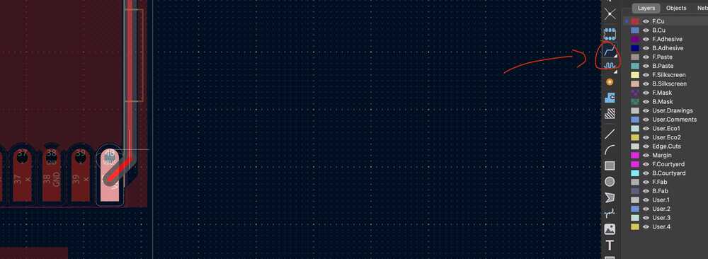
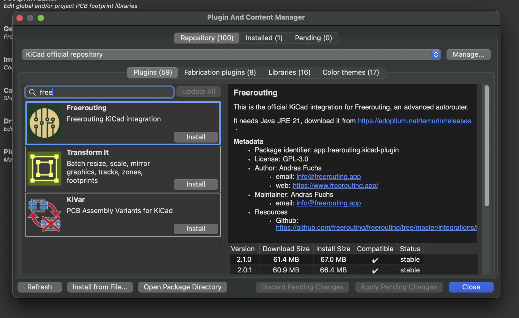
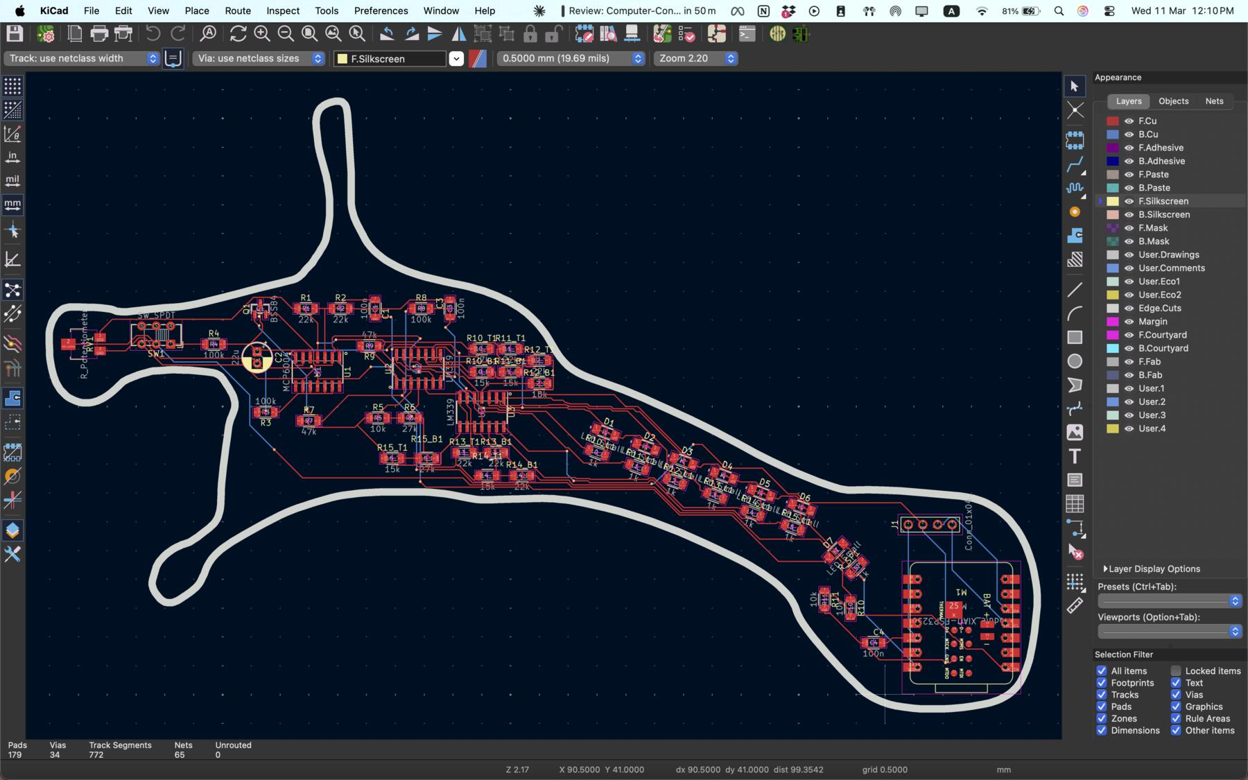
I started routing manually, but it was a bit exhausting due to the number of components and their placement (since some need to be place in specific places making the ratsnet even more essy). Thus, I utilized the Freerouting plugin to help me out.
The routing was completed and i was pretty content with the outcome even though it used the backside of the board too (highlighted in blue).
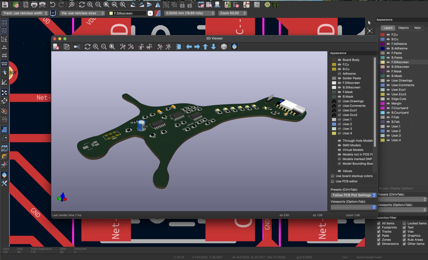
After routing, I used the 3D viewer in KiCad to check how the board would look physically. This is a useful sanity check to make sure components do not overlap and that the board makes sense mechanically.
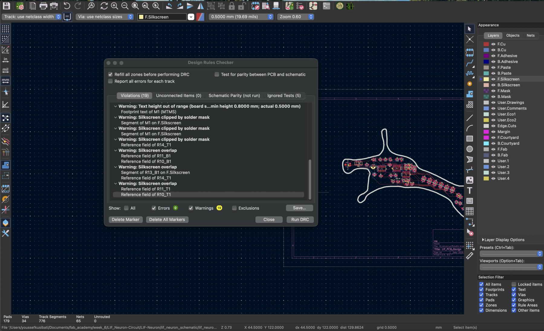
Design Rule Check
I ran the DRC (Design Rule Check) to verify that all traces meet the minimum width and clearance requirements for our fabrication process. The DRC checks for things like traces that are too close together, pads that are too small, unrouted connections, and violations of the design rules I specified. After fixing any violations that came up, the DRC passed clean.
The errors were for the text that I don't really need.
Manufacturing Check
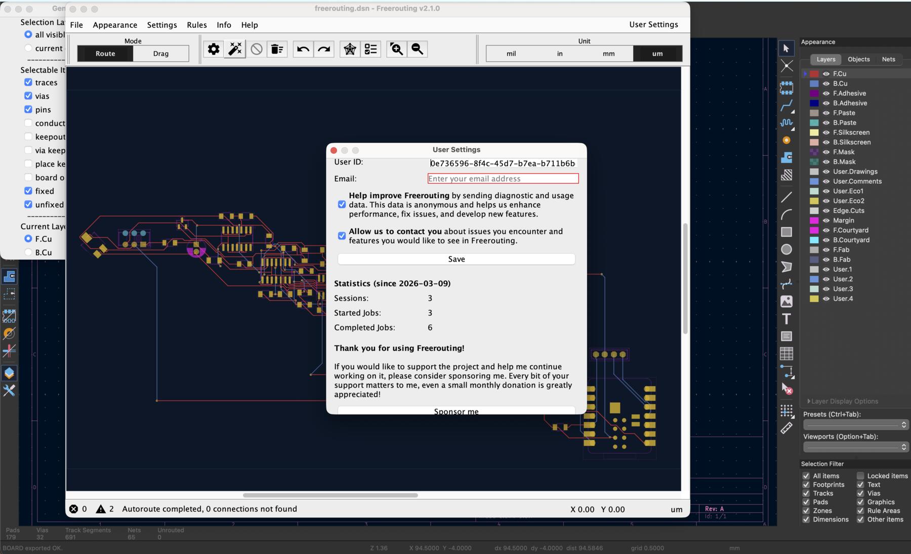
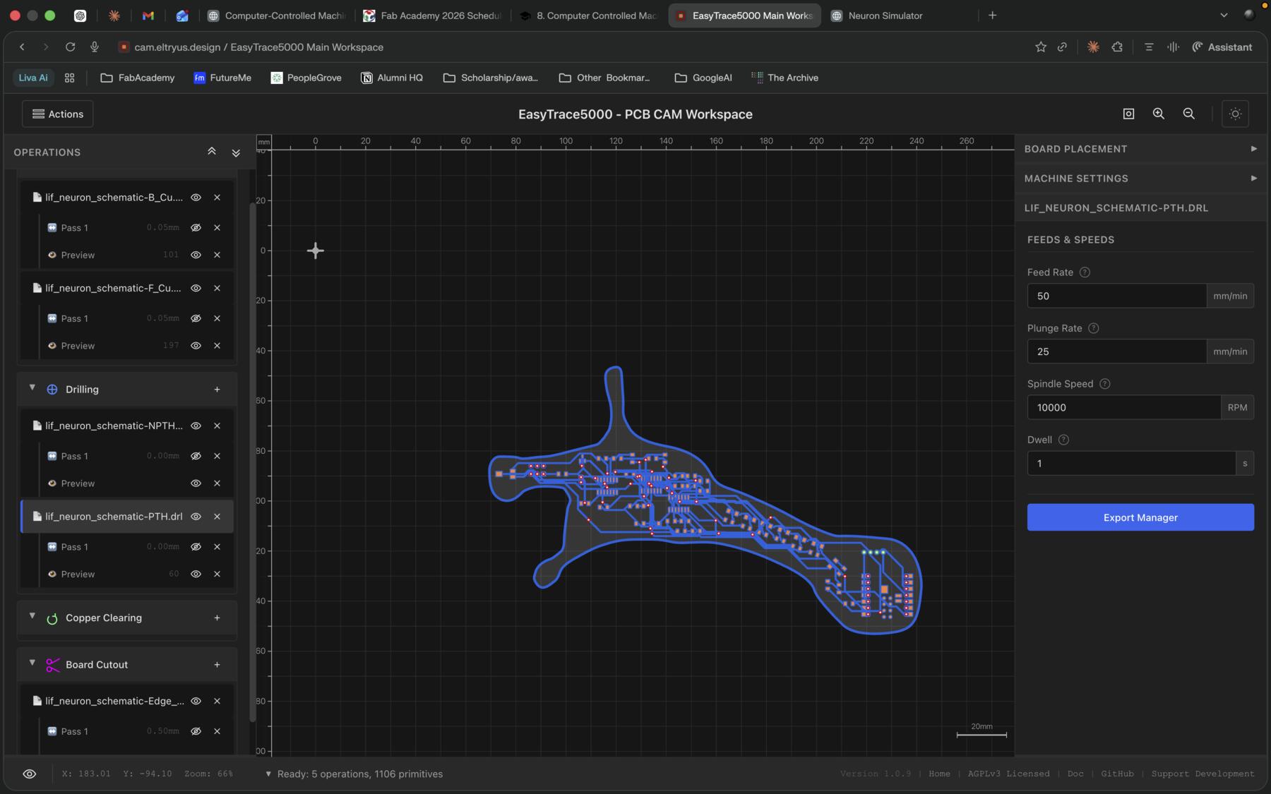
To verify that my PCB design could actually be fabricated, I used EasyTrace5000 to check the design against manufacturing constraints. Shoutout to my instructor Ricardo for developing this tool, which makes this process much easier than using MODs.
I started by exporting the Gerber files from KiCad.
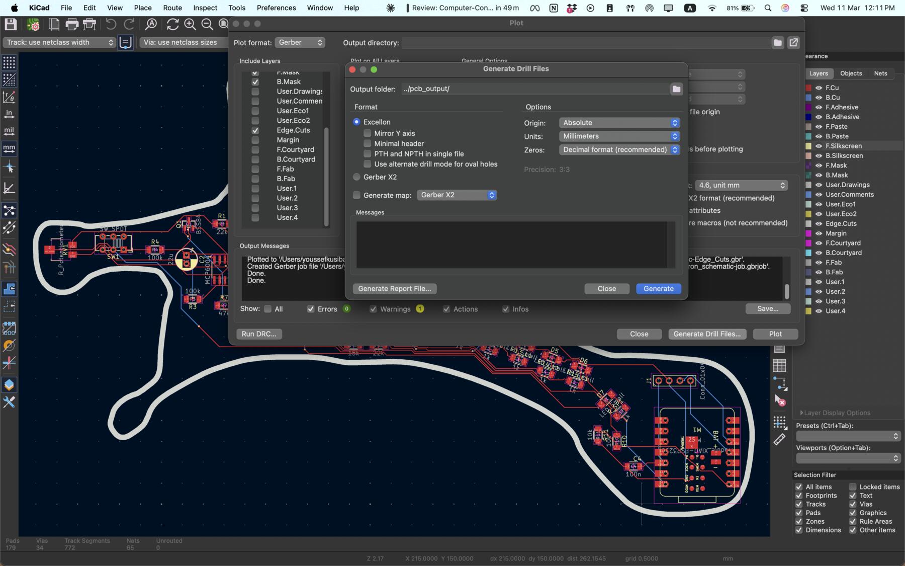
EasyTrace5000 analyzes the board layout and identifies any features that might cause problems during fabrication, such as traces that are too thin, clearances that are too tight, or drill holes that are too small for the available tooling. My design passed the manufacturing check, though my instructor noted that while the board could probably be made by a board house, the tiny vias the auto-router included would make it tricky to fabricate in a fablab setting.
Tutorials I Followed to Learn
Here is a list of some YouTube tutorials I checked out initially to learn how to design on KiCad, and of course, shoutout to my good friend Claude and Codex/ChatGPT for the explanations along the way.
https://youtu.be/Q-yT332uCWY?si=HLQENXo80psA3QAt
https://www.youtube.com/watch?v=O-zNn5k5Bn4
https://www.youtube.com/watch?v=igQWdVGZGpI
https://www.youtube.com/watch?v=L6YZDuvRC90
https://www.youtube.com/watch?v=jiJGbWOSdMo
https://www.youtube.com/watch?v=LO9AO0XTX3M
https://www.youtube.com/watch?v=b-7bMl6fJio
Original Design Files
This Week's Checklist
- Linked to the group assignment page
- Documented what you have learned in electronics design
- Checked your board can be fabricated
- Explained problems and how you fixed them
- Included original design files (Eagle, KiCad, etc.)
- Included a 'hero shot'