Fab Academy Logo
EN | PT
EN | PT

Week 6: Testing and Observing the Operation of a Microcontroller Circuit Board

Group Assignment

Testing a Microcontroller Circuit Board

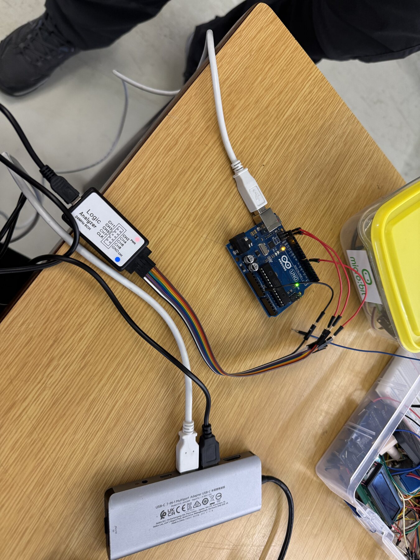
This group assignment was about understanding how a microcontroller board behaves electrically, not only that the code "runs." At the most basic level, a microcontroller communicates with the outside world by changing voltage over time. If we can observe those voltage changes, we can verify timing, protocol behavior, and signal quality.

  • Logic analyzer test to decode digital communication (I2C)
  • Oscilloscope test to observe waveform behavior (PWM)

Testing the Logic Analyzer

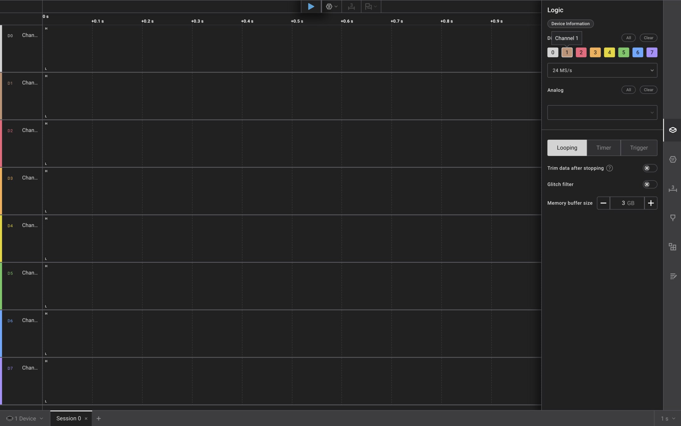
A logic analyzer is best when the signal is digital and protocol-based. It samples high/low states and lets us decode communication buses such as I2C.

  • SCL is the clock line (defines when bits are sampled)
  • SDA is the data line (carries address/data/ACK bits)
  • A transfer starts with a START condition and ends with a STOP condition
  • Each byte is followed by an ACK/NACK bit

So this test answers: is the microcontroller generating valid I2C traffic with consistent timing?

Test Setup

  • Board: Arduino Uno
  • Logic analyzer + Logic 2 software
  • Sketch: Uno as I2C master, transmit every 500 ms to address 0x3C
  • Marker pin D7 toggled each transmission for timing correlation
Logic Analyzer Setup

Wiring

  • Uno A4 (SDA) → Analyzer D0
  • Uno A5 (SCL) → Analyzer D1
  • Uno D7 → Analyzer D2 (timing marker)
  • Uno GND → Analyzer GND
Logic Analyzer Wiring

Logic 2 Configuration

  • Sample rate: 2 MS/s
  • I2C analyzer added with: SDA = D0, SCL = D1, 7-bit addressing
Logic 2 Screenshot

What We Observed

  • Repeating activity every ~500 ms
  • Marker pin D7 toggled at the same cadence
  • I2C decoder showed: Setup Write to [0x3C] + NAK
  • Bus clock around 100 kHz
Logic 2 Screenshot 2

Interpreting the Result

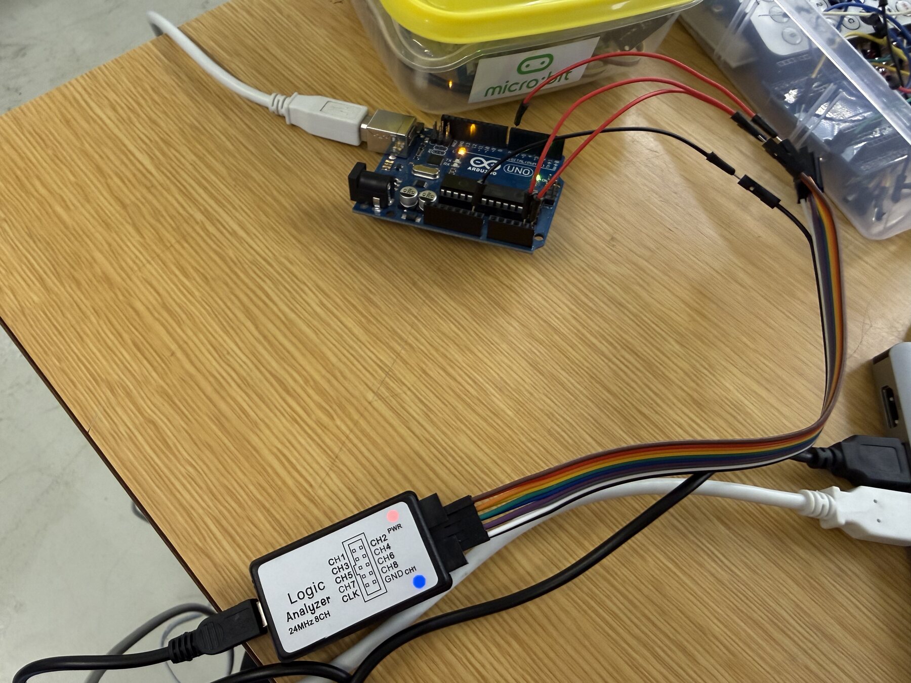
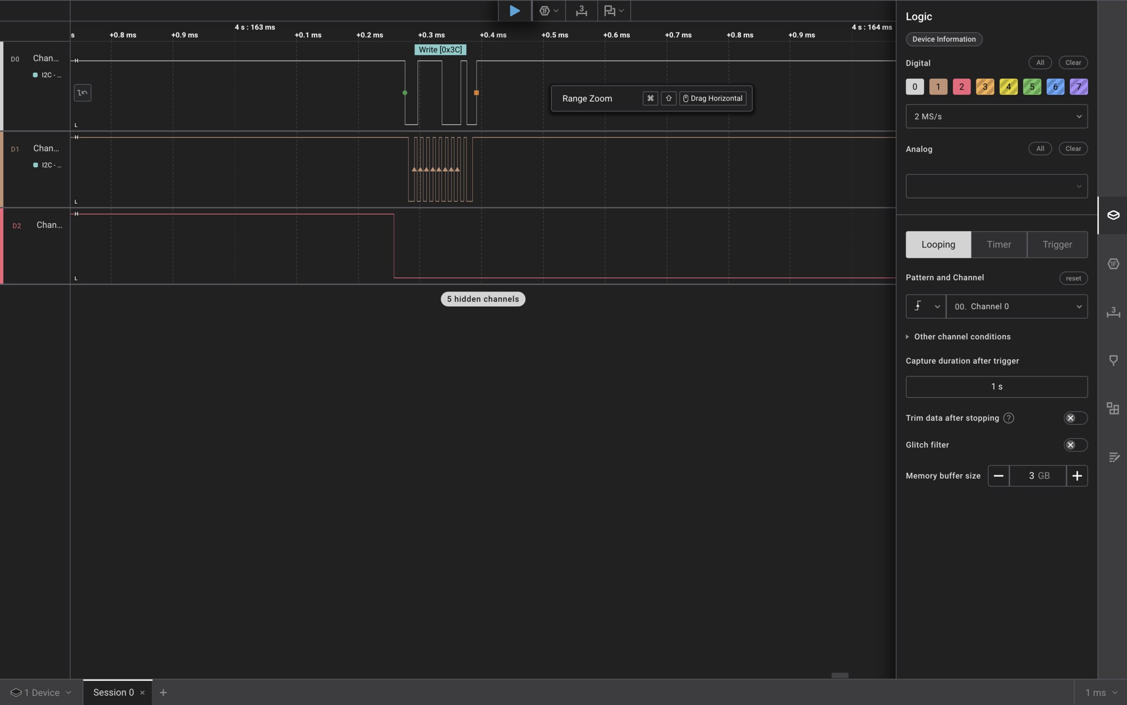
This NAK is expected in our setup because we intentionally tested on an empty bus (no slave connected). The microcontroller still generated valid I2C timing and addressing, which is exactly what we wanted to verify at this stage.

  • Correct I2C signal generation
  • Correct timing periodicity
  • Correct protocol decoding in Logic 2

Testing the Oscilloscope

An oscilloscope lets us inspect the analog shape of voltage vs time. For PWM, that is important because PWM is fundamentally a time-domain signal:

  • Frequency stays mostly constant
  • Duty cycle changes the average delivered power

So this test answers: is the board producing a stable PWM waveform, and does the duty-cycle change behave as expected?

Test Sketch and Behavior

We used a simple PWM ramp on Uno pin D9:

analogWrite(9, x)
x increments every 250 ms
resets after 255

This creates a duty-cycle sweep from ~0% to ~100%, repeating continuously.

Wiring

  • Oscilloscope probe tip → Uno D9
  • Oscilloscope ground clip → Uno GND
Oscilloscope Wiring

What We Observed

  • Stable PWM waveform at around Uno default PWM frequency (~490 Hz)
  • Pulse width gradually increased every 250 ms
  • After reaching near full duty, it reset and repeated
  • Full duty ramp period was about 256 × 250 ms ≈ 64 s
Oscilloscope Screenshot

Interpreting the Result

  • Timer-driven PWM frequency remained stable
  • Duty changed predictably with the incrementing x

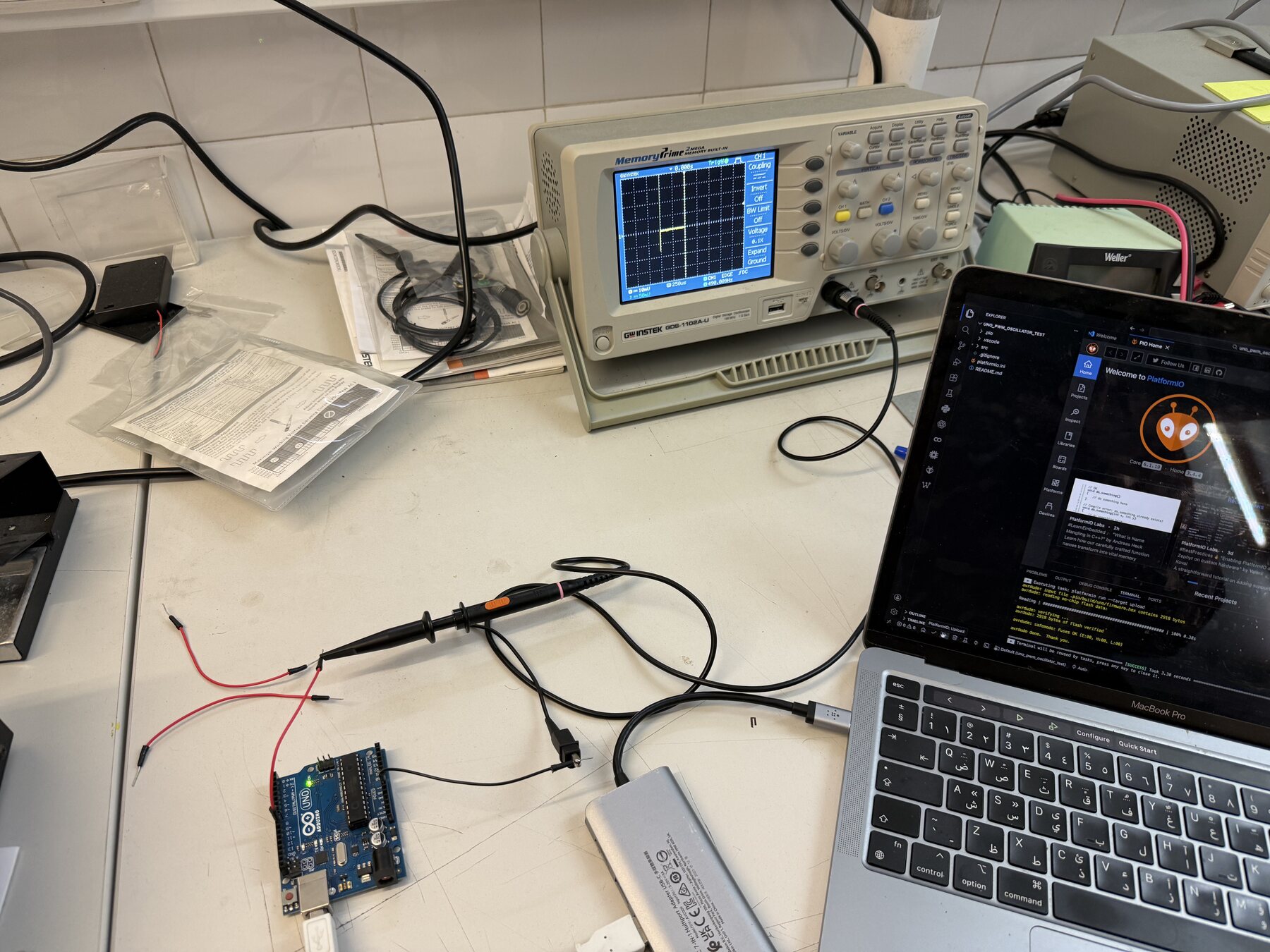
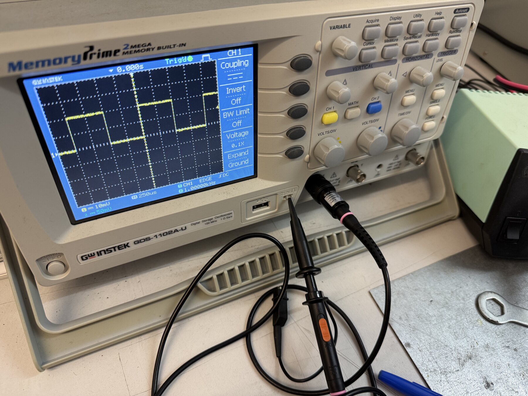
The oscilloscope test confirmed that the microcontroller output timing is stable and that PWM control is behaving correctly.