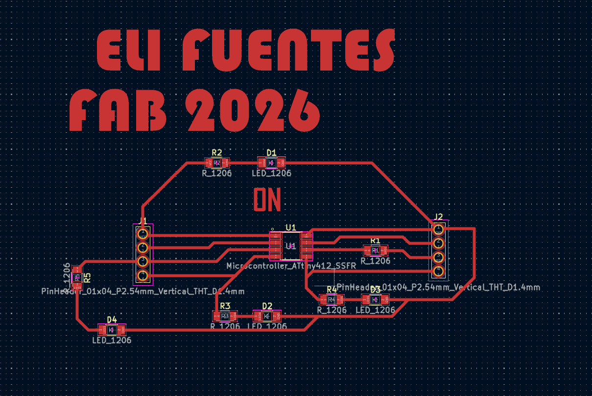
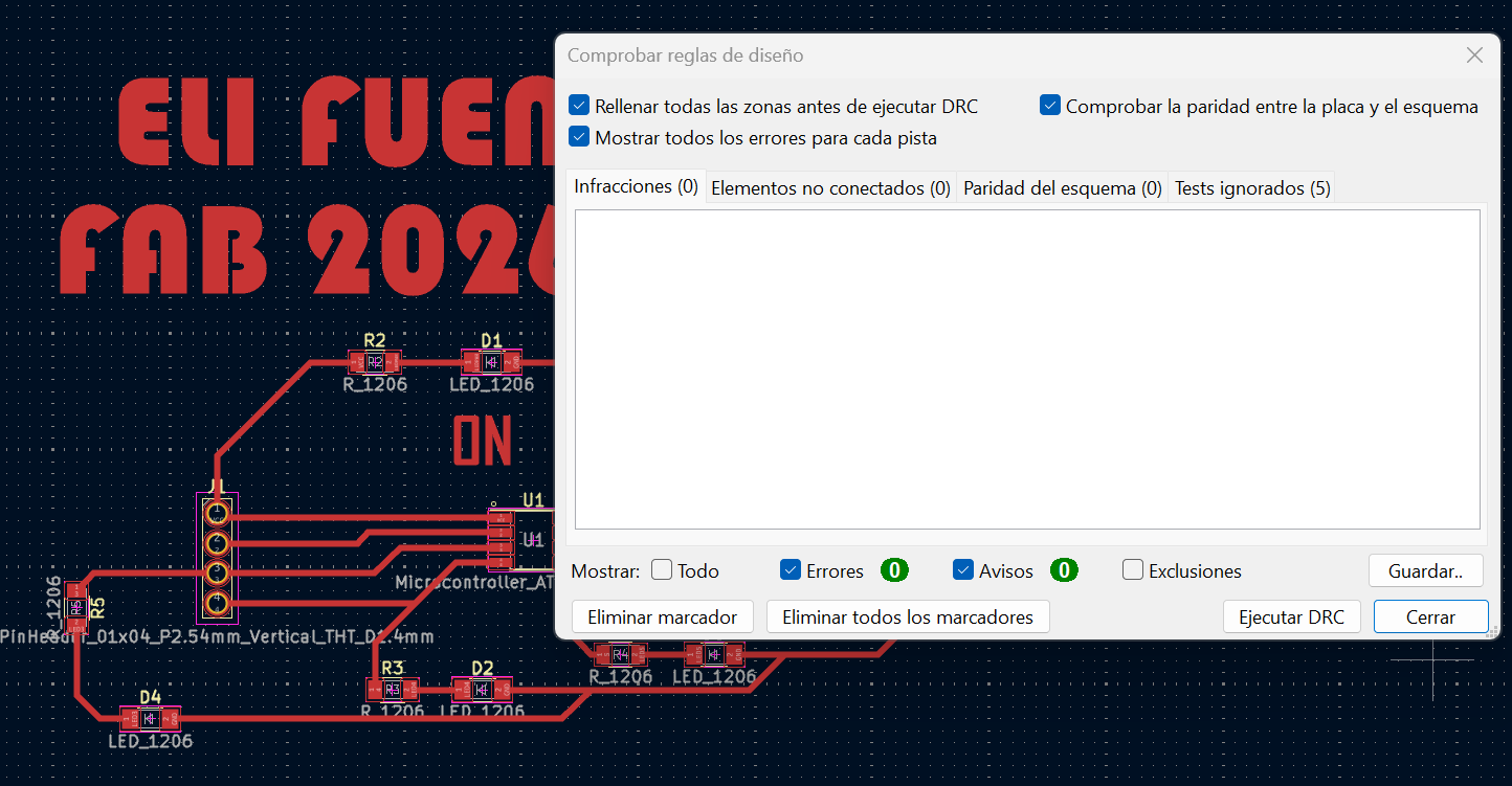
For this assignment, we designed a custom development board
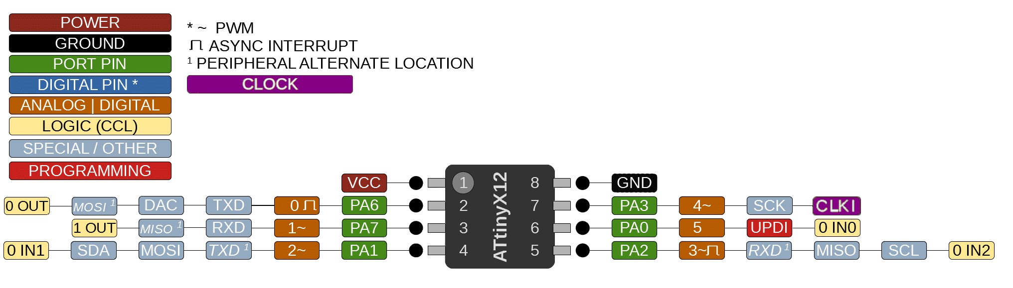
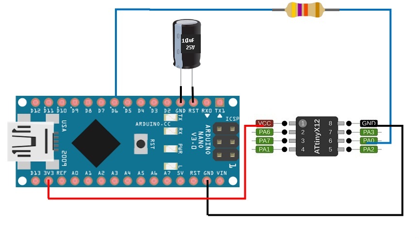
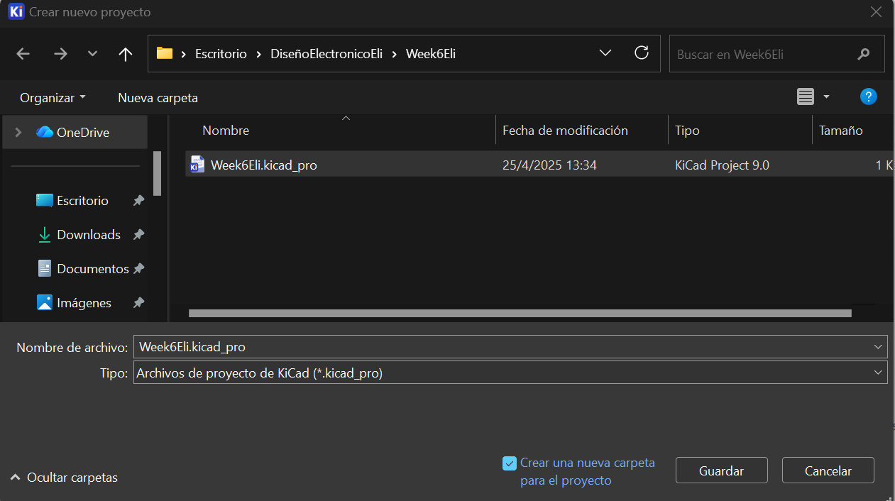
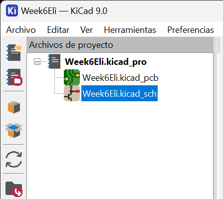
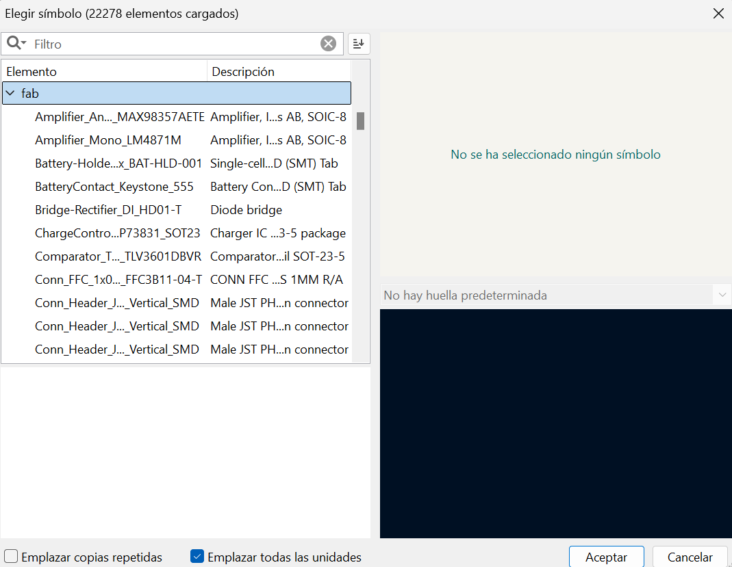
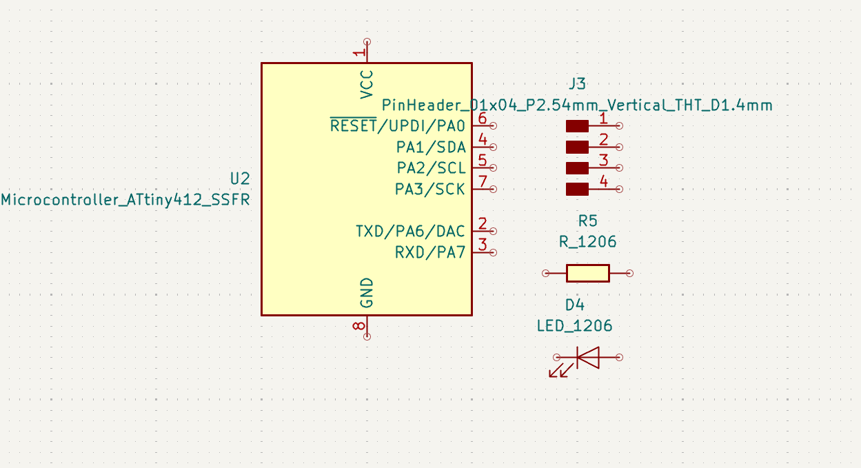
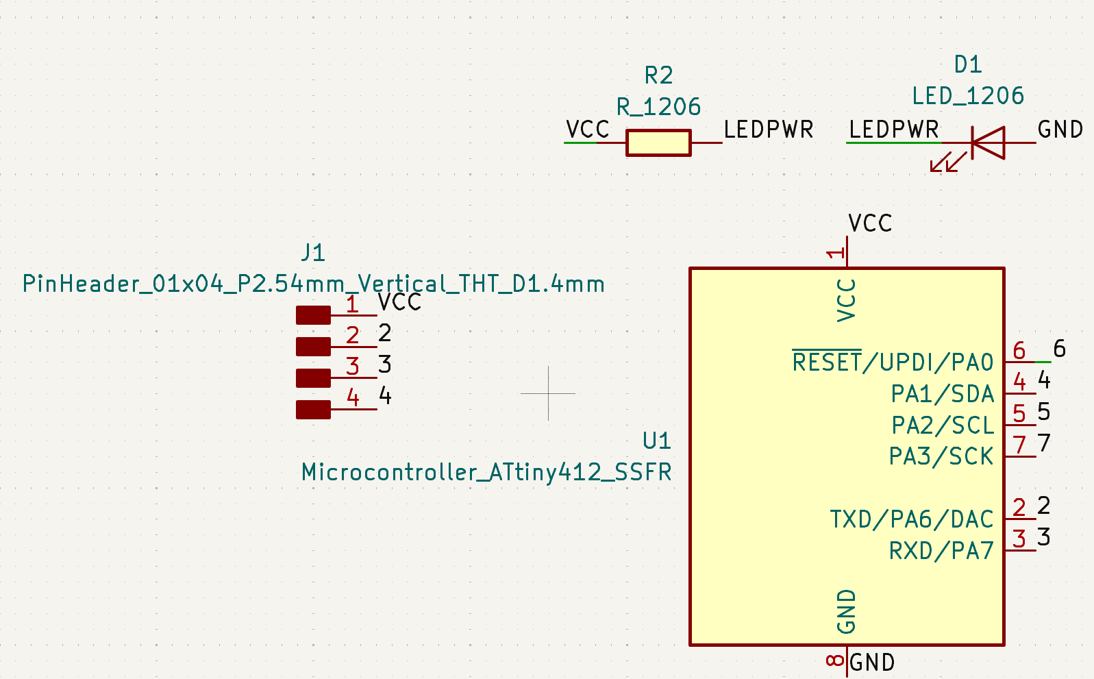
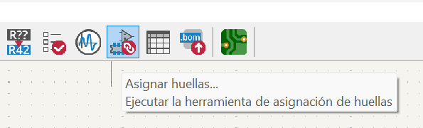
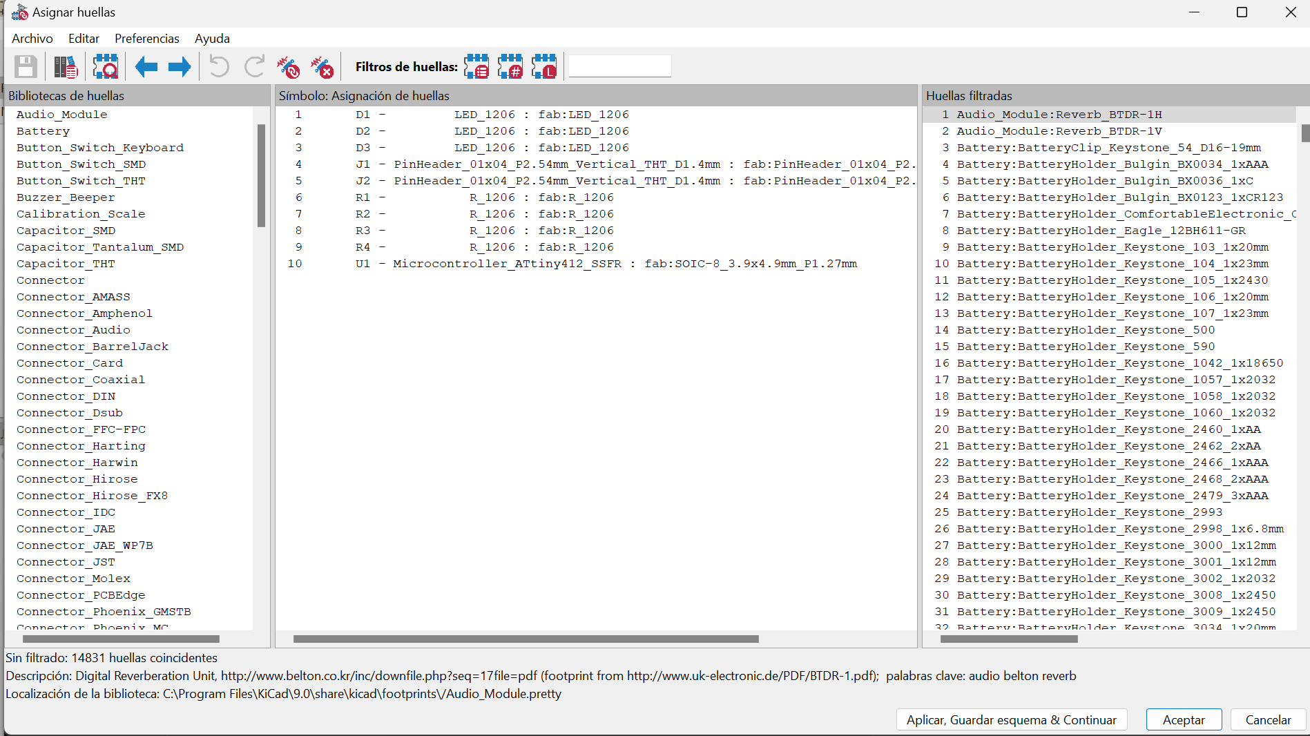
 based on the ATtiny412 microcontroller. This board integrates several electronic components that allow multiple functionalities. The entire process was carried out using KiCad, an EDA software that enables schematic design and PCB layout generation.

Image 02

The ATtiny412 is an 8-bit microcontroller based on the AVR architecture. It is designed for low-power and compact applications. It features 8 pins, 4 KB of Flash memory, 256 bytes of SRAM, and uses a UPDI interface for programming and debugging through a single pin.

Image 20

To upload the program, we use the UPDI interface (pin 6) together with an Arduino Nano, as shown in the schematic.

Image 21
Image 03

1. Installation

We installed KiCad, an open-source EDA software with a simple installation process.

Image 1

2. Library Download

We downloaded the Fab Academy component library from the official repository and extracted it into a specific folder.

Image 2

3. Adding Symbol Libraries

We added the symbol libraries through Preferences → Manage Symbol Libraries, linking the fab.kicad_sym file.

Image 3

4. Adding Footprint Libraries

Similarly, we added footprint libraries through Preferences → Manage Footprint Libraries.

Image 4

5. Project Creation

We created a new project and saved it in a designated folder.

Image 5

6. Schematic Design

We opened the schematic file (.sch) to begin the circuit design.

Image 6

7. Component Placement

Using the “Place Symbols” tool, we accessed and selected components from the libraries.

Image 7

8. Component Selection

We added all required components into the workspace.

Image 8

9. Component Overview

All components used were from the Fab library.

Image 9

10. Net Labeling

We assigned labels to define connections between components.

Image 10

11. Footprint Check

We verified that each component had an assigned footprint.

Image 11

12. Footprint Verification

Missing footprints were assigned manually from the library.

Image 12

13. PCB Update

We updated the PCB layout to display components and connections.

Image 13

14. Routing

We routed all connections following proper track widths and electronic design rules. The circuit includes LEDs on pins 4 and 5 to visualize outputs, a resistor on pin 6 for UPDI programming, and a power indicator LED.

Image 14

15. Design Rule Check

We performed a DRC (Design Rule Check) to ensure the board has no errors and is ready for fabrication.

Image 15

Results

As a result, we successfully designed a functional PCB based on the ATtiny412 microcontroller. The circuit integrates output LEDs, a programming interface via UPDI, and a power indicator. The design passed all DRC validations, confirming that it is ready for manufacturing.

Conclusion

This assignment allowed us to develop a deeper understanding of electronic design workflows, from schematic creation to PCB layout. We reinforced our knowledge of components, libraries, and design rules, while gaining practical experience using KiCad. The process highlighted the importance of precision and verification in ensuring a functional and manufacturable electronic design.