Electronics Production

This week focuses on PCB fabrication — milling circuit boards in-house, characterizing the production process, and making and testing a microcontroller development board.

Assignment Requirements

Group Assignment:

Individual Assignment:

Project Documentation

For the individual assignment, I produced a microcontroller development board based on the XIAO ESP32-C6. I took the provided Gerber files, generated the G-code using the Carvera software, milled the board on our Carvera desktop CNC mill, soldered the components, and tested it.

Design to G-Code Workflow

The workflow for producing this board:

  1. Started with the provided Gerber files (F.Cu for copper traces, Edge_Cuts for the board outline)
  2. Imported the Gerber files into the Carvera desktop software (MakerCAM)
  3. Converted the Gerber files to G-code toolpaths for trace isolation and board outline
  4. Exported the final .nc G-code file and sent it to the Carvera for milling

Milling the Board

I milled the board on our Carvera desktop CNC mill by Makera. It's a compact 3-axis CNC designed for PCB milling, wood, and soft metals.

Carvera Specs
  • Work area: 200 × 150 × 60 mm
  • Spindle speed: 1,000–12,000 RPM
  • Positioning accuracy: ±0.01 mm
  • Tool changer: Automatic 4-tool carousel
  • Probing: Automatic Z-probe for PCB leveling
  • Software: MakerCAM (built-in CAM for Gerber → G-code)
  • Vendor: Makera — Carvera Desktop CNC

The Carvera software (MakerCAM) handled the conversion from Gerber to G-code, generating the toolpaths for trace isolation and the board outline cut.

Milling the XIAO ESP32-C6 board on the Carvera
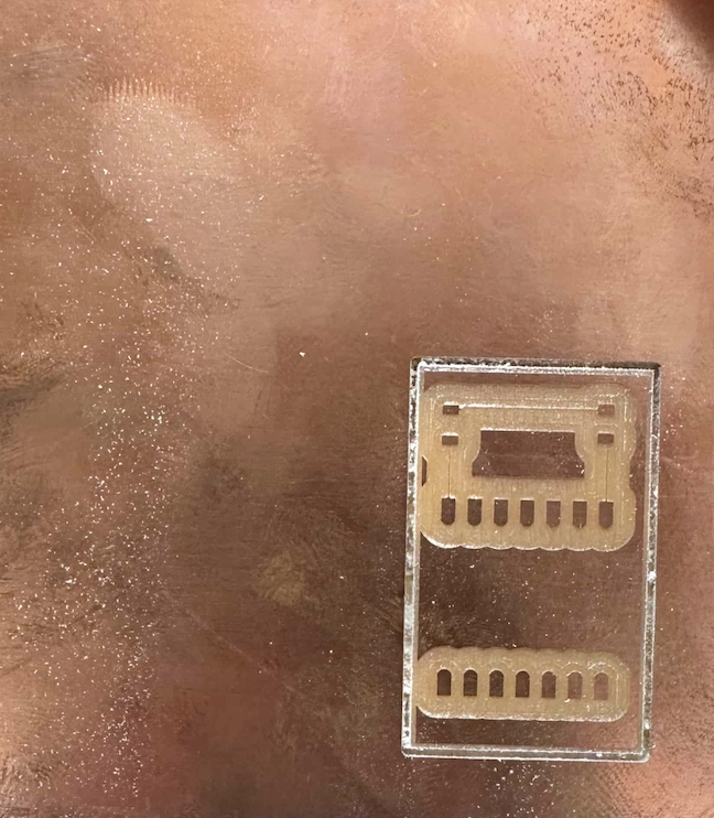
CNC milled XIAO ESP32-C6 development board

CNC milled XIAO ESP32-C6 development board on the Carvera

Design Files

📦 F.Cu Gerber (Traces) 📦 Edge Cuts Gerber (Outline) 📦 G-Code (.nc)

Soldering

After milling, I hand-soldered the pin headers and components onto the board. I don't have video of this process since it's nearly impossible to hold a camera steady while soldering — you need both hands for the iron and the solder.

My soldering technique for these CNC-milled copper boards:

  • Solder paste first: I apply a fair amount of solder paste to the pads before placing components, especially on milled copper boards. The copper traces on a milled PCB don't have the plated-through holes or solder mask that commercial boards have, so the paste helps the solder flow and bond properly to the raw copper surface.
  • Fine wire solder: I use very thin gauge solder wire for the actual joints. Thin wire gives much better control over how much solder you're applying — on small pads and tight traces, too much solder can easily bridge between adjacent traces and create shorts. With fine wire, you can feed just a tiny amount at a time.
  • Clean tip: Keeping the soldering iron tip clean and tinned is critical on milled boards. A dirty tip doesn't transfer heat efficiently, which means you end up holding the iron on the pad longer, risking damage to the copper trace (which can delaminate from the FR4 substrate if overheated).
  • Flux: The solder paste contains flux, which cleans the copper surface and helps the solder wet properly. On milled boards, the copper oxidizes quickly after cutting, so flux is essential for getting good joints.

Testing — LED Blink

After soldering the components onto the milled board, I wrote a simple blink program to verify that the board was working correctly. The code toggles an LED connected to GPIO17 (pin D7) on and off every 500ms. I uploaded the code to the XIAO ESP32-C6 using the Arduino IDE — for details on how to set up the Arduino IDE for the ESP32-C6 and upload code, see Week 4 — Embedded Programming.

// LED Blink Test — XIAO ESP32-C6 Custom PCB
// Toggles LED on GPIO17 (D7) every 500ms to verify board functionality

#define LED_PIN 17   // D7 = GPIO17

void setup() {
  pinMode(LED_PIN, OUTPUT);
}

void loop() {
  digitalWrite(LED_PIN, HIGH); // LED ON
  delay(500);
  digitalWrite(LED_PIN, LOW);  // LED OFF
  delay(500);
}

How the Code Works

  • GPIO17 (D7): This is the pin connected to the LED on the custom PCB. The #define maps it to a readable name.
  • setup(): Configures GPIO17 as an output pin so it can drive the LED.
  • loop(): Continuously toggles the pin HIGH (3.3V, LED on) and LOW (0V, LED off) with a 500ms delay between each state — creating a 1Hz blink pattern.

Board Test — LED Blinking

LED blinking on the custom milled PCB — board test successful
Our lab uses a Carvera desktop CNC mill for in-house PCB production. The workflow for going from KiCad design files to a milled board uses MakerCAM to generate the toolpaths. The process involves three separate toolpaths: one for the copper traces, one for drilling component holes, and one for cutting the board outline.

Phase 1: Project & Stock Setup

  1. Open MakerCAM and select New Project.
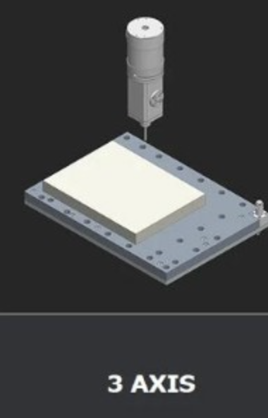
  2. On the welcome screen, choose a 3-axis project.
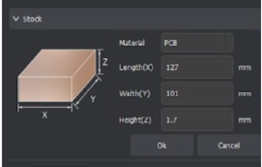
  3. In the Stock Setup panel, click "Edit" and enter the PCB stock dimensions:
    • Material: PCB
    • Length (X): 127 mm
    • Width (Y): 101 mm
    • Height (Z): 1.7 mm
MakerCAM project setup — 3-axis selection

MakerCAM — 3-axis project setup

MakerCAM stock material setup for PCB

MakerCAM — stock material dimensions for the PCB

Phase 2: Import Your Design

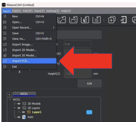
  1. Go to File → Import → Import PCB (KiCad Gerber & Drill).
  2. Import your three files one by one:
    • Edge_Cuts file (board outline)
    • F.Cu file (copper traces)
    • PTH.drl file (drill holes)
MakerCAM importing Gerber files

MakerCAM — importing Gerber and drill files

Phase 3: Position & Create Trace Toolpath

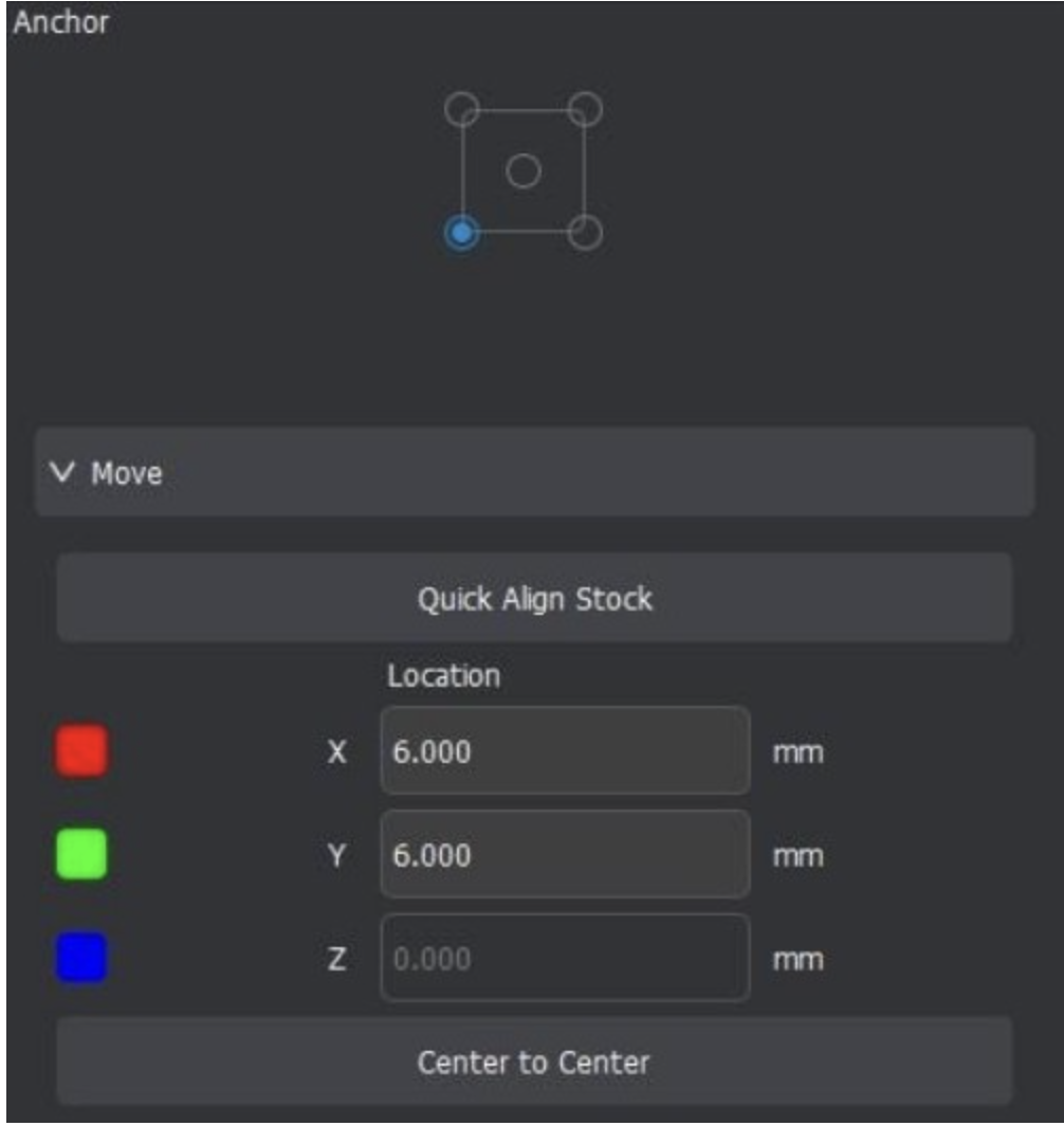
Your design may appear off-screen after import — zoom out to find it. Select the entire design (it will become dotted), press M to move, set the anchor to the lower-left corner, and position it at X: 6.000, Y: 6.000 to give clearance from the stock edges.

Important tip: A trace is selected when you see a dotted line. If the line is solid, it is not selected.

MakerCAM positioning the PCB design on the stock

MakerCAM — positioning the board on the stock

For the trace toolpath:

  1. Make only the F.Cu and Edge_Cuts layers visible.
  2. Hold Shift and click both layers to select them.
  3. Hold Shift and click the outermost outline to deselect it (it turns solid) — only the traces and inner outline should remain selected (dotted).
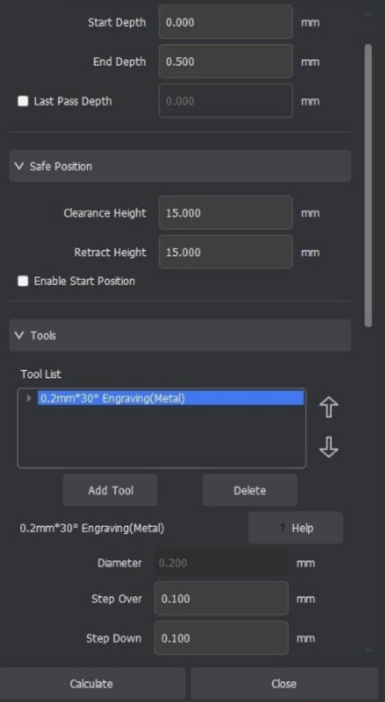
  4. Select the 2D Pocket tool from the toolbar.
  5. Set cutting depth: Start 0.000 mm, End 0.05 mm.
  6. Add tools:
    • Tool 1: 0.8mm corn end mill
    • Tool 2: 0.2mm 30-degree engraving bit (metal)
    Make sure the 0.8mm bit is listed first.
  7. Set path strategy to Parallel.
  8. Click Calculate.
MakerCAM trace isolation toolpath setup

MakerCAM — trace isolation toolpath calculated

Phase 4: Drill Holes Toolpath

  1. Hide everything except the PTH.drl (drill) layers.
  2. Select the 2D Drilling tool from the toolbar.
  3. Select all visible drill holes.
  4. Set cutting depth: Start 0.000 mm, End 1.7 mm (full board thickness).
  5. Choose the 0.8mm corn bit.
  6. Click Calculate.

Phase 5: Board Outline Toolpath

  1. Hide everything except the Edge_Cuts layer.
  2. Select the 2D Contour tool from the toolbar.
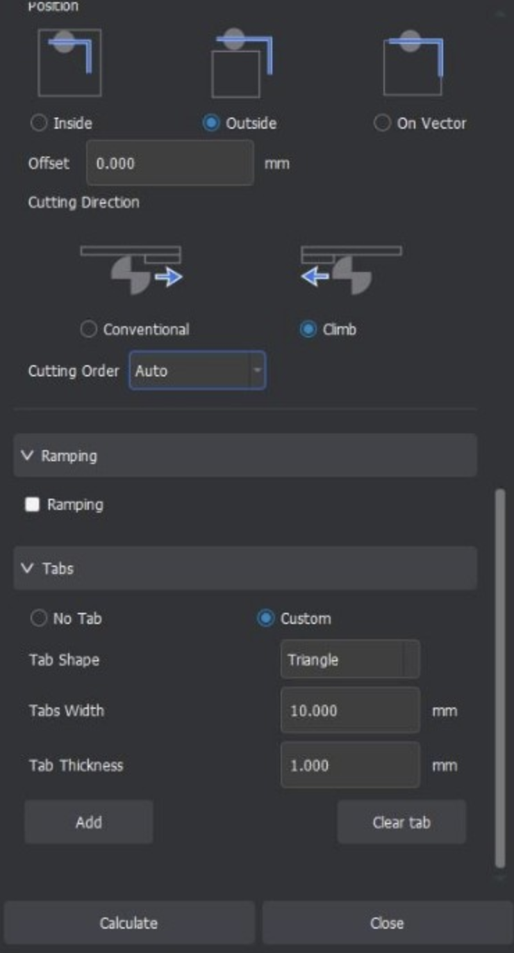
  3. Click the outside line to deselect it — the inside line must remain dotted.
  4. Set cutting depth: Start 0.000 mm, End 1.7 mm.
  5. Choose the 0.8mm corn bit.
  6. Set strategy to Outside.
  7. Scroll to Tabs, select Custom, and click Add — place 3–4 tabs on the board edges to hold it in place during the final cut.
  8. Click Calculate.

Phase 6: Simulate & Export

  1. Click the Preview Toolpaths icon.
  2. Check all three toolpaths (Pocket, Drilling, Contour) and click Preview to watch the simulation.
  3. Close the preview and click the Export icon.
  4. Select all three toolpaths and export as a .nc g-code file.
MakerCAM toolpath generation

MakerCAM — generating toolpaths for all operations

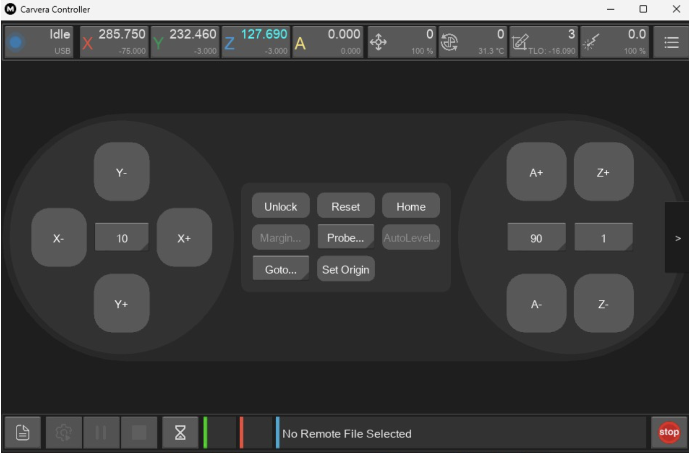
Makera Carvera controller interface

Makera Carvera controller — sending the job to the machine

Reference

📄 MakerCAM Workflow Guide (PDF)

For the week 8 group assignment, our team characterized the design rules for our in-house PCB production process and documented the workflow for sending a PCB to a board house. You can view the full group page here: Week 8 Group Assignment.

My Contributions

My contribution to the group assignment was documenting the MakerCAM workflow for our Carvera desktop CNC mill. I walked through the full process from importing KiCad Gerber and drill files into MakerCAM, setting up stock dimensions, positioning the design, and creating the three toolpaths needed to produce a board: trace isolation, drilling, and board outline. I documented each phase with the specific settings and tool selections so other students in the lab can follow the same workflow.

Useful Links