For the individual assignment I used KiCad 9.0 as my EDA tool to design a custom 8x8 LED matrix board. The matrix uses surface mount LEDs and is designed to interact and communicate with an Arduino Uno.
Why an LED Matrix?
An LED matrix is a good project for learning EDA because it involves repetitive but precise component placement, multi-layer routing, and direct microcontroller interfacing. The 8x8 grid gives you 64 individually addressable LEDs using only 16 I/O pins through multiplexing — each LED sits at the intersection of a row and column, and you light it by driving the correct row HIGH and column LOW.
Design Decisions
I decided to go with an 8x8 matrix — 64 LEDs total — which is a straightforward multiplexed design. The circuit itself is fairly simple: 8 rows and 8 columns, with each LED addressed by activating the correct row and column combination. The board interacts and communicates with an Arduino Uno (ATmega328P microcontroller), which drives the matrix using 16 of its I/O pins — digital pins D2 through D13 for 12 of the lines, plus analog pins A0 through A3 (used as digital outputs) for the remaining 4.
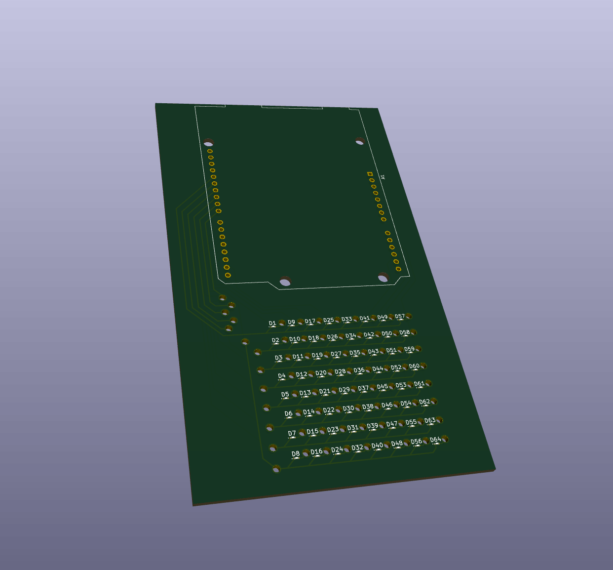
The board is a two-sided PCB, which was necessary to route all the traces without running into each other. Row traces run on the front copper layer (F.Cu) and column traces on the back copper layer (B.Cu), with 77 vias connecting signals between the two sides where needed.
Design Journey — Intermediate Steps
The final board didn't come together in one shot. Here's the progression of decisions and iterations I went through:
Phase 1 — Research and Planning
- Started by researching multiplexing techniques — read about Charlieplexing vs traditional row-column scanning and decided traditional was better for this project (simpler wiring, higher brightness, easier to solder)
- Calculated pin requirements: 8 rows + 8 columns = 16 pins. Arduino Uno has exactly enough (D2-D13 + A0-A3)
- Decided on 0603 SMD LEDs for compact layout — initially considered 0402 but rejected it as too small for hand soldering 64 units
- Chose two-layer PCB early on because routing 8 rows and 8 columns on a single layer would create impossible crossings
Phase 2 — Schematic Iteration
- First attempt at the schematic was messy — 64 LEDs with direct wires everywhere made it unreadable
- Switched to net labels (ROW1-8, COL1-8) which cleaned up the schematic dramatically
- Used copy-paste for LED placement (Ctrl+C, Ctrl+V) — KiCad auto-increments reference designators which saved significant time
- Ran ERC multiple times during schematic development to catch wiring errors early
Phase 3 — PCB Layout Challenges
- First PCB attempt: placed LEDs roughly by hand, tried auto-router — result was a mess of tangled traces with DRC violations everywhere
- Second attempt: calculated exact grid coordinates (3mm spacing) and manually positioned all 64 LEDs using the properties dialog. Tedious but produced a perfect grid
- Routing strategy evolved: started trying to route everything on one layer, quickly realized it was impossible. Adopted the "rows on front, columns on back" strategy which made routing straightforward
- Via placement was iterative — started with too many vias, then optimized by rethinking trace paths to reduce layer changes
- Ran DRC after every major routing session. Initial runs showed 12+ clearance violations; fixed by adjusting trace positions and via locations until DRC passed clean
Phase 4 — Verification and Refinement
- Used KiCad's 3D viewer extensively to check component placement and verify nothing was overlapping
- Verified manufacturability through MODS — confirmed all traces and clearances are within CNC milling capabilities
- Final DRC: 0 errors, 0 warnings. Final ERC: 0 errors (warnings about undriven power pins are expected for Arduino module)
Note: I completed this project earlier in the semester and don't have screenshots of every intermediate state. The documentation above describes the actual progression of decisions and iterations I went through. The final schematic, PCB layout, and 3D model shown below represent the end result of this iterative process.
Schematic Design Workflow
I started in KiCad's schematic editor (Eeschema) by placing the Arduino Uno R3 module symbol and all 64 LED symbols. Each row of 8 LEDs shares a common anode connection, and each column shares a common cathode. The schematic is straightforward but large — wiring 64 LEDs with proper net labels for all 8 rows and 8 columns took careful organization to keep it readable.
Adding Symbols to the Schematic
To add a symbol in KiCad's schematic editor:
- Press 'A' key or click "Add Symbol" button — this opens the symbol chooser dialog
- Search for the component — I typed "LED" to find the LED symbol, and "Arduino_UNO_R3" for the Arduino module
- Select and place — Click the symbol you want, then click on the schematic canvas to place it
- Repeat for all components — I placed 64 LED symbols (8 rows × 8 columns) and 1 Arduino Uno R3 module
For repetitive components like the 64 LEDs, I used copy and paste (Ctrl+C, Ctrl+V) to speed up placement. KiCad automatically increments reference designators (LED1, LED2, LED3...) which saved a lot of time.
Wiring and Net Labels
After placing all symbols, I wired them together:
- Press 'W' key to start drawing a wire
- Click to place wire segments connecting component pins
- Add net labels (Press 'L') to name connections — I used labels like "ROW1", "ROW2"... "ROW8" for the 8 row lines and "COL1", "COL2"... "COL8" for the 8 column lines
- Connect to Arduino pins — Wired ROW1-8 to Arduino pins D2-D9, and COL1-8 to pins D10-D13 and A0-A3
Net labels are crucial for complex schematics — instead of drawing wires across the entire page, you label both ends of a connection with the same name and KiCad knows they're electrically connected.
Assigning Footprints
After completing the schematic, I assigned physical footprints to each symbol:
- Open "Assign Footprints" tool (Tools → Assign Footprints, or click the footprint icon)
- For each LED: Selected
LED_SMD:LED_0603_1608Metric_Pad0.64x0.40mm_HandSolder- 0603 size (1.6mm × 0.8mm) — small enough for compact layout, large enough to hand solder
- "HandSolder" variant has extended pads (0.64mm × 0.40mm) making manual soldering easier
- For Arduino: Selected
Module:Arduino_UNO_R3— includes mounting holes and proper pin spacing - Save and update PCB — Click "Apply, Save Schematic & Continue" to push footprints to the PCB editor
Changing Footprints
If you need to change a footprint after assignment:
- In schematic editor: Double-click the symbol → "Footprint" field → Click browse button → Select new footprint
- Or use Assign Footprints tool: Select component in left pane → Choose new footprint in right pane → Apply
- Update PCB: Tools → Update PCB from Schematic (F8) — this pushes the footprint change to the board layout
I initially tried a smaller 0402 footprint but switched to 0603 after realizing hand soldering 64 tiny 0402 LEDs would be extremely difficult.
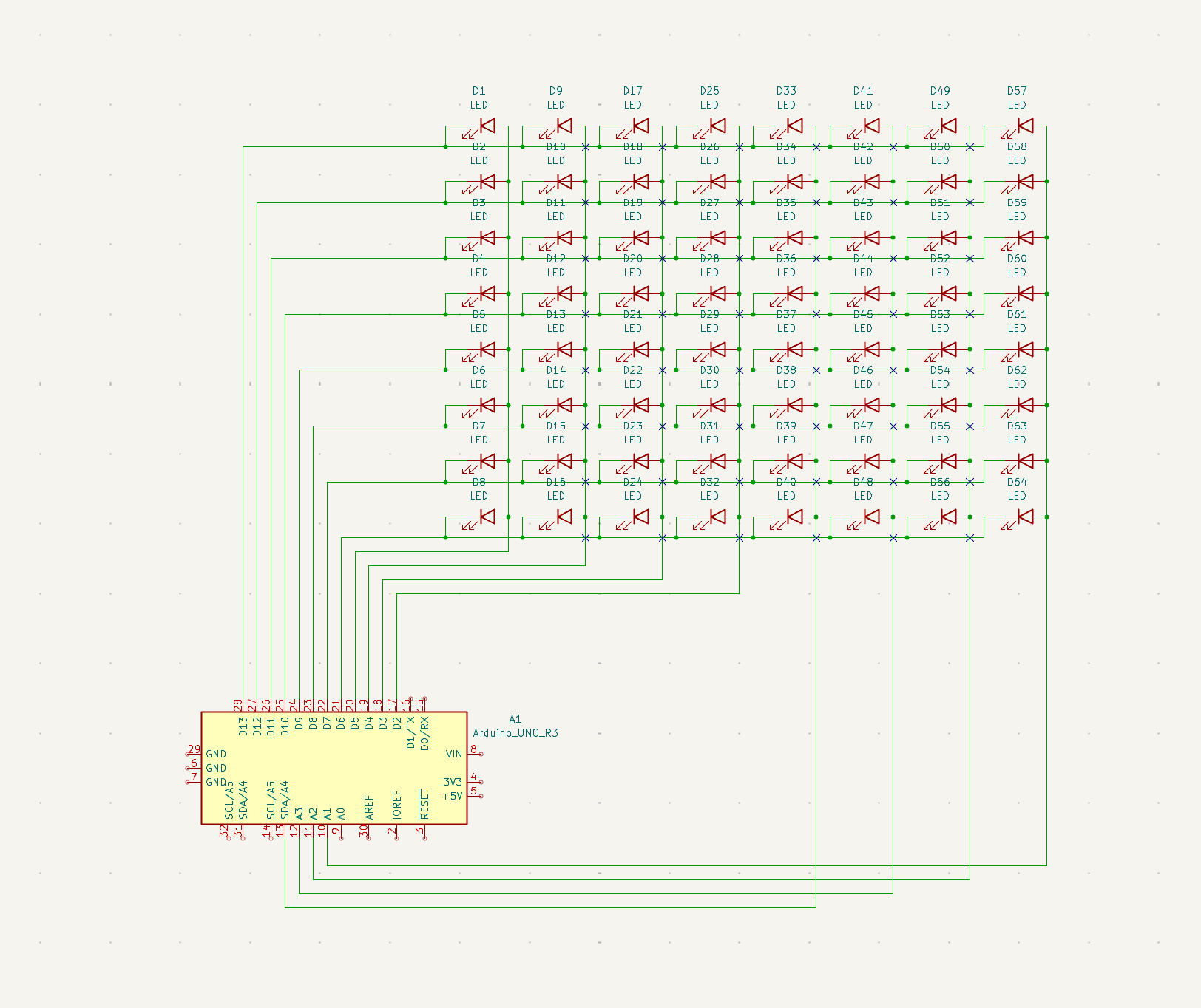
KiCad schematic — 8x8 LED matrix controlled by Arduino Uno with net labels for rows and columns
PCB Layout — LED Arrangement Process
The most time-consuming part was the PCB editor. After assigning footprints and updating the PCB from the schematic (Tools → Update PCB from Schematic, or press F8), all 64 LED footprints and the Arduino module appeared on the board canvas in a jumbled pile.
Arranging the 8x8 LED Grid
Getting 64 surface mount LEDs into a perfect 8x8 grid was the biggest challenge of this project. Here's how I did it:
- Calculate grid spacing:
- LED footprint size: 1.6mm × 0.8mm (0603 package)
- Decided on 3mm center-to-center spacing for both X and Y axes
- This gives 1.4mm clearance between LEDs — enough for traces and vias
- Set grid origin: Chose starting point at X=20mm, Y=20mm (top-left corner of matrix)
- Calculate all 64 positions:
- Row 1: Y = 20mm, X = 20, 23, 26, 29, 32, 35, 38, 41mm
- Row 2: Y = 23mm, X = 20, 23, 26, 29, 32, 35, 38, 41mm
- ...and so on for all 8 rows
- Position each LED manually:
- Select LED footprint → Press 'E' to edit properties
- Enter exact X and Y coordinates in the Position fields
- Repeat for all 64 LEDs — tedious but necessary for perfect alignment
Why manual positioning? KiCad doesn't have a built-in "arrange in grid" tool for footprints. There's no way to select 64 components and automatically snap them into an 8×8 layout with even spacing. I tried using the grid snap feature, but it doesn't work well for precise matrix layouts — any small offset compounds across the grid. Manual coordinate entry was the only way to guarantee perfect alignment.
Routing Traces
After positioning all LEDs, I routed the copper traces connecting them:
- Press 'X' key to start routing a trace
- Click on a pad to start the trace, then click to place route segments
- Switch layers: Press 'V' key while routing to place a via and switch to the opposite copper layer
- Complete the route: Click on the destination pad to finish
Layer strategy:
- Front copper (F.Cu): All row connections — horizontal traces connecting LED anodes in each row
- Back copper (B.Cu): All column connections — vertical traces connecting LED cathodes in each column
- Vias: 77 vias total to connect traces between layers where needed
I routed manually instead of using the auto-router because the auto-router struggled with the dense grid and created messy, inefficient paths. Manual routing gave me full control over trace aesthetics and ensured clean, professional-looking copper layers.
Trace Width Setup
Setting appropriate trace widths is critical for manufacturability and electrical performance:
- Open Board Setup: File → Board Setup → Design Rules → Net Classes
- Default net class settings:
- Trace width: 0.25mm (10 mils) — standard for signal traces on PCBs
- Clearance: 0.2mm (8 mils) — minimum spacing between copper features
- Via size: 0.8mm diameter, 0.4mm drill — standard plated through-hole via
- Why these values?
- 0.25mm traces are wide enough to carry LED current (~20mA per LED) without overheating
- 0.2mm clearance prevents shorts during milling and ensures reliable manufacturing
- Most PCB manufacturers can handle these dimensions easily
For power traces (if I had added power distribution), I would use wider traces (0.5mm or more) to handle higher current, but for this LED matrix all traces are signal-level and 0.25mm is appropriate.
Design Rule Check (DRC) and Electrical Rule Check (ERC)
Before finalizing the board, I ran KiCad's built-in checks to verify the design meets manufacturing and electrical requirements:
Electrical Rule Check (ERC) — Schematic
In the schematic editor:
- Click "Perform Electrical Rules Check" icon (or Inspect → Electrical Rules Checker)
- Click "Run ERC" button
- Review results:
- Checks for unconnected pins, conflicting pin types, missing power connections
- My design showed 0 errors — all LEDs properly connected to rows/columns, Arduino pins correctly wired
- Had a few warnings about "power pins not driven" which I ignored since the Arduino provides power externally
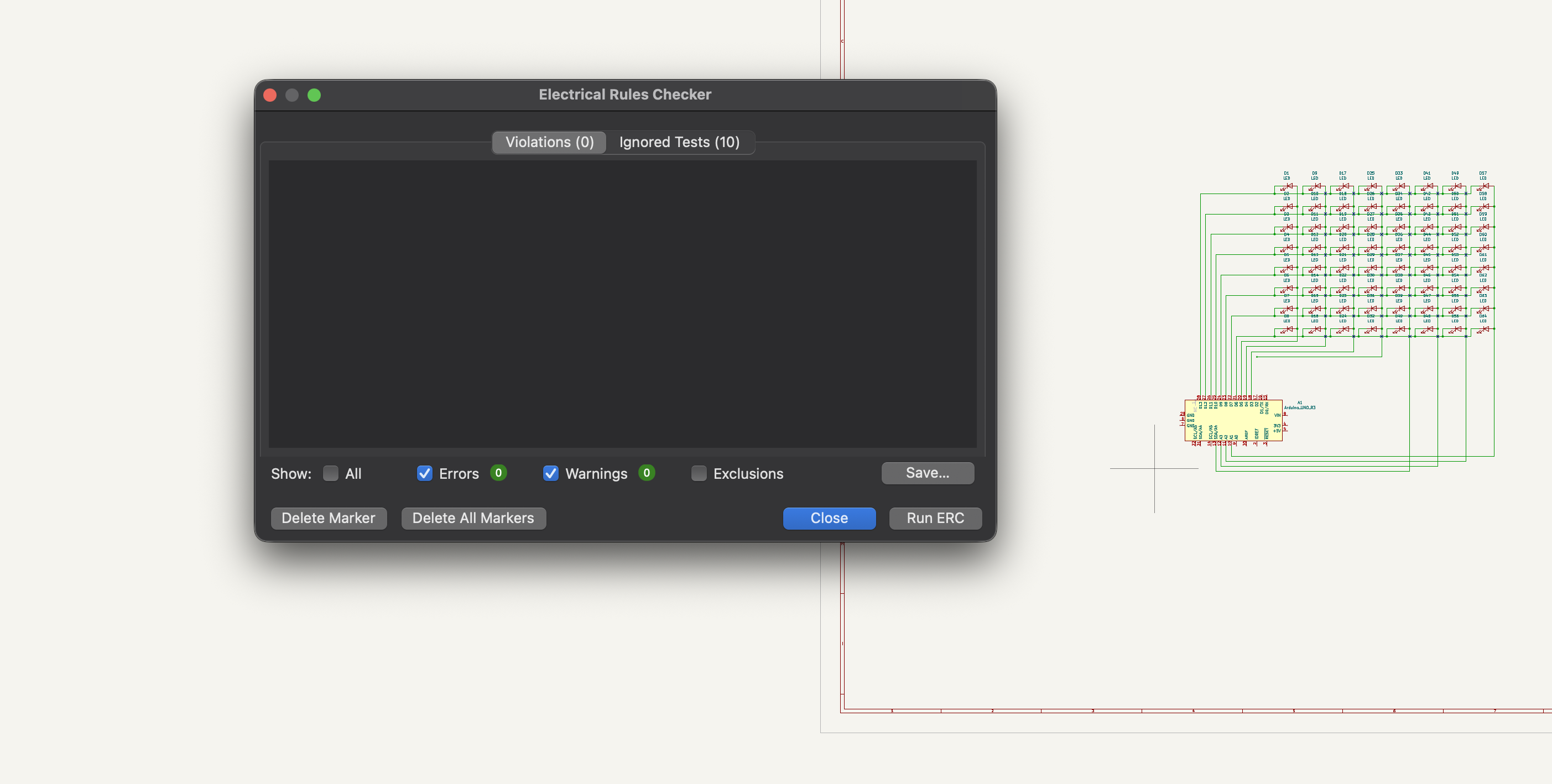
KiCad Electrical Rule Check — verifying the schematic has no wiring errors
Design Rule Check (DRC) — PCB Layout
In the PCB editor:
- Click "Perform Design Rules Check" icon (or Inspect → Design Rules Checker)
- Click "Run DRC" button
- Review violations:
- Checks for trace clearance violations, drill size errors, copper-to-edge clearance
- Initial run showed 12 clearance violations where traces were too close
- Fixed by rerouting problem traces and adjusting via positions
- Final DRC: 0 errors, 0 warnings — board is manufacturable
Why DRC/ERC matter: These checks catch mistakes before you send the board to manufacturing. A clearance violation could cause a short circuit. An unconnected pin means the circuit won't work. Running these checks is essential for any professional PCB design.
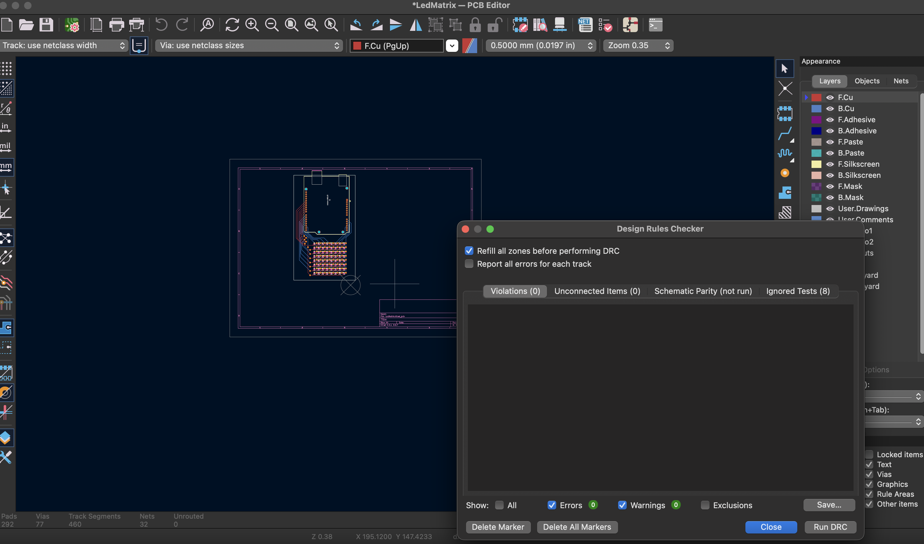
KiCad Design Rule Check — verifying trace clearances and manufacturing constraints
Creating the Board Outline
The board outline defines the physical edge of the PCB:
- Switch to Edge.Cuts layer: Select "Edge.Cuts" from the layer dropdown (or press Page Down to cycle layers)
- Draw the outline:
- Used the "Draw Rectangle" tool (right toolbar) to create a rectangular board
- Sized to 70mm × 70mm — large enough for the 8×8 LED grid plus Arduino mounting area
- Positioned to leave 5mm margin around components
- Alternative methods:
- Can use "Draw Line" tool for custom shapes
- Can use "Draw Arc" for rounded corners
- Edge.Cuts layer is special — anything drawn here defines where the board will be cut
The board outline must be a closed shape with no gaps. KiCad's DRC will flag any discontinuities in the Edge.Cuts layer.
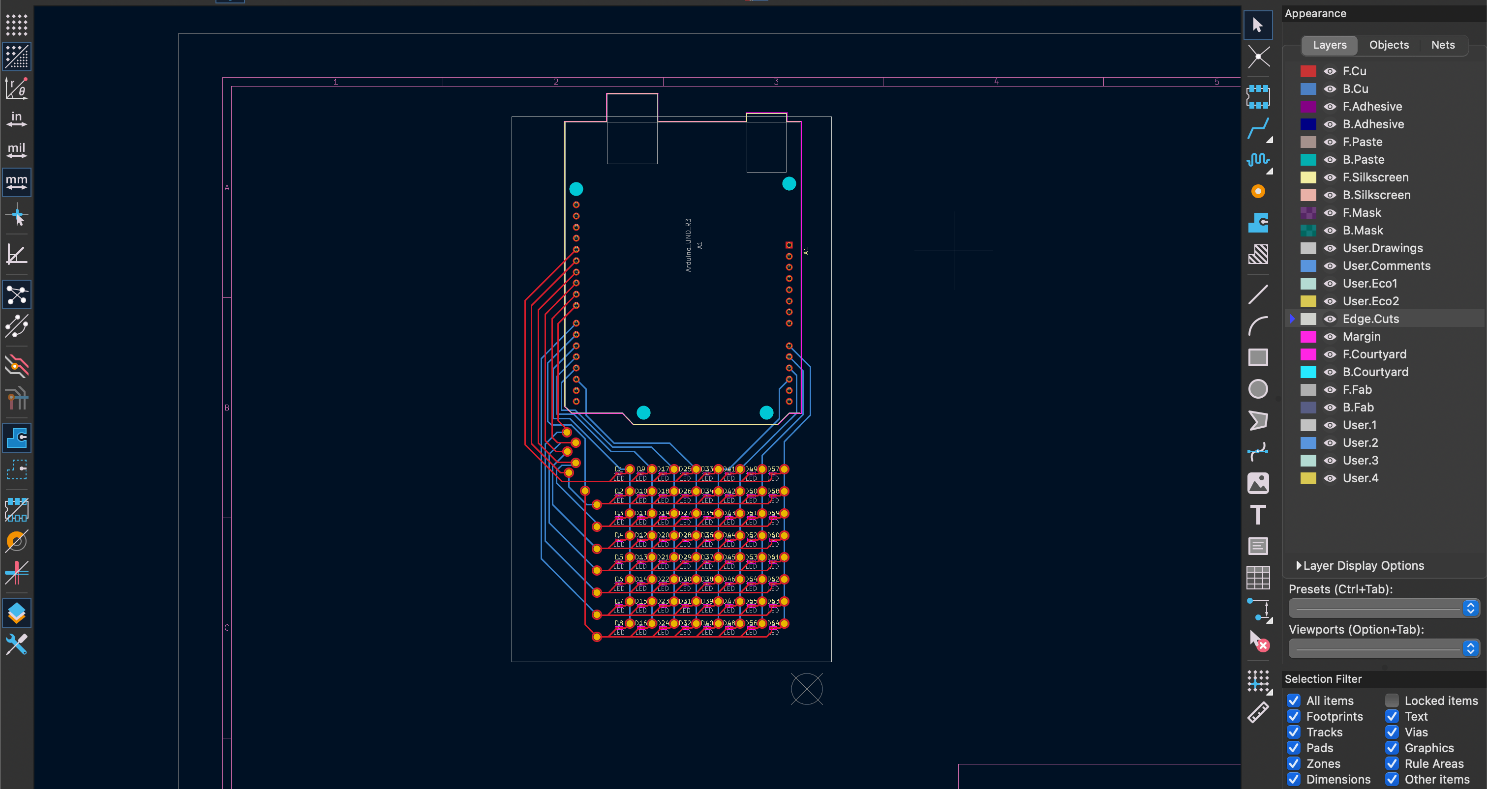
KiCad PCB editor — two-sided board layout with 64 LEDs and 77 vias
3D Board Preview
KiCad 3D viewer — the finished two-sided LED matrix board
-F_Cu.svg)
-B_Cu.svg)
-Edge_Cuts.svg)