Overview
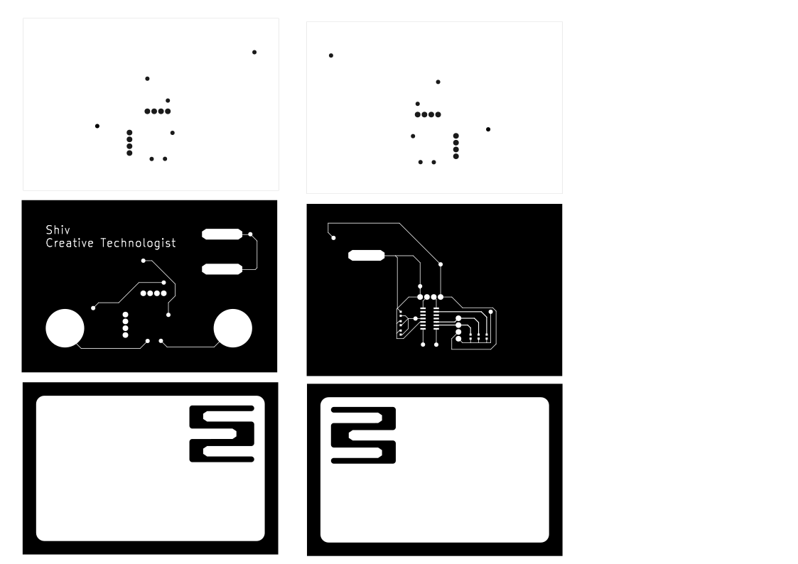
This week moved from designing circuits to physically making them. The pipeline: export from KiCad → process through modsproject.org → mill on the Roland SRM-20 → solder → test continuity → program over SWD → prove the chip is running. Every step has its own failure modes and most are irreversible once you've committed to copper.
The board is the interactive PCB business card I designed from scratch in Week 6, not a reference design. This week is its fabrication, programming, and testing: two failed two-sided mill attempts, a board snapped, a cut finger, a complete redesign to single-sided, and then firmware uploaded and nothing ran. All of it documented here because the failures are the content of the week. As part of the group assignment, we characterised the Roland's milling design rules, trace width, isolation, and tool choice, before cutting individual boards.
"Do the Z manually. Every time. The tool is fragile and the board is not flat."
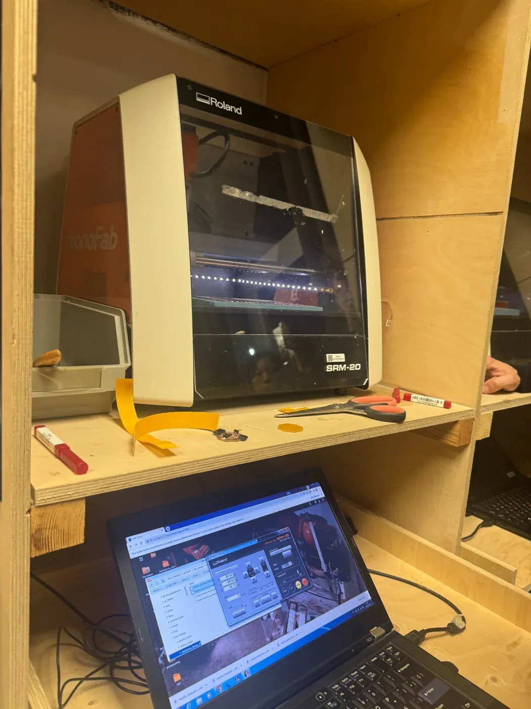
The Roland monoFab SRM-20. Yellow tape marks tool exposure before setting Z.
The Material: Cellulose PCB Stock (FR1)
The boards we mill are cellulose phenolic, known as FR1, a pressed paper-resin composite with a 0.1mm copper layer bonded to one side. Not fibreglass: FR1 uses cellulose paper, not the woven glass of FR4. It machines cleanly on the SRM-20 and produces fine dust, but that dust still irritates lungs and must never be handled bare-handed.
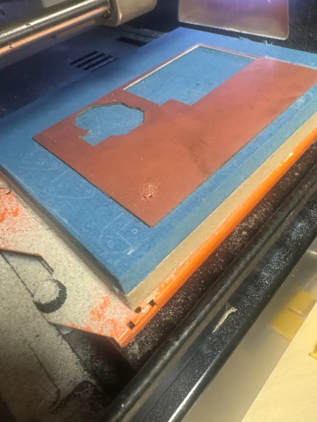
Cellulose FR1 PCB stock. The octagonal cutout shows a board already separated, different production method, same material.
Making the Toolpath: KiCad → Mods → .rml
The Roland SRM-20 doesn't read KiCad files. The
bridge is modsproject.org, a browser-based
node-graph CAM tool that converts image exports into
Roland-readable
.rml toolpath files. Three PNGs, three
operations.
Step 1: Export PNGs from KiCad at 1000 DPI
Polarity matters: getting it wrong means the mill cuts traces instead of isolation. Check in an image viewer before Mods, white should be copper. (For the group's line-test characterization we pushed resolution to 5000 DPI; at this board scale 1000 DPI from KiCad holds the trace detail without merging.)

Step 2: Mods Node Graph — V-bit Calculator
Programs → SRM-20 mill → mill 2D PCB loads a pre-wired node graph. I used a 30° V-bit with a 0.1mm tip rather than the standard 1/64" flat endmill. The V-bit calculator computes cut width from geometry: at 0.07mm depth with a 0.1mm tip at 30° → 0.1375mm cut width. Nearly 3× finer than the flat endmill, enough clearance to isolate fine-pitch pads.
Mods program selector. Think of it like nodes in Blender's shader editor, each block is a processing step, wired together to build the CAM pipeline.
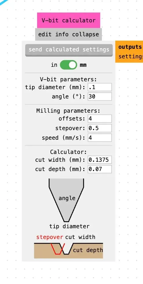
V-bit calculator: 0.1mm tip, 30°, 4 offsets, 0.5 stepover, 4mm/s. 0.07mm cut depth → 0.1375mm cut width, calculated automatically.
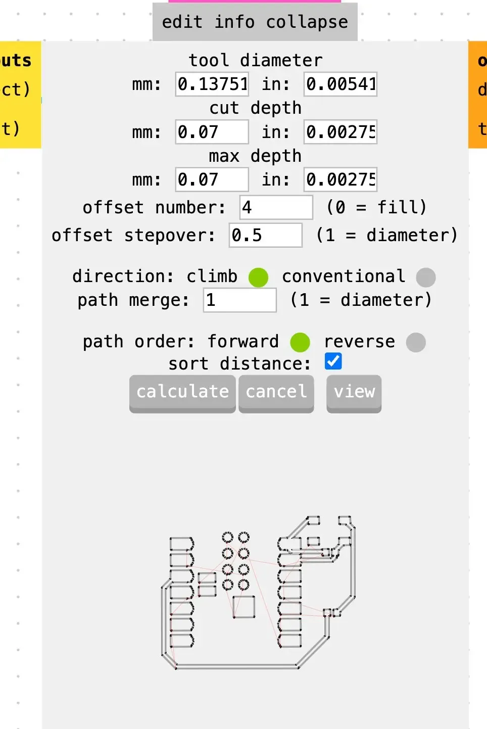
Mill raster 2D: tool diameter 0.13751mm, cut depth 0.07mm, climb direction. Toolpath preview confirms the isolation paths around each trace.
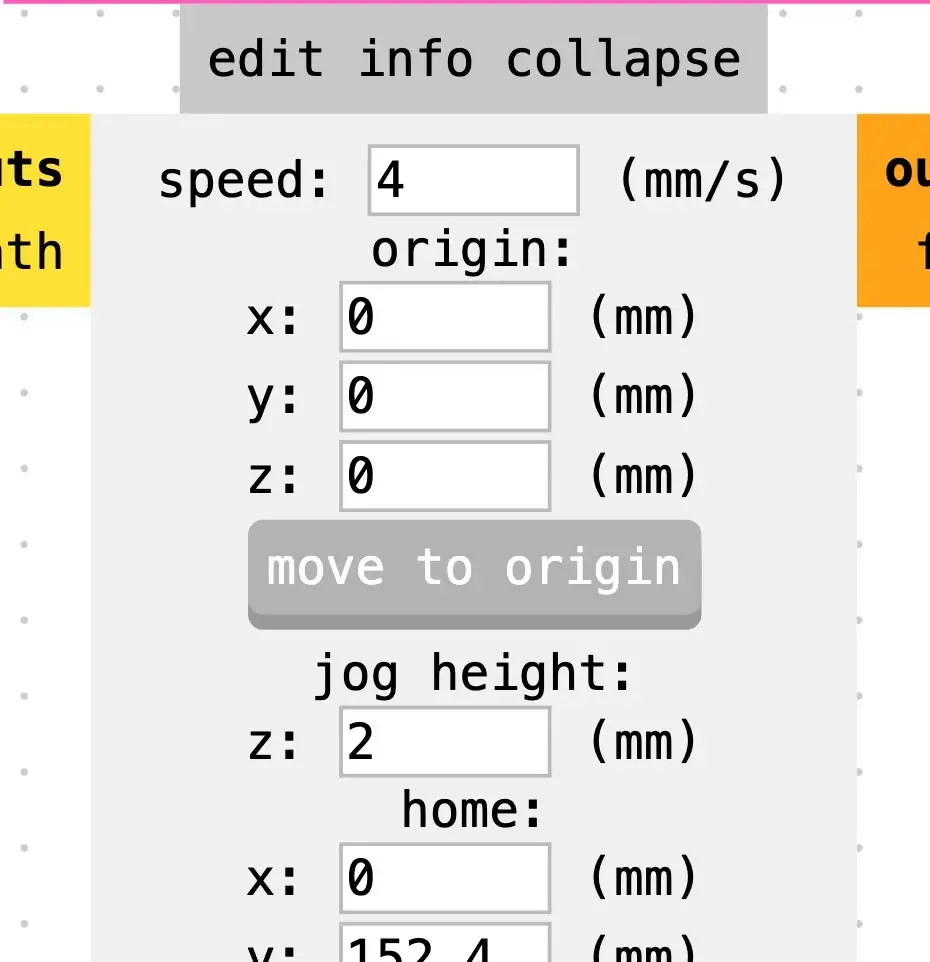
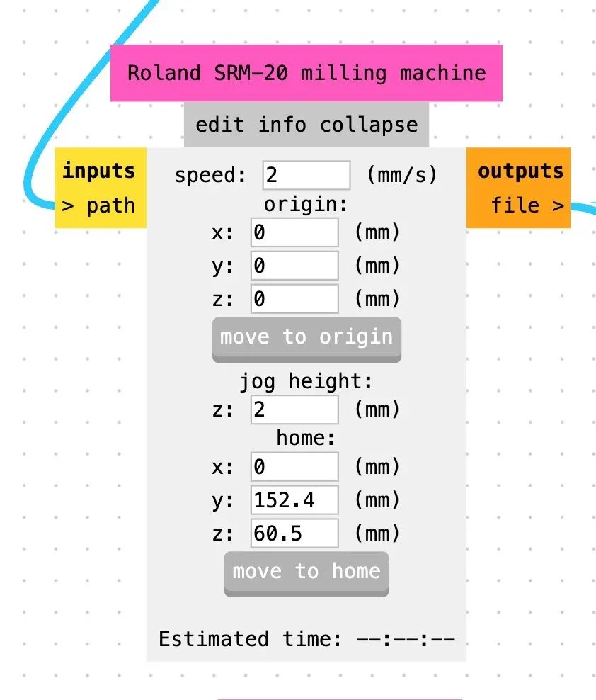
Roland SRM-20 node: 4mm/s, origin 0,0,0, jog height 2mm. The .rml file exports from the "file >" output and is sent directly to the machine.
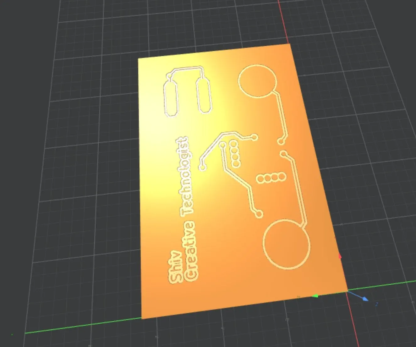
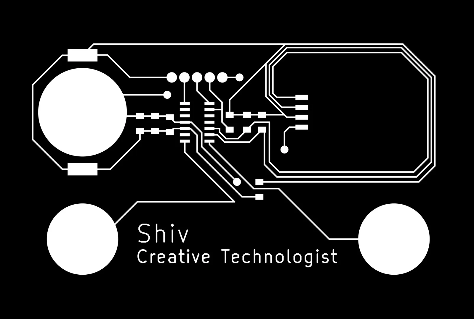
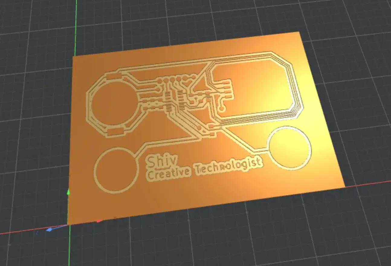
Toolpath simulation — front copper layer. "Shiv / Creative Technologist" visible, two capacitive touch circles, SWD pads. This is exactly what the mill will cut.
Milling
The copper layer is only 0.1mm deep. A 0.02mm Z error is the difference between a good trace and a broken one.
Z: Always Manual, Always Centre
Cellulose stock warps slightly, auto-zeroed Z at one corner will be wrong by the time the tool reaches the other. Fix: set Z manually at the board centre. This is the point closest to the average surface height and minimises maximum error across the full cut area. Set X and Y with the software, but Z is always manual, always last, always centre.
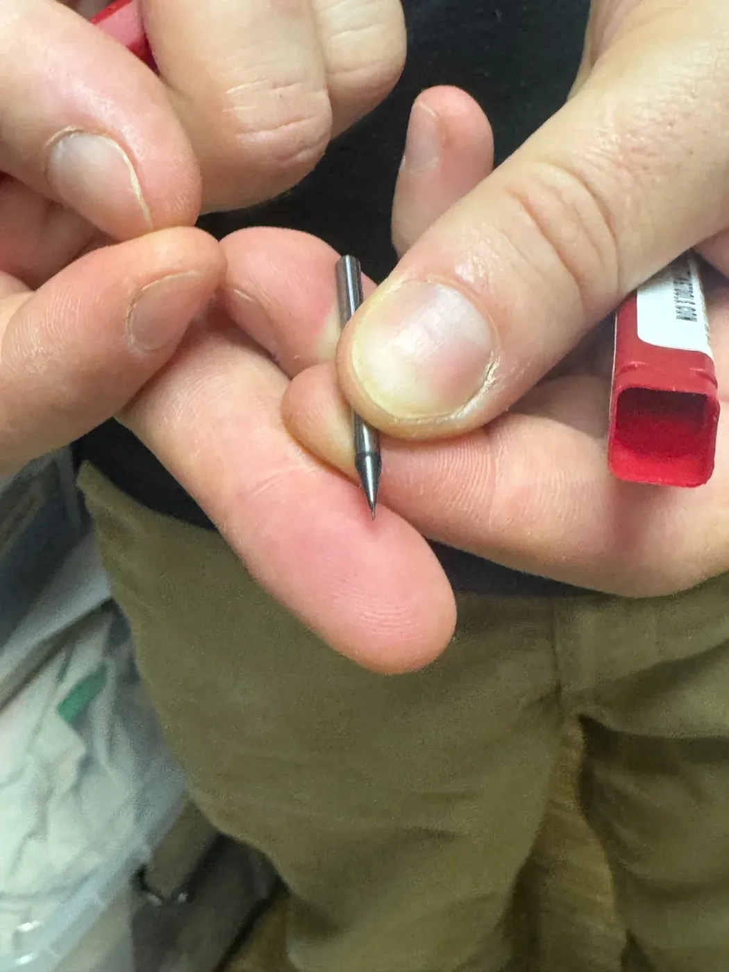
The V-bit. Any lateral force or a 0.05mm Z error and it snaps. Handle it like a needle.
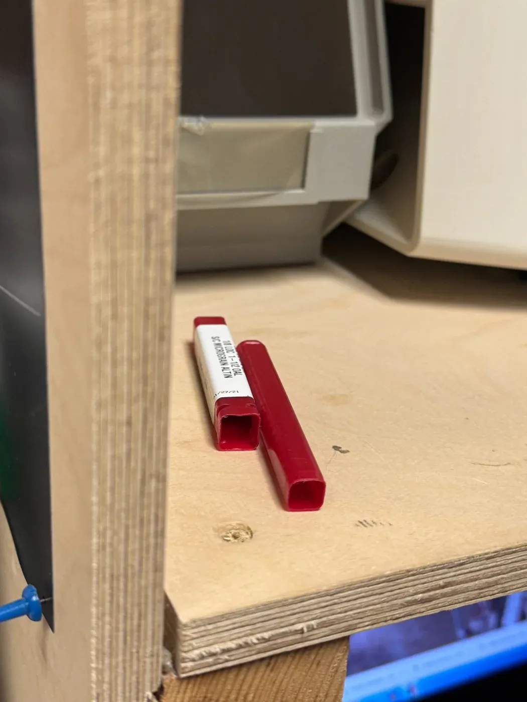
Bits live in their cases when not in the collet. The case is not optional.
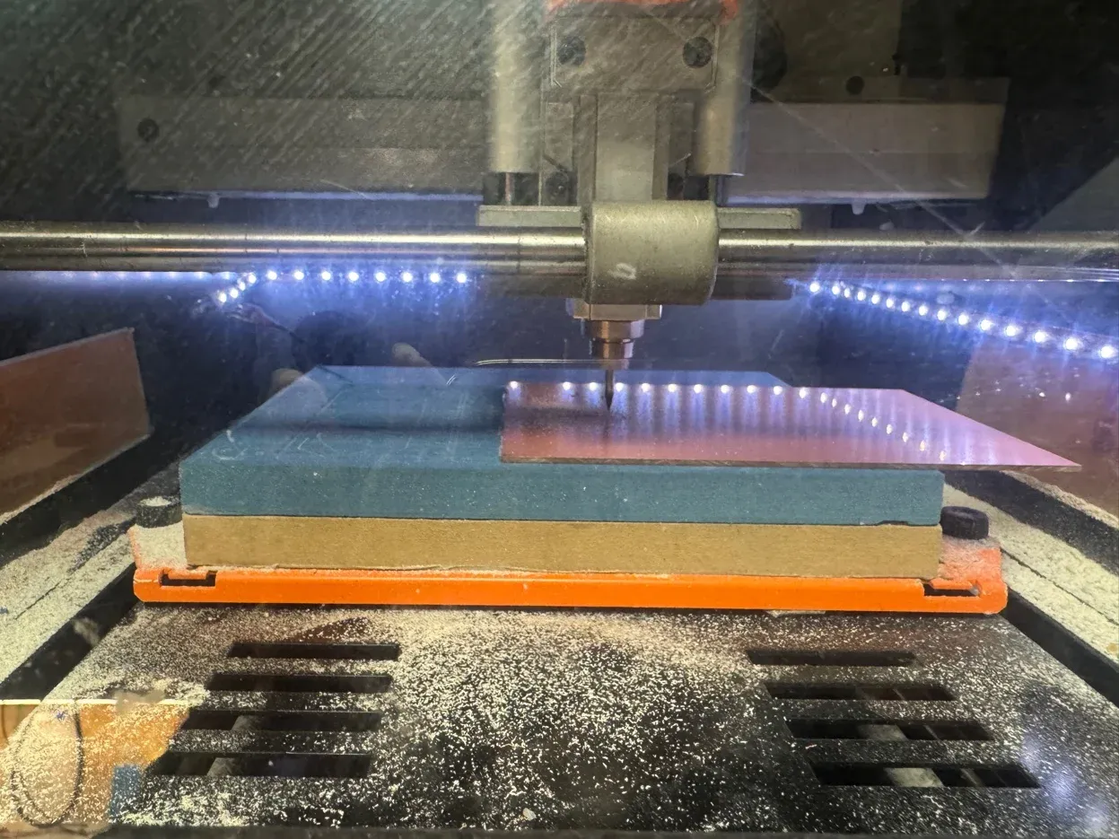
V-bit touching down on the cellulose stock. The blue layer is the sacrificial material. Copper dust forming around the tip.
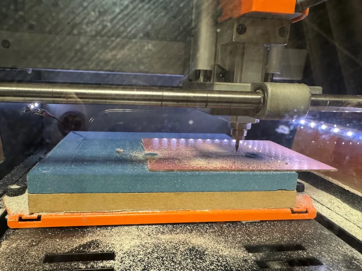
Side view mid-cut after the 50 micron Z adjustment. Isolation channels clean, grey grooves across the copper surface.
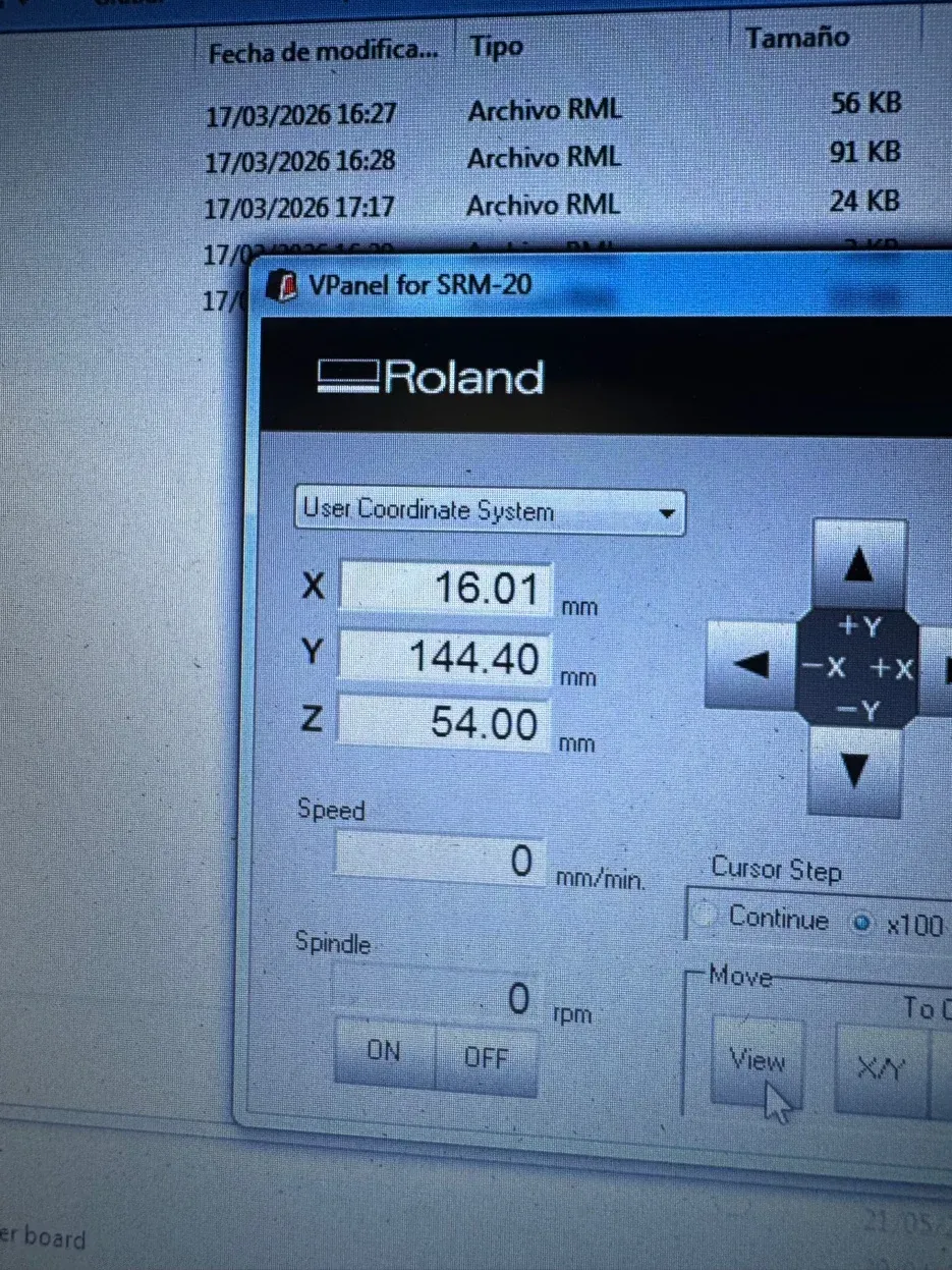
VPanel after zeroing. Each file in the sequence is a separate tool operation with its own Z re-zero.
My Board: PCB Business Card
Designed from scratch in Week 6 around the ATSAMD11C14A with capacitive touch pads, an SSD1315 OLED, and a CR2032 coin cell. "Shiv / Creative Technologist" etched directly into the copper, not silkscreen, because single-sided cellulose boards on the mill don't have a silkscreen layer. All traces on F.Cu.
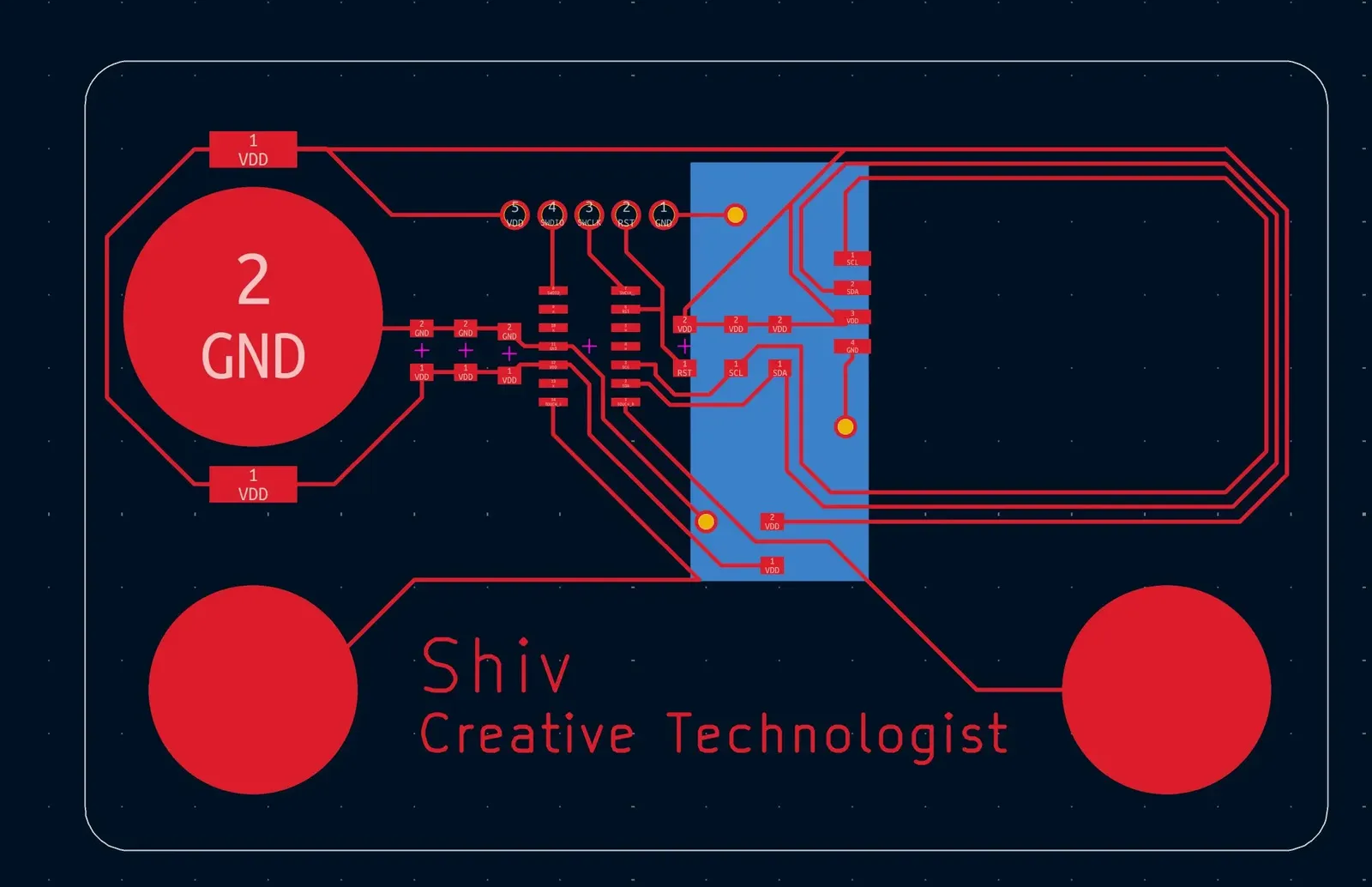
KiCad layout. The blue region is the OLED footprint over the microcontroller cluster. The two circles at bottom are capacitive touch pads; SWD header is the row of five pads top-centre.
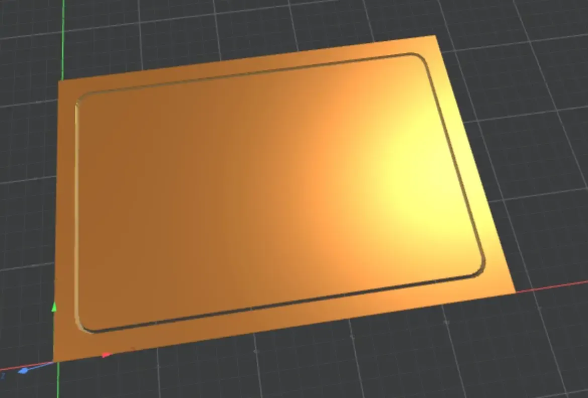
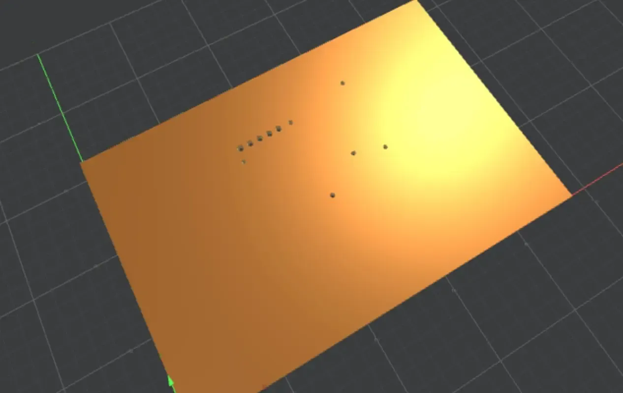
Two-Sided Failures → Single-Sided Redesign
Attempt 1: Front traces clean.
Wrong .rml file sent for the back,
wrong toolpath ran on a board that had taken
hours to reach that point. Scrapped.
Attempt 2: Fresh tape, fresh stock. Front traces clean. Tape lost adhesion during the flip, board shifted 0.3mm. Back traces completely misregistered. Scrapped.
Board handling: While removing the second failed board, the edge, sharp after the profile cut, cut a finger. Gloves for board removal, always.
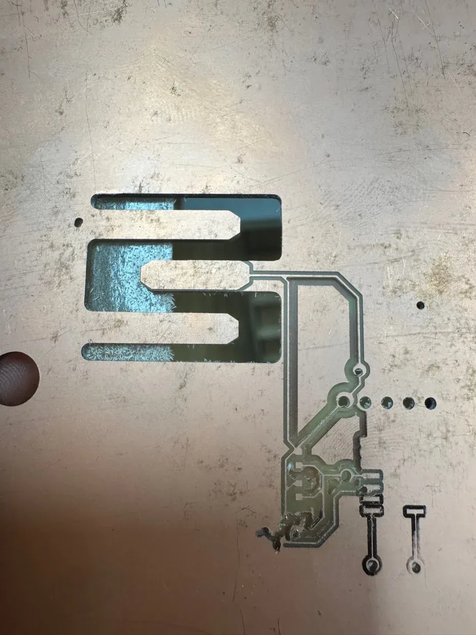
Failed flip: 0.3mm of drift when the tape let go. Back copper completely misregistered with the front.
Redesigned to single-sided with 0Ω resistor bridges where traces needed to cross, and a B.Cu copper pour as the ground plane. The spring-clip battery concept was scrapped, cellulose stock won't flex at business card dimensions, it snapped. Replaced with a Keystone 3034 CR2032 holder.
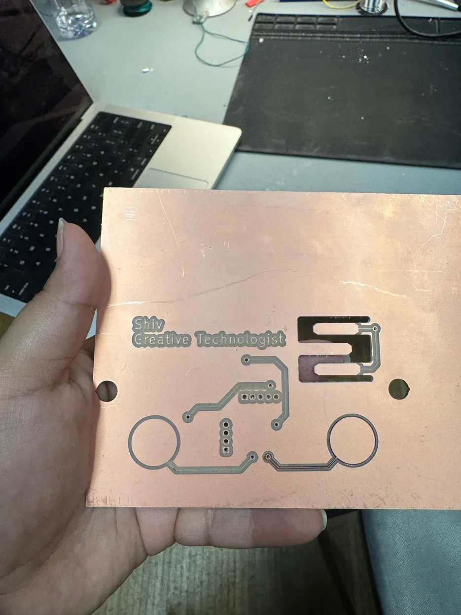
The milled front face. "Shiv / Creative Technologist" in copper, touch pad circles, SWD header pads. Alignment holes visible from the (failed) two-sided attempt.
Soldering & Continuity Testing
Soldering order: smallest and most heat-sensitive first. ATSAMD11C14A first, SOIC-14, 0.65mm pitch, flux-heavy drag soldering. Then 0402 passives and 0Ω bridges. Then OLED connector. Then CR2032 holder.
"Good solder joints are shiny. If it's dull or grainy, it's a cold joint, reheat it. Be quick, be rested, don't have coffee."
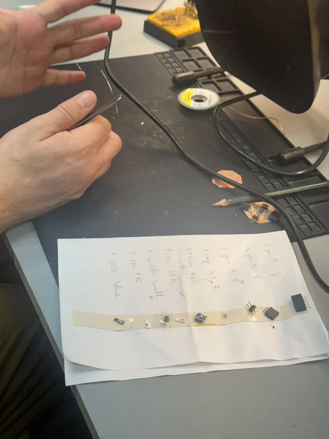
Components taped in assembly order, turns a stressful SMD session into a methodical one.
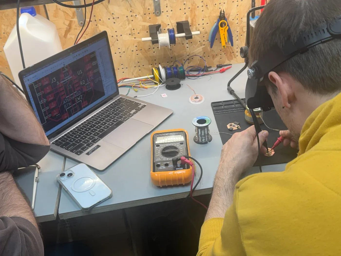
Full setup: KiCad layout open for reference, multimeter on continuity mode, solder reel, milled PCB on anti-static mat.
Continuity Testing, How the Board Is Proved Functional
After every component: multimeter in continuity mode. Each power rail probed end-to-end. Each ground via checked against the B.Cu plane. The two 0Ω bridges checked specifically, continuity across the bridge, no continuity to the trace running beneath. Any VDD-GND short caught here, before connecting power. Continuity passing on all critical paths is how the board is proved physically functional.
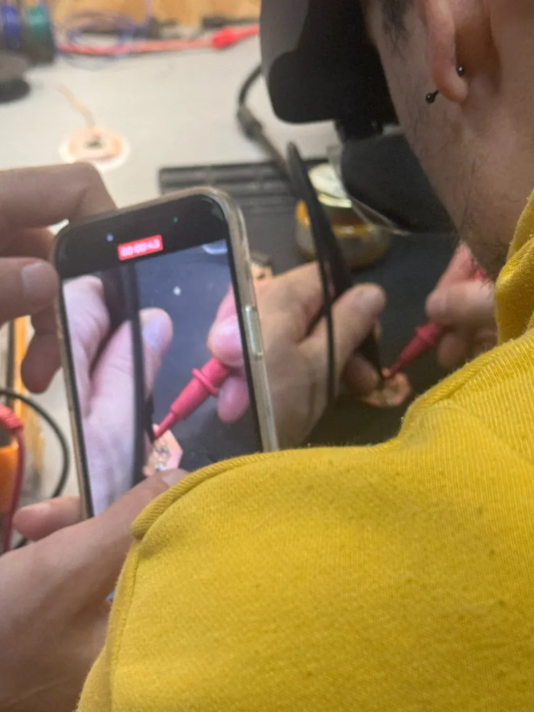
Phone camera as magnifier while probing, SMD pads are small enough that you can't reliably see bridges with the naked eye.
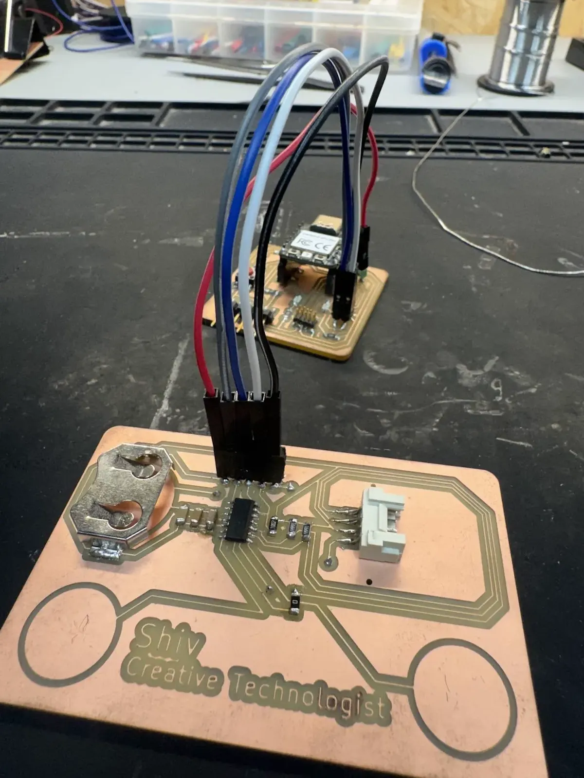
Board fully populated and connected to the Quentorres programmer. OLED socket right, CR2032 holder left. Continuity confirmed clean before connecting.
Programming — Proving the SAMD Runs
Upload succeeded. Nothing ran. No GPIO activity. The particular cruelty of embedded debugging: the tool says success and the board says nothing.
Root Cause: Wrong Flash Layout
Arduino Tools had
Bootloader Size → 4KB_BOOTLOADER
selected, firmware compiled to start at address
0x1000. But SWD programming via
Quentorres writes directly to flash from
0x0000. The chip powers on,
executes from 0x0000, finds
nothing, and hangs. The sketch at
0x1000 never runs.
The upload "succeeding" just means the SWD transfer completed. It says nothing about whether firmware landed in the right place.
Fix: Tools → Bootloader Size → NO_BOOTLOADER. Then Tools → Burn Bootloader, which despite the name sets fuses, clocks, and flash layout for direct SWD programming. After that, Sketch → Upload Using Programmer worked.
The Voltage Blinking Test, Proving the SAMD Is Running
No onboard LED, every pin is used for OLED, touch pads, or SWD header. To prove the chip was running after the flash layout fix, I uploaded a slow GPIO toggle and measured with a multimeter. Probe between GND and a GPIO pad. Expect 3.3V → 0V on a 5-second cycle.
void loop() {
  digitalWrite(PIN, HIGH);   // probe reads: 3.3V
  delay(5000);
  digitalWrite(PIN, LOW);    // probe reads: 0V
  delay(5000);
}
When the multimeter alternated between 3.3V and 0V on the 5-second cycle: chip confirmed running, board confirmed functional. 5 seconds is slow enough for a multimeter, no oscilloscope needed.
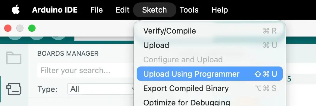
Sketch → Upload Using Programmer (⇧⌘U). Not the regular Upload, which assumes a serial bootloader. With NO_BOOTLOADER and SWD, this is the only path that works.
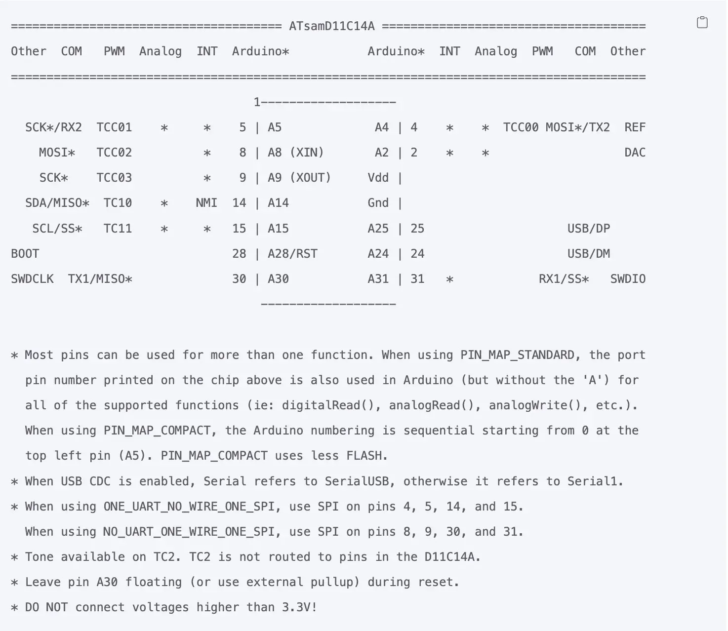
ATsamD11C14A pinout. SWDCLK pin 30, SWDIO pin 31. With PIN_MAP_STANDARD, Arduino number = physical pin number without the A.
Problems & Fixes
1. Z 50 microns too high, isolation too shallow
Stock warp meant channels weren't cutting through the copper. Fix: manually re-zero Z at board centre, increase depth by 50 microns, restart.
2. Wrong .rml file sent for back side
Machine ran the wrong toolpath on a board that had taken hours to get to that point. It does not ask for confirmation. Fix: numbered file prefixes + read filename out loud before every send.
3. Tape lost adhesion, board shifted 0.3mm during flip
0.3mm drift destroys layer registration. Fix: fresh tape every time, full surface coverage. Double-sided tape has one good stick.
4. Spring-clip battery snapped the board
Cellulose stock won't flex at business card dimensions. Fix: Keystone 3034 CR2032 through-hole holder.
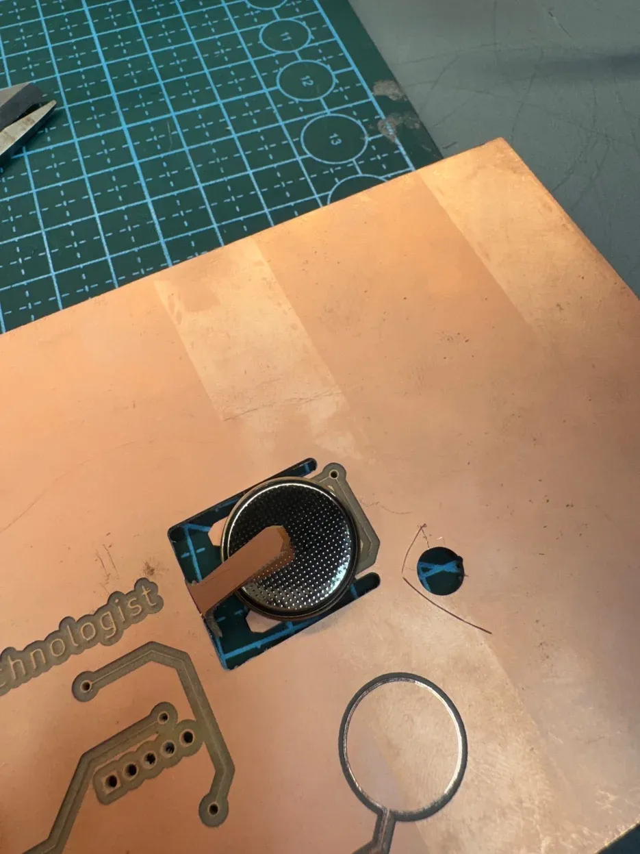
The milled pocket. No spring tension, material too stiff. Fix: proper holder.
5. Firmware uploaded, board silent, flash offset mismatch
4KB_BOOTLOADER placed firmware at
0x1000. Fix: NO_BOOTLOADER + Burn
Bootloader. Voltage blinking test confirmed fix.
Group Assignment: Characterizing the Mill & Going to a Board House
The group had two briefs: characterize our in-house PCB production process, and submit a PCB design to a board house. For the first, we ran a line test and compared three tools, the 1/64" flat end mill against 15° and 30° V-bits, measuring trace width, spacing, and resolution under a microscope. For the second, Max took his board out of the in-house mill workflow entirely and sent it off as Gerbers to a board house on the group's behalf. The full comparison, settings, captures, and manufacture write-up are on the group work page, linked in the sidebar.
The characterization result genuinely surprised me, and it's the part I keep thinking about. On paper the V-bit is the precise tool, a finer tip, a thinner cut, the obvious choice for tight isolation. In practice the group found the opposite: the V-bits were far more sensitive to setup, and the humble 1/64" end mill gave the more consistent, repeatable result. "More precise on paper" and "more reliable in the room" turned out to be two different things, and a tiny parameter like DPI or a few microns of Z could swing the whole outcome.
What makes this personal is that I went ahead and milled my own board with a 30° V-bit anyway, and lived exactly the fragility the group had measured. The shallow isolation, the re-zeroing, the snapped-tip anxiety: those weren't bad luck, they were the design rule the characterization had already told us about. The group work didn't just hand me numbers; it handed me a warning I then got to feel first-hand.
Watching the board-house route alongside my own in-house milling drew the contrast sharply. Milling, I own every variable, the Z, the tool, the kerf, and every failure is mine to fix. The fab route Max took is the mirror image: you hand the design off in a language someone else's machine reads, Gerbers and a drill file, not an .rml, plus a spec sheet of tolerances you trust them to hold. One process is total control and total fragility; the other is letting go and relying on a documented standard. Seeing both in the same week made that trade-off concrete in a way either one alone wouldn't have.
Design Files & Source Code
This board runs through four weeks: Week 6: Electronics Design → Week 8: Production (this page) → Week 9: Input Devices → Week 10: Output Devices. The editable KiCad project, the copper export, and the Mods milling toolpaths are below.
- visitingcardnew.kicad_sch — schematic (KiCad source)
- visitingcardnew.kicad_pcb — board layout (KiCad source)
- visitingcardnew.kicad_pro — KiCad project file
- visitingcard-F_Cu.svg — front copper layer export
- frontpath_png.rml — front traces toolpath
- backpath_png.rml — back traces toolpath
- frontvia_png.rml — vias toolpath
- frontcut_png.rml — outline cutout toolpath
- gpio_test.ino — voltage blinking test firmware