Overview
This week was about electronics design: going from zero knowledge of circuits to designing and milling a PCB in KiCad. We started with the absolute basics, what is a breadboard, how does Ohm's Law work, what do schematic symbols mean, and ended the week with a fully routed board ready for the Roland SRM-20.
Two tracks this week: first, learning the fundamentals by studying an ATtiny402 reference design and building a simple LED + button circuit from scratch. Then, applying everything to my actual project: an interactive PCB business card for ACM CHI 2026 in Barcelona, a coin-cell powered card built around an ATSAMD11C14A that detects when someone holds it with both hands, lights up an OLED with a random fun fact, and shares my website via NFC.
"A schematic and a PCB layout are two views of the same thing, one is the logical map, the other is the physical territory."
Electronics Fundamentals
Before touching KiCad, we started with the physical basics. Our instructor walked through Ohm's Law (V = I × R) and calculated the current for our LED circuit live on the projector: with a 5V supply and an LED forward voltage of ~2.2V, that leaves 2.8V across the resistor. At 2000Ω, that gives about 1.4mA, enough to light the LED without burning it out.
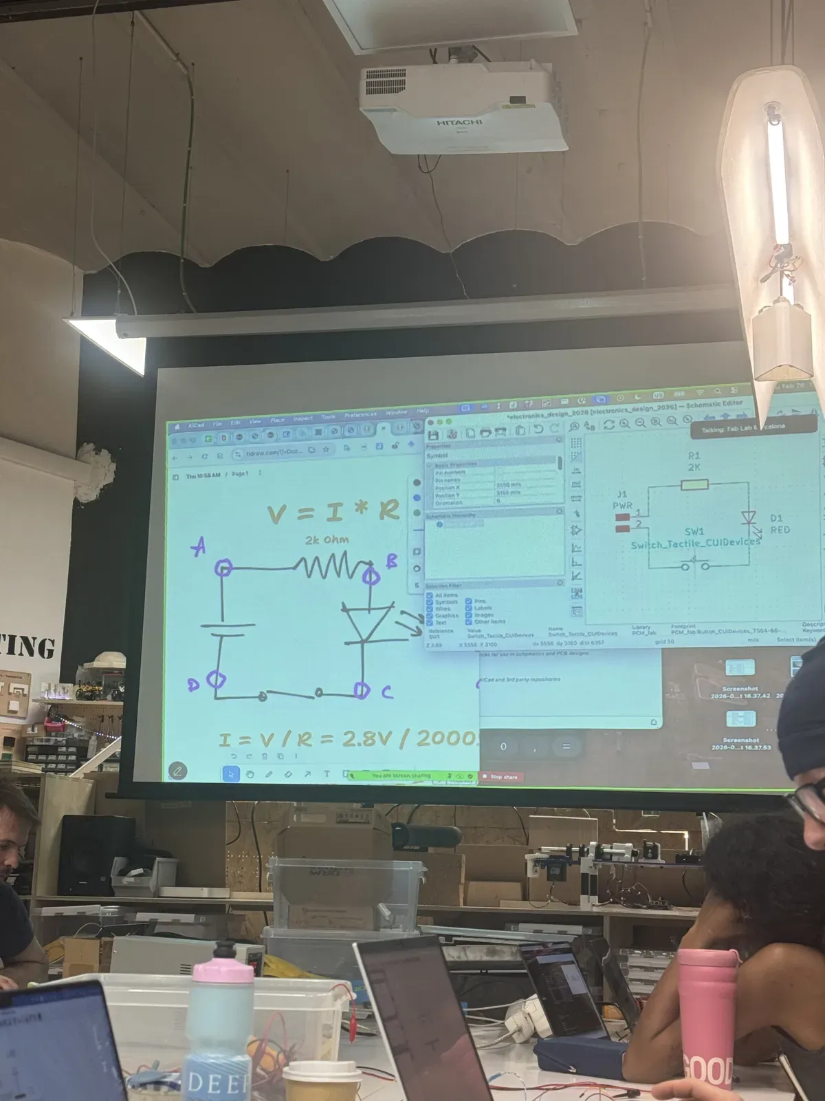
The class lecture, Ohm's Law (V = I × R) and the current calculation for our LED circuit: I = 2.8V / 2000Ω. On the right, the same circuit being built live in KiCad.
The Breadboard
A breadboard is a reusable canvas for prototyping circuits. The key insight: the holes are connected in specific patterns underneath. Each row of 5 holes on either side of the center gap is internally linked, plug a component leg into row 5 column A, and anything in columns B through E of row 5 is electrically connected to it. The center gap exists so you can straddle ICs across it, keeping each side of the chip on its own set of connections.
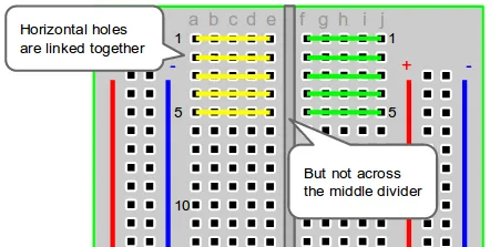
Horizontal holes in each row are linked together, but NOT across the middle divider. The long rails along the edges are for power (+) and ground (−).
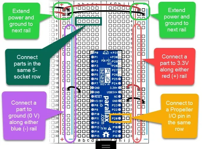
ICs sit across the center gap. Each pin gets its own row of 5 connection points. The red (+) and blue (−) power rails run the full length of the board.
First Hands-On: Breadboard Circuit
We gathered components, LEDs, a 2KΩ resistor, and a breadboard, and built the circuit we'd just calculated. This was the first time I'd assembled anything electronic from scratch: power in, resistor to limit current, button to control the circuit, LED to show it works.
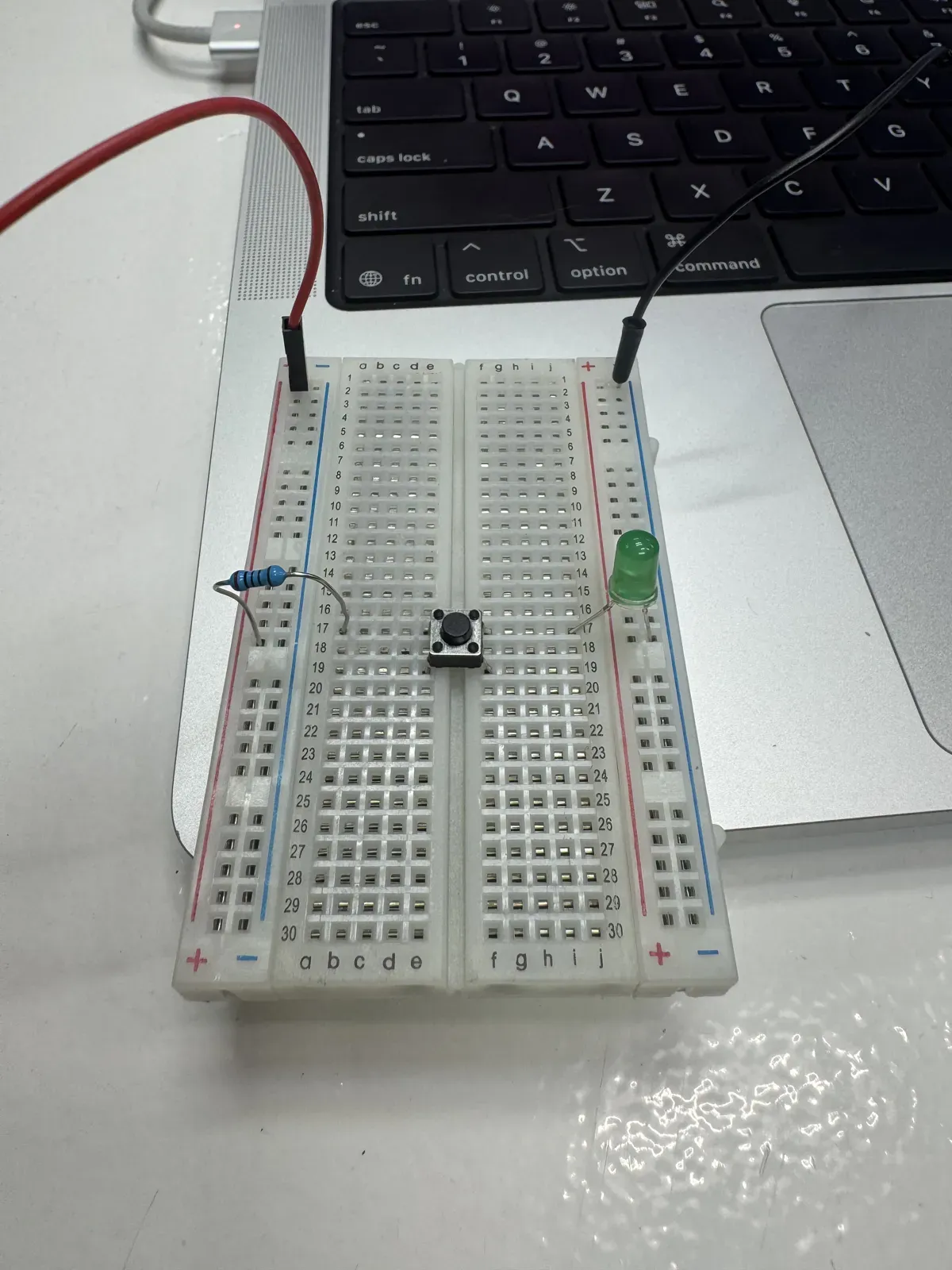
My first breadboard circuit! Resistor limits current, button controls the flow, green LED lights up. Powered from laptop USB.
Oscilloscope & Multimeter
We also got hands-on with oscilloscopes and multimeters. A multimeter tells you a single number (voltage, resistance, continuity). An oscilloscope shows you how a signal changes over time as a waveform, it's like the difference between checking someone's temperature once vs. watching their heart rate on a monitor.
Reading Schematics
A schematic is the blueprint of a circuit, it shows what components are used and how they're connected, without worrying about physical layout. Each component has a standardized symbol, and learning to read these is like learning a visual alphabet.
The most common symbols I needed this week:
- Resistors: zigzag lines that limit current flow (like a narrow section in a pipe slowing water down)
- Capacitors: two parallel lines that store and release energy (like a tiny rechargeable battery)
- Diodes/LEDs: triangles with a line; current flows in only one direction (one-way valve)
- Switches: a gap in a line that can be opened or closed
- Microcontrollers: rectangles with many labeled pins, the "brain" of the circuit
- VCC/GND symbols: power supply and ground reference, the "source" and "drain" of electricity
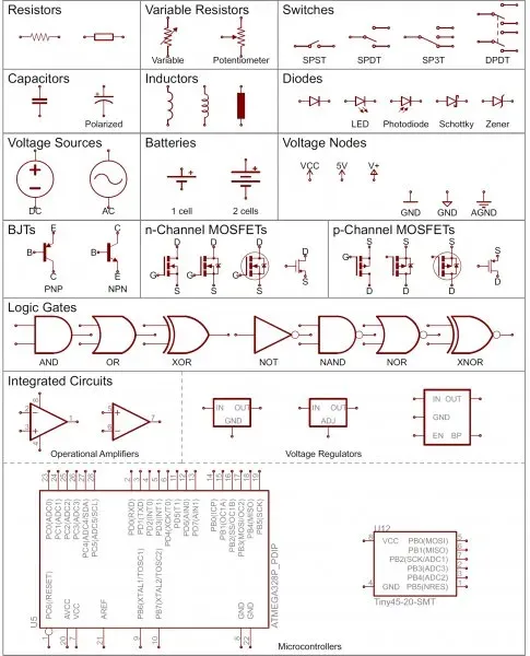
The visual alphabet of electronics, resistors, capacitors, diodes, transistors, logic gates, and integrated circuits all have standardized symbols.
Getting Started with KiCad
KiCad is the open-source EDA (Electronic Design Automation) tool we use at Fab Academy. The workflow has two main phases: first you draw the schematic (the logical connections), then you design the PCB layout (the physical board).
The first setup step was installing the FabLib library through KiCad's Plugin and Content Manager. FabLib is a component library built specifically for Fab Labs, it maps 1:1 with the parts available in the Fab Lab inventory, so when you pick a component in KiCad, you know it's physically available to solder. KiCad's symbol chooser shows both the schematic symbol (how it looks in your diagram) and the physical footprint (how it looks on the actual PCB), with links to each component's datasheet.
Understanding Datasheets
A datasheet is the manual for an electronic component. It tells you everything: what voltages it handles, how much current it draws, what each pin does, and how to wire it up. Reading datasheets felt intimidating at first, but the key sections to focus on are:
- Description: what the component actually does in plain terms
- Pinout: which pin is which (critical for not wiring things backwards)
- Absolute Maximum Ratings: the "don't exceed these or it dies" numbers
- Application Circuits: example wiring diagrams from the manufacturer
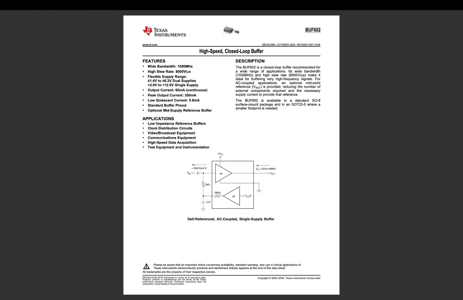
The BUF602 datasheet: we practiced reading through features, description, and the application circuit at the bottom. The application circuit is basically a "suggested wiring" from the manufacturer.
Studying the ATtiny402 Reference Design
Before designing my own board, we studied a reference design built around the ATtiny402 microcontroller. Our instructor broke PCB design into a 5-part checklist:
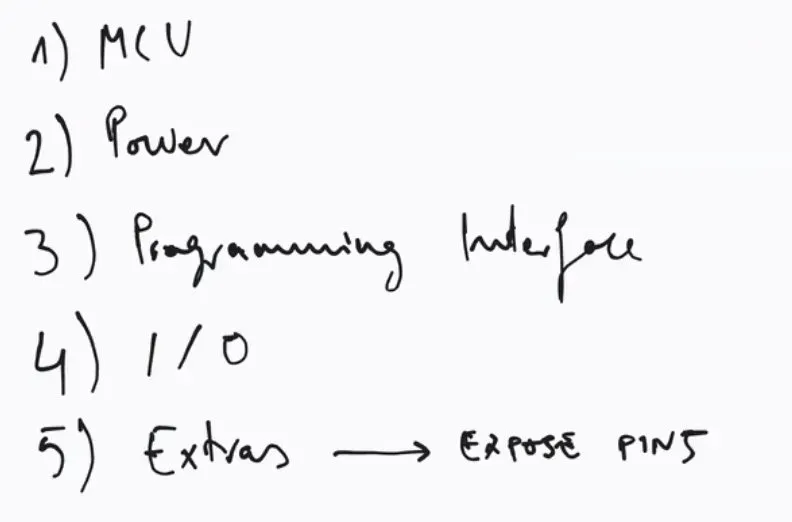
The PCB design checklist: every board needs these five things thought through.
The 5-Part Checklist
1. MCU (Microcontroller): the brain. The ATtiny402 is a tiny 8-pin chip running at 20MHz with 4KB of flash memory. 2. Power: how does the board get electricity? A 2-pin connector (J1) brings in 5V and GND, with a decoupling capacitor (C1) to smooth out voltage noise. 3. Programming Interface: how do you upload code? The ATtiny402 uses UPDI (Unified Program and Debug Interface), exposed through a 3-pin header (J2) with GND, UPDI, and 5V. 4. I/O (Input/Output): what does the board actually do? An LED with a current-limiting resistor (R1) and a push button with a pull-up resistor (R2). 5. Extras → Expose Pins: break out unused GPIO pins to a header (J3) so the board can be expanded later.
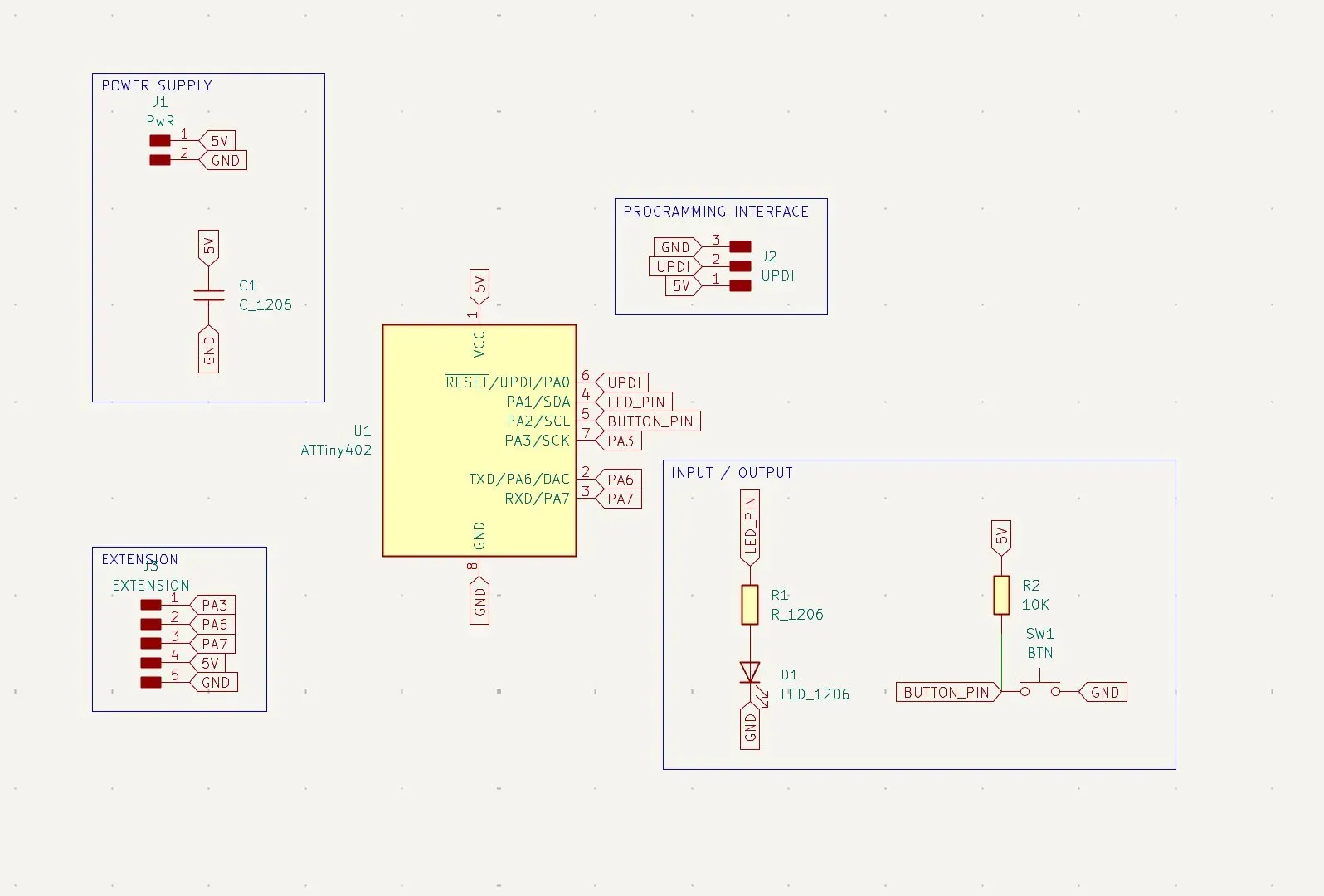
The complete ATtiny402 reference schematic: Power Supply (top left), Programming Interface (top right), MCU in center, I/O with LED and button (right), Extension connector (bottom left).
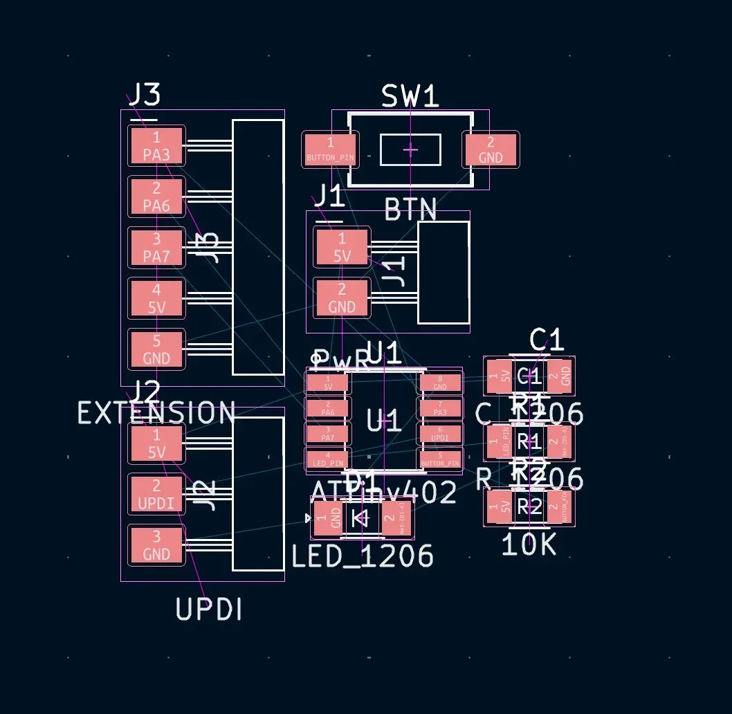
The same design as a PCB layout, the thin blue lines (ratsnest) show which pads need to be connected with copper traces.
My First PCB: LED + Button Circuit
To practice the full KiCad workflow, I designed a simple circuit from scratch: a power connector, a 2K resistor, a green LED, and a tactile button. The same circuit I'd already prototyped on the breadboard, now translated into a permanent PCB.
Schematic Design
I used PCM_fab (FabLib) components to ensure everything matched parts in the lab. The R_1206 resistor and LED_Luminus_1206 are surface-mount components in the 1206 package size, big enough to hand-solder but small enough for a compact board.
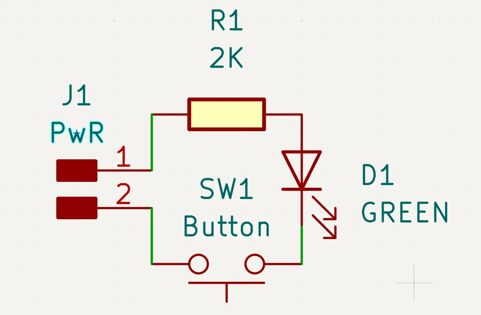
My schematic: power through J1 (PwR connector), R1 (2K resistor) limits current, D1 (green LED) lights up, SW1 (button) connects to ground.
Board Setup & Design Rules
Before laying out traces, you configure the board's design rules, manufacturing constraints like minimum trace width, clearance between traces, and via sizes. Think of it like setting minimum font size and margins before writing a document. Our settings: 0.4mm clearance, 0.3mm track width, 1.6mm via size, tuned for the Roland SRM-20 mill in our lab.
Routing the PCB
Routing is where you draw the copper traces that connect pads. KiCad shows the "ratsnest", thin lines indicating which pads need connecting, and you replace each one with an actual routed trace. The goal: zero unrouted connections.
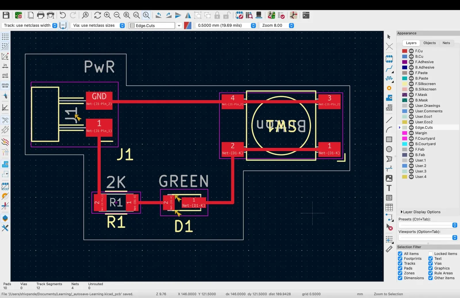
All connections made with copper traces (red). Status bar: 10 pads, 0 vias, 12 track segments, 4 nets, 0 unrouted.
Milling & Manufacturing
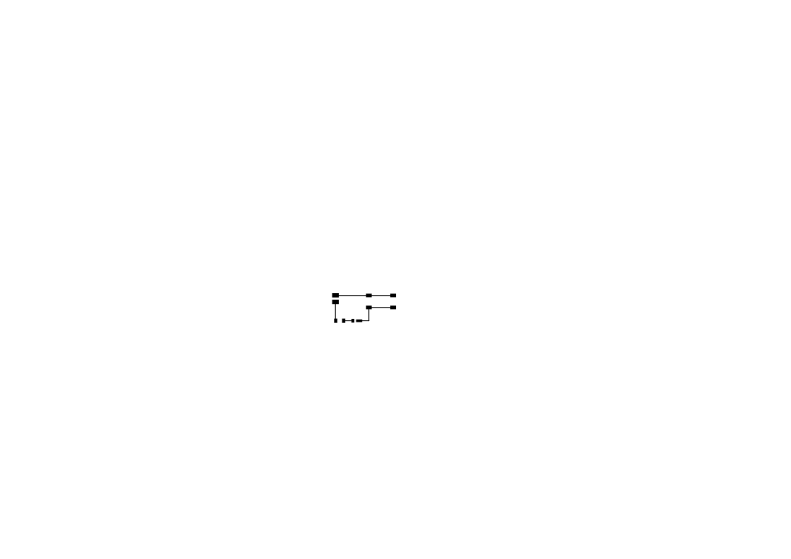
The final step is turning the digital design into a physical board. KiCad exports SVGs and Gerber files , one for the copper traces, another for the board outline, that the milling machine uses to carve the circuit.
Exported Files

The Roland SRM-20
We used the Roland SRM-20 desktop milling machine to cut the board. The process starts with a blank copper-clad FR1 board, a thin sheet of copper bonded to a phenolic substrate. The mill carves away copper to leave behind the circuit traces.
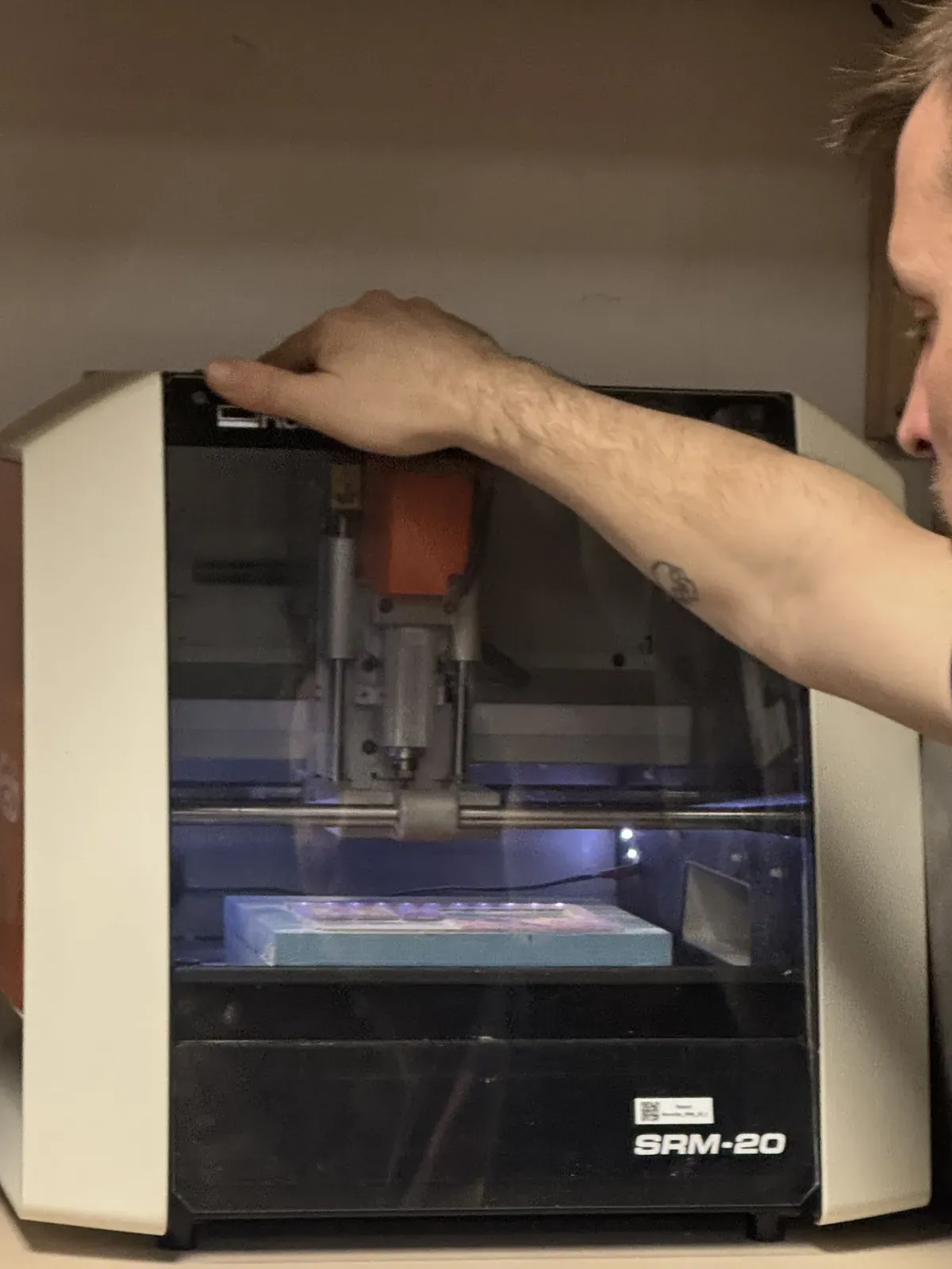
The Roland SRM-20, a tiny CNC machine that carves away copper to leave behind circuit traces.
My Project: Interactive PCB Business Card
With the fundamentals down, I designed something I'd actually use: an interactive PCB business card for ACM CHI 2026 (the premier conference on Human-Computer Interaction, happening in Barcelona this year). The idea: a self-contained electronic card that you hand to someone. When they hold it with both hands, their fingers touch capacitive pads, which triggers an OLED screen to display a random fun fact about me. They can also tap the card with their phone to open my website via NFC. No buttons, no instructions, the interaction is the interface.
"The best business card is one that makes someone stop and hold it with both hands."
The Concept
The card is powered by a CR2032 coin cell battery, held in place by the tension of the PCB itself rather than a traditional battery holder, the board acts as a spring clip. At the center is an ATSAMD11C14A microcontroller, which controls the interaction. Two large circular copper pads on the left and right edges serve as capacitive touch sensors. When both pads are touched simultaneously (i.e., someone holds the card with two hands), the MCU wakes up and drives a small OLED display over I2C to show a random fact. A passive NFC tag sits in a copper-free zone of the PCB, so tapping a phone to the card opens my website.
Schematic Design
Applying the 5-part checklist from the ATtiny402 lesson to a more complex design:
1. MCU: The ATSAMD11C14A, a 14-pin ARM Cortex-M0+ running at 48MHz with 16KB flash. Much more capable than the ATtiny402, which I needed for driving the OLED display and handling capacitive touch sensing. 2. Power: A CR2032 coin cell (3V) with three decoupling capacitors: C1 (0.1µF) for high-frequency noise, C2 (1µF) for mid-range, and C3 (10µF) as a bulk cap for the OLED's current spikes. 3. Programming Interface: A 4-pin SWD header (J2) with VDD, SWDIO, SWCLK, and GND, the ARM equivalent of UPDI. 4. I/O: Two capacitive touch pads (TOUCH_L on PA04, TOUCH_R on PA05), an I2C OLED display (J1 with VDD, GND, SDA, SCL), and a passive NFC antenna. 5. Extras: I2C pull-up resistors R2 and R3 (4.7KΩ each) on SDA and SCL, and a 10KΩ pull-up on the reset line (R1).
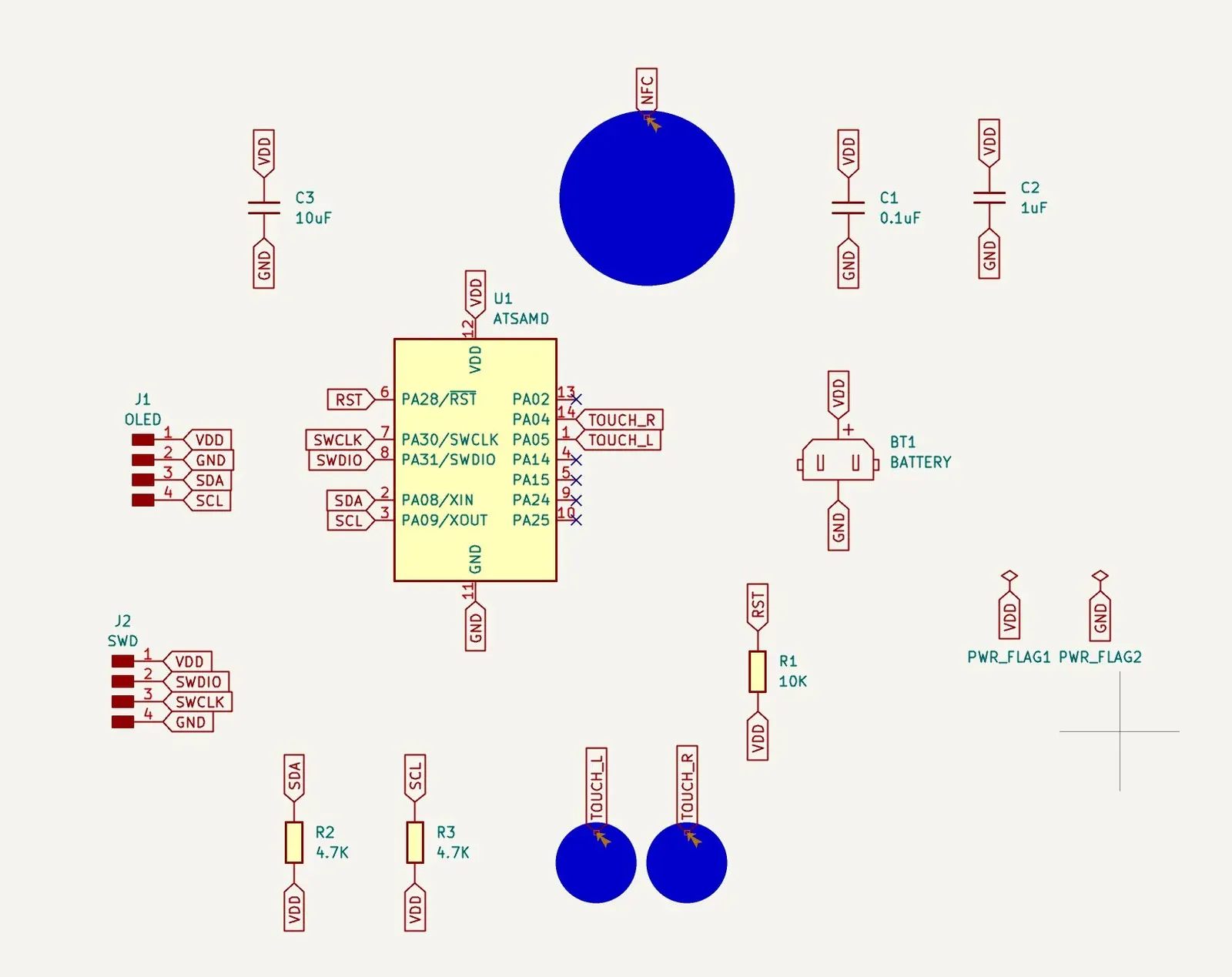
The full schematic, ATSAMD11C14A at center, OLED connector (J1) on the left, SWD header (J2) below, CR2032 battery on the right, capacitive touch pads at the bottom, NFC antenna up top, and three decoupling caps for clean power.
Prototyping the Interaction
Before committing to the PCB, I prototyped the core interaction on a breadboard using the Barduino (ESP32-S3) as a stand-in for the ATSAMD. The Barduino's touch-capable GPIO pins let me test the capacitive sensing logic, and I wired up the OLED display over I2C to validate that the "hold with two hands → screen lights up" flow actually felt right. Same principle as the simple LED circuit earlier, prove it works on a breadboard before you route it in copper.
The Barduino wired to the OLED on a breadboard, testing I2C communication and the capacitive touch interaction before designing the final PCB.
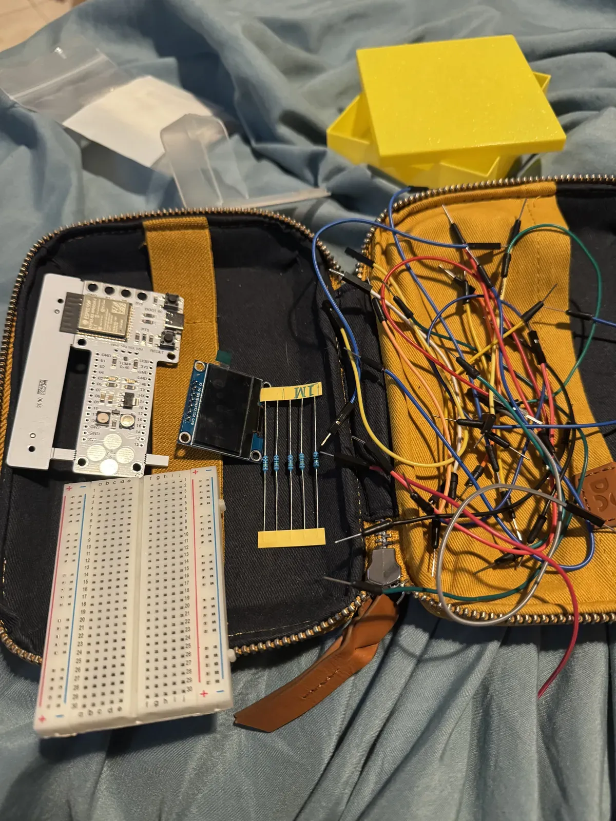
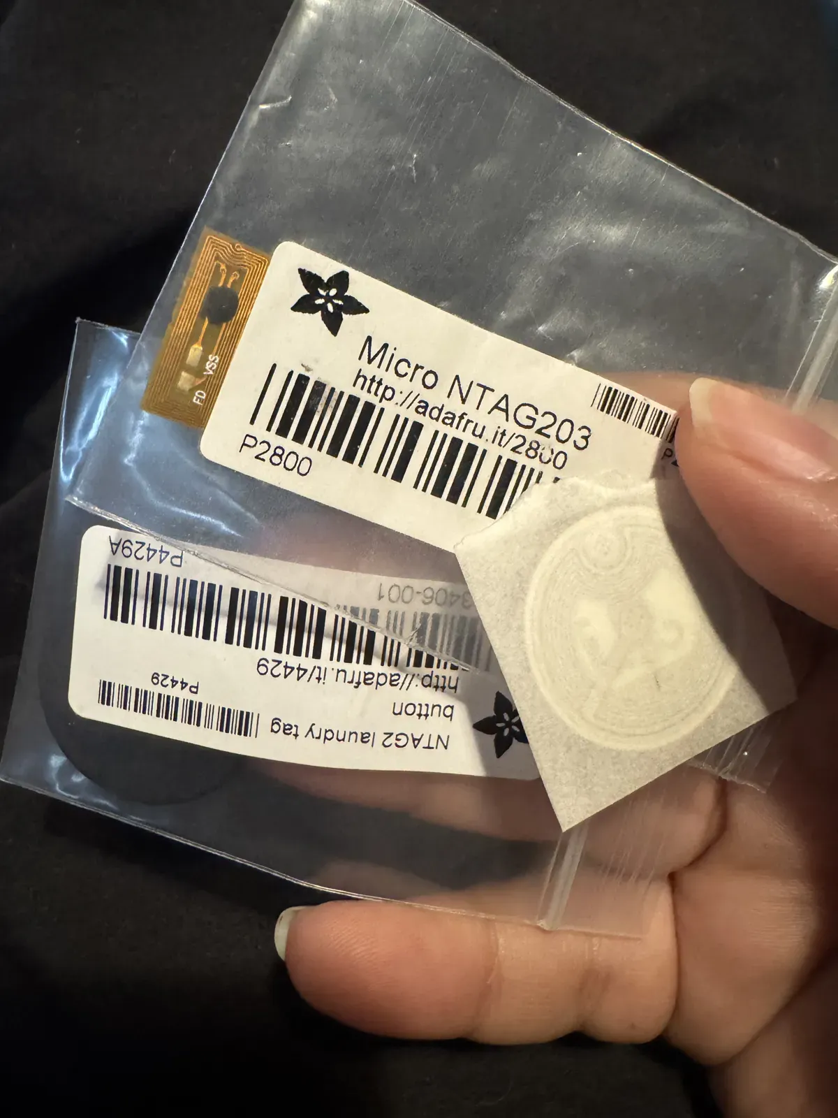
The full prototyping kit, Barduino, OLED, breadboard, resistors, jumper wires, and the different NFC tag types I explored for the business card.
PCB Layout
The layout is designed to look like a business card. "Shiv / Creative Technologist" is silkscreened in the top-left corner. The two large circular copper pads sit at the left and right edges, positioned exactly where your thumbs naturally land when you hold a card-sized object. The CR2032 holder is in the top-right, with the battery sandwiched between the PCB and a GND pad using board flex as a spring clip. The NFC tag gets a copper-free keepout zone so the antenna isn't shielded by the ground plane. The OLED sits on the left edge, and all the dense SMD components (MCU, resistors, caps) cluster in the center.
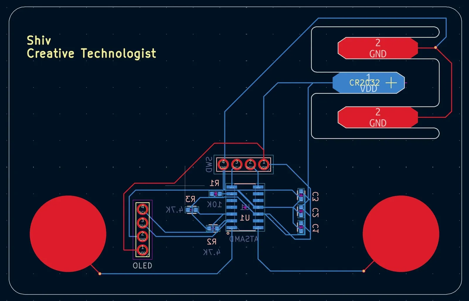
The PCB layout, red traces on the front copper layer, blue on the back. The two large red circles are the capacitive touch pads. CR2032 battery holder top-right, OLED connector left edge, ATSAMD and passives clustered in the center.
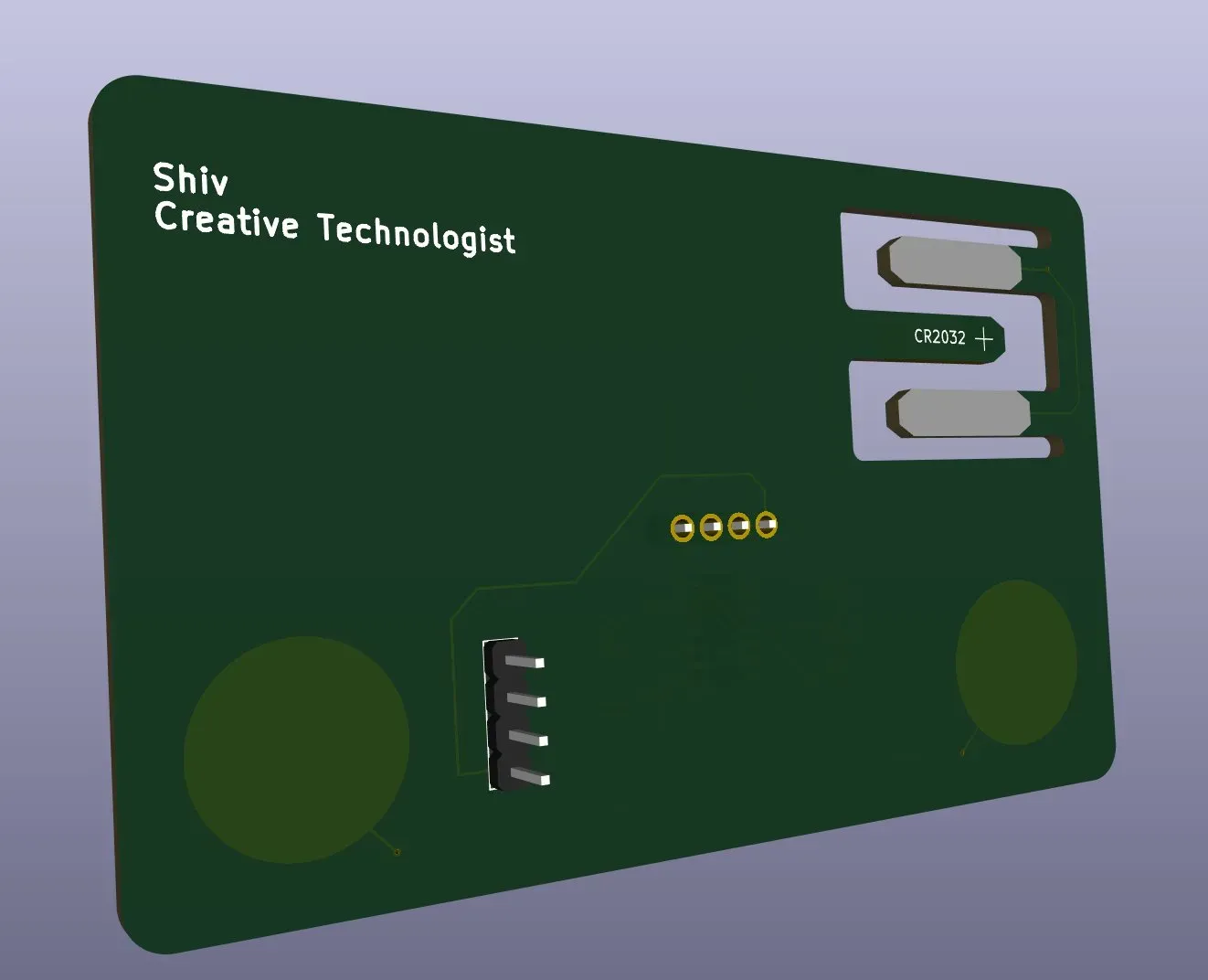
3D render, front, "Shiv / Creative Technologist" silkscreened in the corner, capacitive touch pads on each side, CR2032 spring-clip battery holder top-right, OLED and SWD headers visible.
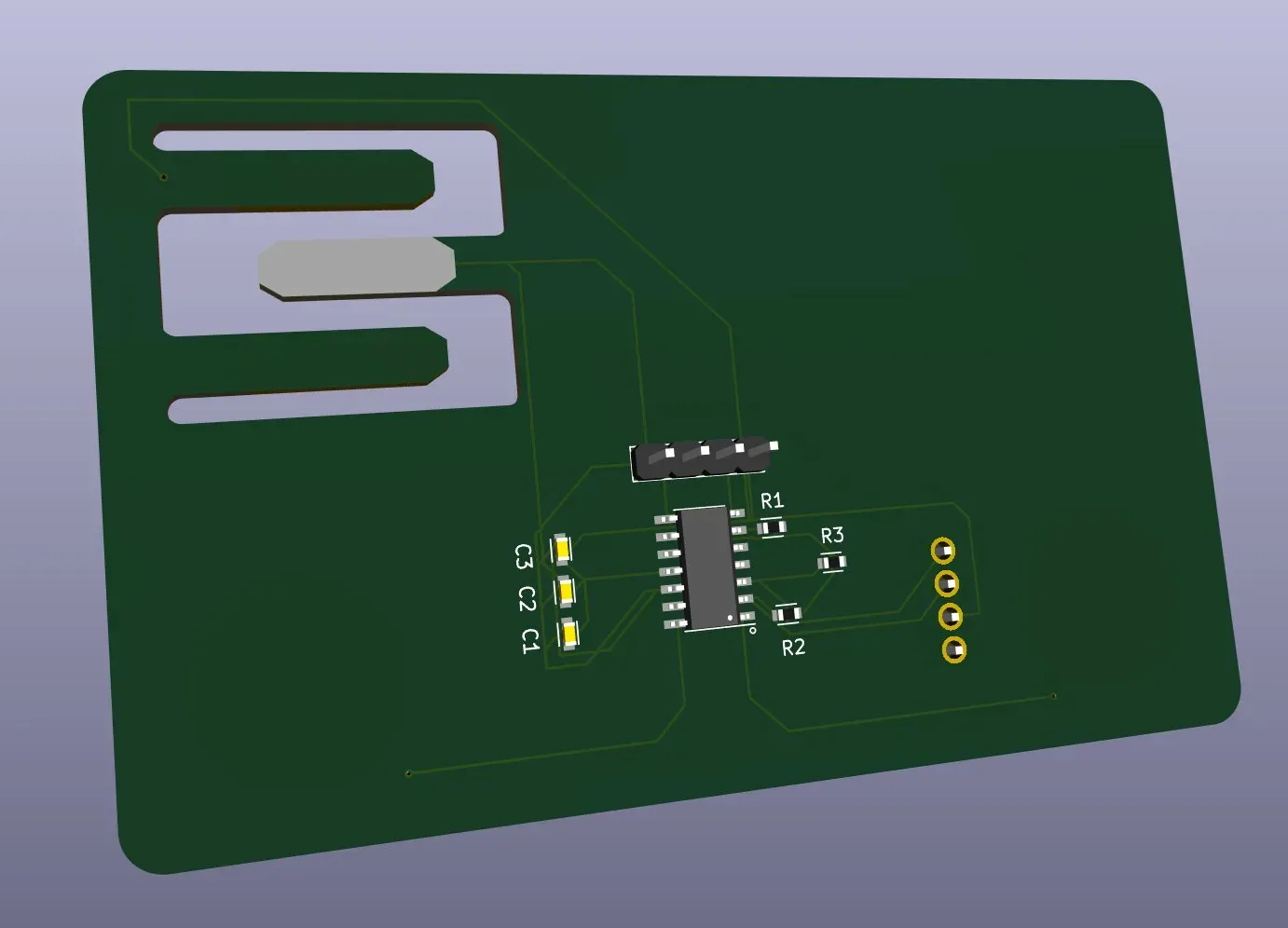
3D render, back, the ATSAMD11C14A and all the passives (C1, C2, C3, R1, R2, R3) clustered in the lower half, with the CR2032 pads and SWD programming header visible.
Design Revision: Single-Sided for Production
After two failed two-sided mill attempts in Week 8, the board was redesigned to be single-sided wherever possible. Three specific changes made this work:
- 0Ω resistor bridge: One trace couldn't be routed without crossing another on a single layer. Rather than using a via (which requires a second copper layer), a 0Ω resistor acts as a physical jumper, it's a real component that costs nothing and routes the signal across the conflicting trace. Common single-sided trick.
- Ground plane on back copper: All GND connections are tied to a solid copper pour on the B.Cu layer rather than individual traces. This simplifies routing significantly, any component needing ground just drops a via to the pour, and also improves noise immunity and heat distribution. The back copper is now essentially one big ground plane rather than a second routing layer.
- Battery holder footprint: The spring-clip battery concept was removed after proving unworkable in the 1.6mm milled FR1 cellulose stock (see Week 8), it snapped rather than flexed. Replaced with a proper CR2032 through-hole holder, more height but actually retains the battery.
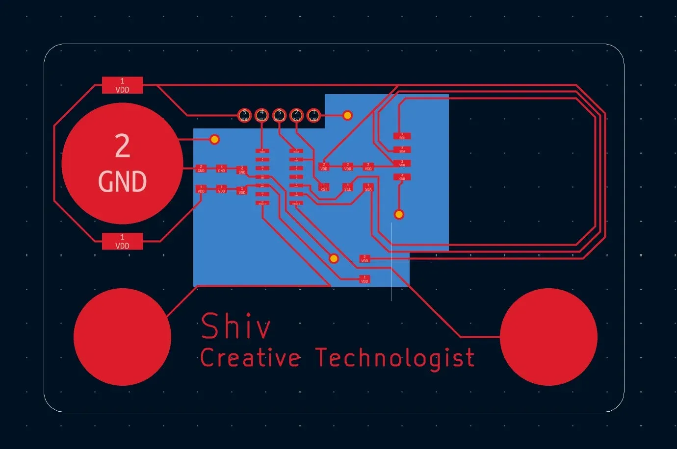
Revised layout: red = F.Cu front traces, blue = B.Cu ground plane fill. All signal routing is now on the front layer. The 0Ω resistor bridge handles the one crossover that couldn't be resolved on a single layer. Touch pad circles and silkscreen unchanged.
Before sending anything out, I checked that the board could actually be fabricated. KiCad's Design Rules Check (DRC) came back with zero clearance or trace-width violations, and the single-sided routing plus the 0Ω bridge keeps every signal millable on the SRM-20, 0.4mm clearance and a 0.3mm minimum trace, comfortably within what the V-bit can isolate. Passing DRC against the fab's constraints is what tells you a layout is truly fabricable, not just visually finished.
This version was submitted to JLCPCB for factory fabrication and will be soldered and tested in Week 10 and Week 11.
Design Decisions
A few things I had to think through that weren't covered in the simple LED circuit:
- Two-layer board: The business card uses both F.Cu (front copper) and B.Cu (back copper) for routing, the simple LED circuit was single-sided. This means I need vias to jump between layers, but it gives much more routing freedom on a tight board.
- Capacitive touch sizing: The touch pads need to be large enough to reliably detect a finger through skin contact. The large circular pads maximize surface area for consistent capacitive sensing.
- NFC keepout: The NFC tag is passive (no power needed), but copper near the antenna would shield the magnetic field and prevent phone detection. So the NFC area has no copper pour.
- Battery as spring clip: Instead of a traditional battery holder (which would add height and cost), the CR2032 is sandwiched between two PCB pads with the board's flex providing retention force. Elegant but requires careful pad geometry.
- Power budget: A CR2032 has about 220mAh. The card sleeps until both touch pads are activated, so standby draw is minimal. The OLED only runs during interaction.
Group Assignment: Observing an MCU with a Logic Analyzer
The brief was to use the lab's test equipment to observe how an embedded microcontroller actually behaves. We watched a Barduino drive a set of stepper motors through ULN2003 drivers, and to see what the chip was really doing we put a logic analyzer on its control pins. The full rig, wiring, and captures live on the group work page, linked in the sidebar, what I want to reflect on here is what it changed about how I think.
The thing that stayed with me is how much of a microcontroller's work is simply invisible. A motor spins, an LED blinks, and it's tempting to treat the chip as a black box that either works or doesn't. The logic analyzer collapsed that mystery into something I could read: the signals weren't random, they were a sequence, coils firing one after another in a steady, phase-shifted rhythm, each pulse a decision the code had made. Seeing the line between software I wrote and electricity moving made the two feel like one continuous thing rather than two separate worlds.
That reframed debugging for me. Up to this week, when something electronic didn't work I'd guess and swap parts. Watching the group instrument a live circuit taught me there's almost always a way to look instead of guess, and that's the instinct I'm carrying into my own business-card board, where the I2C lines between the MCU and the OLED are exactly the kind of invisible conversation a logic analyzer would let me see.