Electronics Production
Overview of week 8
Group Assignment
- Characterize the design rules for our in-house PCB production process: document feeds, speeds, plunge rate, depth of cut (traces and outline) and tooling.
- Document the workflow for sending a PCB to a boardhouse
Individual Assignment
- Make and test a microcontroller development board that we designed
Group Assignment :
Exported the PCB design in SVG format and generated G-code using MODS software for 2D milling.
Set tool parameters using a 1/64 inch V-bit (30°), calculated depth with a V-bit calculator, and prepared the milling machine.
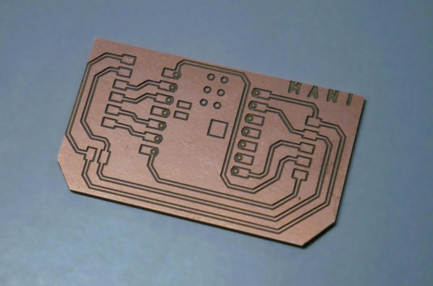
Initial milling failed due to excessive depth; adjusted parameters multiple times for improved results, after that I understand the tool depth setting and conclude the final PCB production.
Individual Assignment :
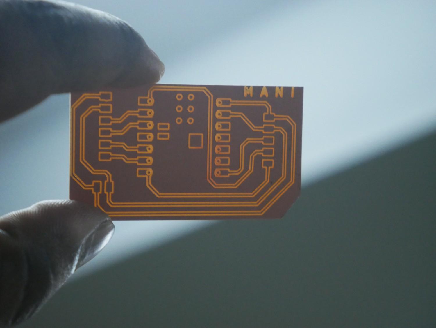
Hero shot
PCB (Printed Circuit Board)
A Printed Circuit Board (PCB) is a flat board made of insulating material with conductive pathways etched onto its surface to connect electronic components. It provides mechanical support and electrical connections for integrated circuits, resistors, capacitors, and other elements. PCBs come in various types, including single-layer, double-layer, and multi-layer designs, depending on complexity. They are manufactured using etching, drilling, and soldering processes. Design and fabrication require software tools like Altium Designer, KiCad, or Eagle.
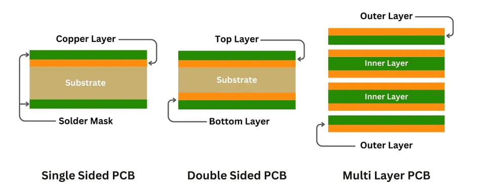
Single Layer PCB
A Single Layer PCB has a single conductive copper layer on one side of an insulating substrate. It is the simplest and most cost-effective PCB type, commonly used in low-complexity electronic circuits. Components are mounted on one side, while the copper traces for connections are on the other. These PCBs are easy to design, manufacture, and repair, making them ideal for basic applications like LED circuits, calculators, and power supplies. They have limitations in handling complex circuits due to restricted routing space. Materials like FR4, phenolic resin, or CEM-1 are used for their construction.
Double-Layer PCB
A Double-Layer PCB has conductive copper layers on both sides of an insulating substrate, allowing more complex circuit designs. It features vias (plated holes) to connect components between layers, improving circuit density and functionality. These PCBs are commonly used in industrial controls, power supplies, and automotive electronics. Compared to single-layer PCBs, they offer better electrical performance and routing flexibility while remaining cost-effective. Materials like FR4, CEM-3, and polyimide are used for durability and reliability. Design tools such as Altium Designer, KiCad, and Eagle help in layout and manufacturing preparation.
Multi-layer PCB
A Multi-Layer PCB consists of three or more conductive copper layers stacked with insulating layers in between. It enhances circuit complexity, allowing higher density and reduced size. Vias (through-hole, blind, and buried) connect different layers for efficient signal routing. These PCBs are used in high-performance electronics like medical devices, aerospace systems, and advanced computing.
Common materials include FR4, polyimide, and PTFE (Teflon) for thermal stability.
PCB Fabrication
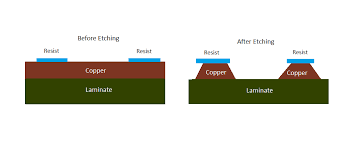
Etching
Etching is the process of removing unwanted copper from a PCB to create conductive traces and circuit patterns. It is a key step in PCB fabrication, ensuring precise electrical connections. The most common method is chemical etching, using a ferric chloride (FeCl₃) or ammonium persulfate solution to dissolve excess copper. For high-precision circuits, photolithography and dry etching (plasma or laser) are used. The etching process must be carefully controlled to avoid over-etching (thin traces) or under-etching (short circuits). After etching, the board is cleaned, drilled, and prepared for component soldering.
Chemicals required
- Acetic acid/White Vinegar (CH3COOH )/(CH3CO2H or C2H4O2)
- Citric acid (C6H8O7)
- Hydrochloric acid / Muriatic acid (HCl)
- Hydrogen Peroxide (H2O2)
- Sodium chloride (NaCl)
- Copper sulfate (CuSO4)
Safety Precautions
- Wear Protective gloves to work it in safely without getting touch it
- Prevent the etching time to protect the over etching or under etching which may affect the circuit
- Dispose the chemicals properly in our lab
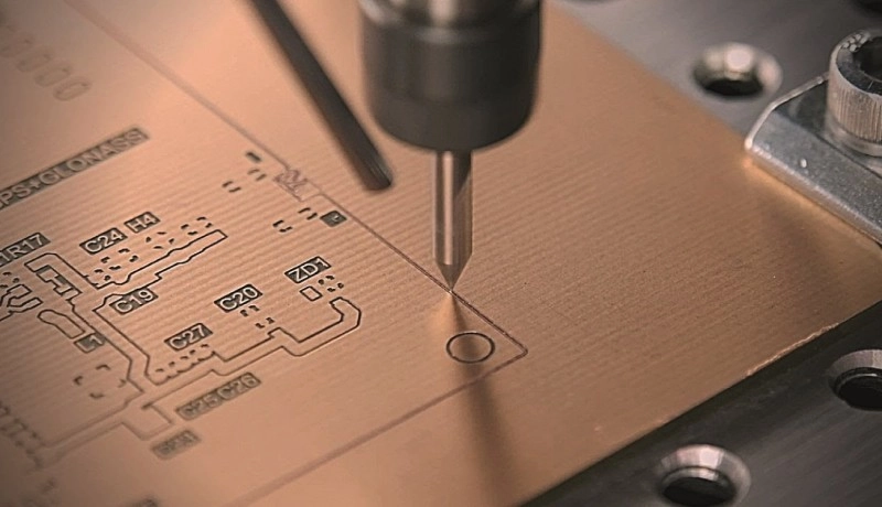
Milling
Milling is a mechanical PCB fabrication process that removes unwanted copper using a CNC (Computer Numerical Control) milling machine instead of chemical etching. It involves cutting precise traces, pads, and drill holes with a rotating tool. Materials like FR4, CEM-1, and aluminum can be milled, and software like FlatCAM and AutoCAD helps generate tool paths for CNC machines.
Tools
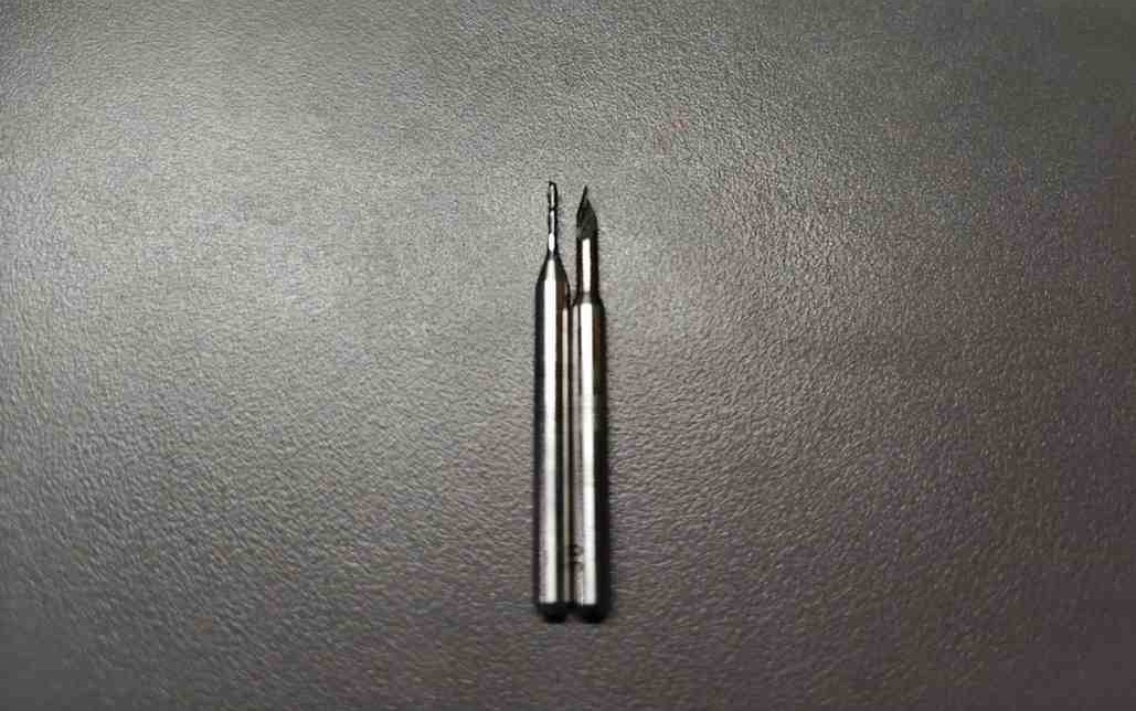
- End Mills (Flat or Square End) – Used for cutting traces and routing board outlines. Common sizes: 0.2 mm to 2.0 mm.
- V-Bit Engraving Tools – Used for isolating traces. They come in angles like 10°, 20°, 30°, or 60°.
- Drill Bits – For making holes for vias or component leads. Sizes typically range from 0.3 mm to 1.2 mm.
- Contour Routers – For cutting out the PCB shape from the material stock.
- Chamfer Bits – Used to create beveled edges or for edge cleaning.
Safety Precautions
- Wear Safety Gear – Always use safety goggles and a dust mask to protect from flying debris and fine fiberglass particles.
- Secure the PCB Material – Firmly fix the board to prevent movement during milling.
.
- Tool Inspection – Check milling bits for wear or damage before use.
- Machine Safety – Never touch the tool while it's spinning; keep hands away from the cutting area.
- Emergency Stop – Ensure the machine has an accessible emergency stop button.
For my Electronic Production assignment I am planning to do the milling method to make the PCB board.
In our lab we have the WEGSTR PCB milling machine,
Kicad
After designing the PCB you should export the PCB design either gerber file or SVG file format for further next operation.
In my case I export it SVG file format.
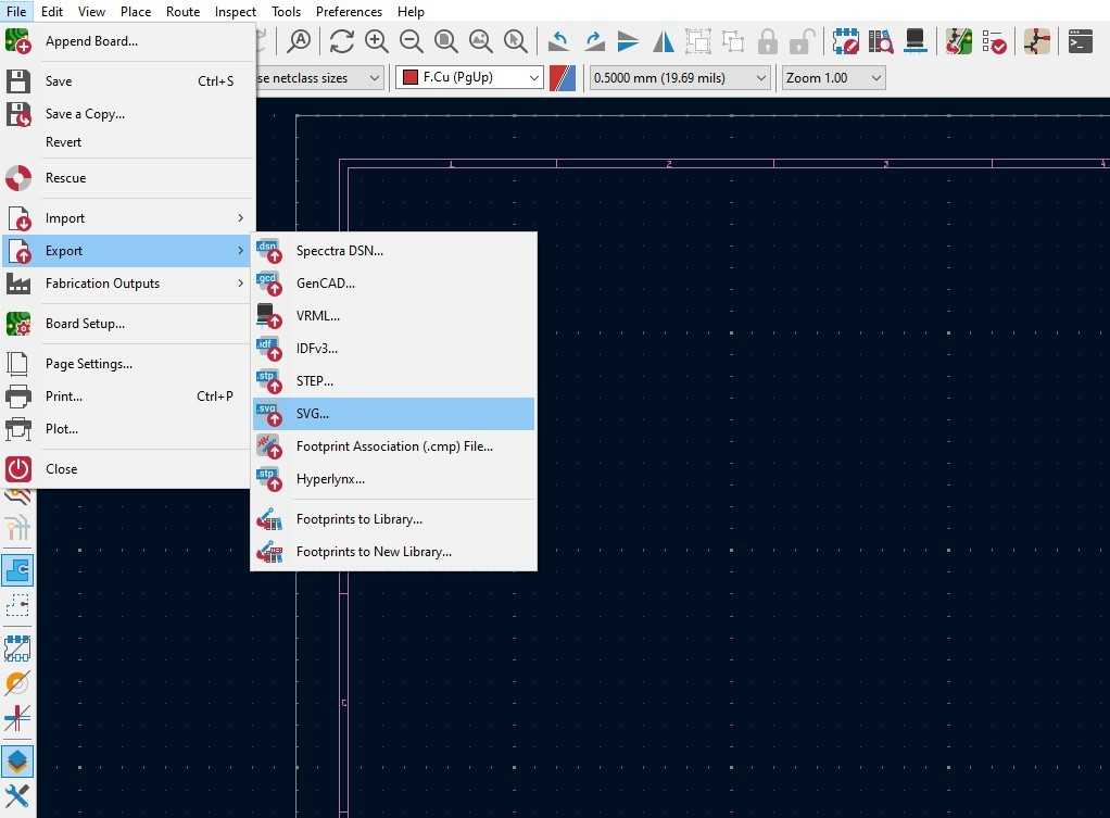
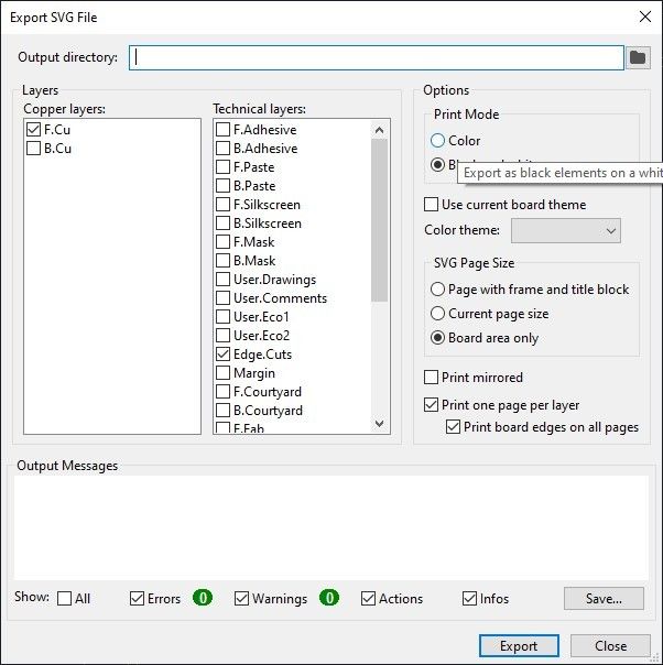
In Export option only select the F.Cu and Edge.Cuts, and also I selected the black and white colour of the file to see it clearly. In page size you should select the board area only otherwise the design take all ove the design like the tabulation you will see the right corner bottom. Then export it as per your destination.
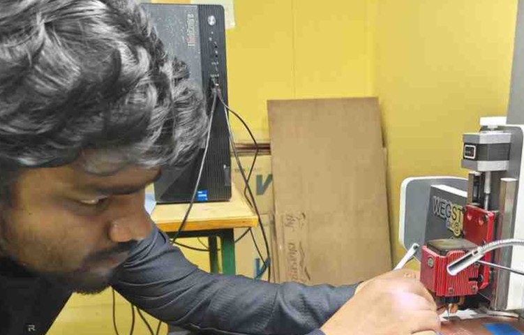
Tool and Board Setup
At first I placed one PCB board and then clamped the PCB board to the machine base with the help of tightening the corner holders. Clean the board with some soft cloth to remove the dirt above the layer.
Then I Set the V-bit tool 30 degree andgle to the machine for the milling operation, further cutting operation I will use the cutting tool
MODS
MODS CE (Community Edition) is a browser-based tool for digital fabrication workflows. It allows us to build modular workflows by connecting blocks for tasks like PCB milling and G-code generation. We can use it for machines like Roland SRM-20, 3018 CNC, and more.
.
Right-click to open a program and go to the G-code 2D PCB Milling, after enter into that load files PNG/SVG for processing (Right click>Program>open program>G-code - mill 2D PCB)
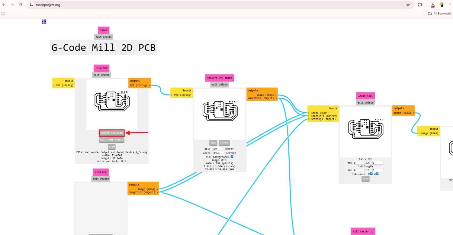
After load the SVG image you should set the proper parameters for our milling and cutting operation.
In below you can select the tool size for the millling process
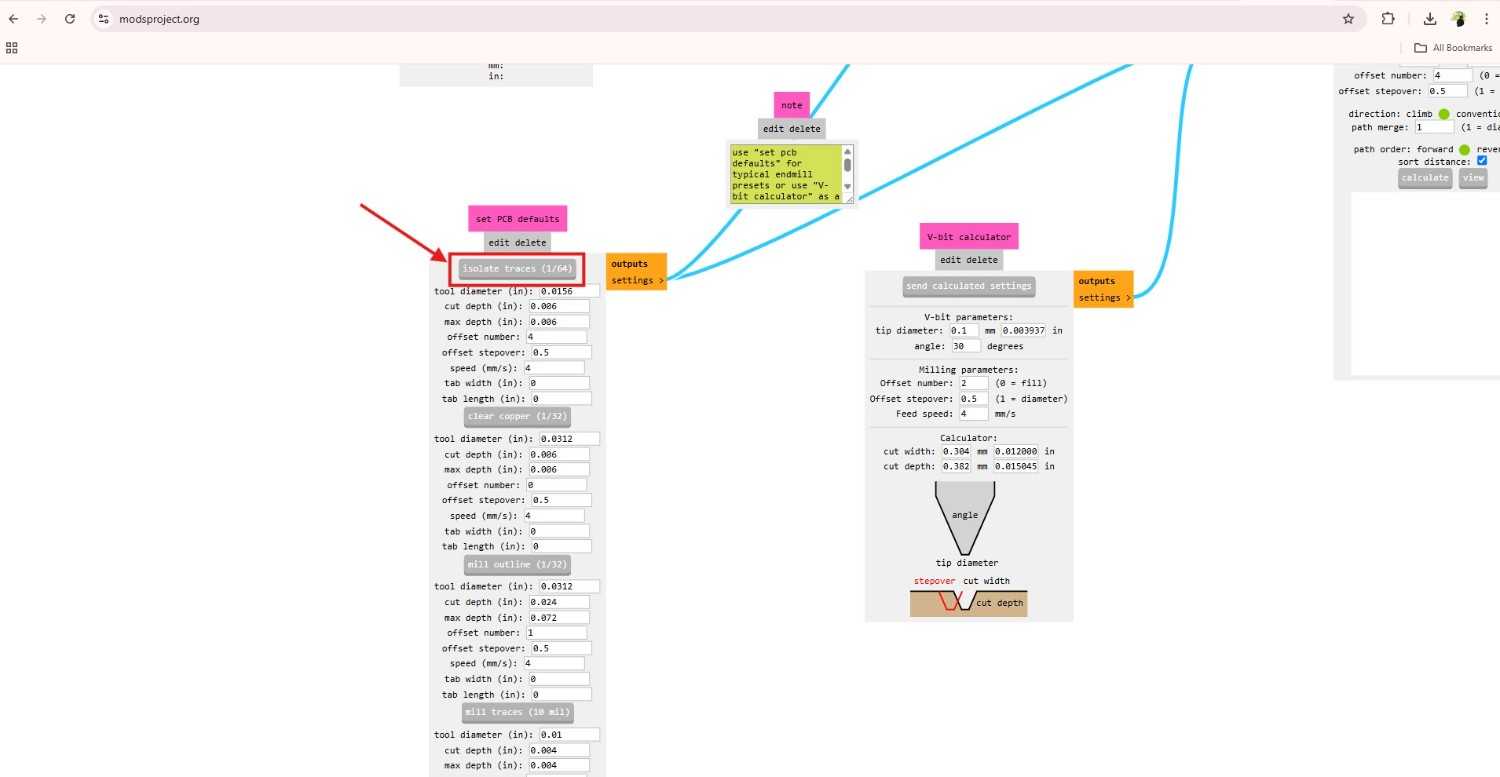
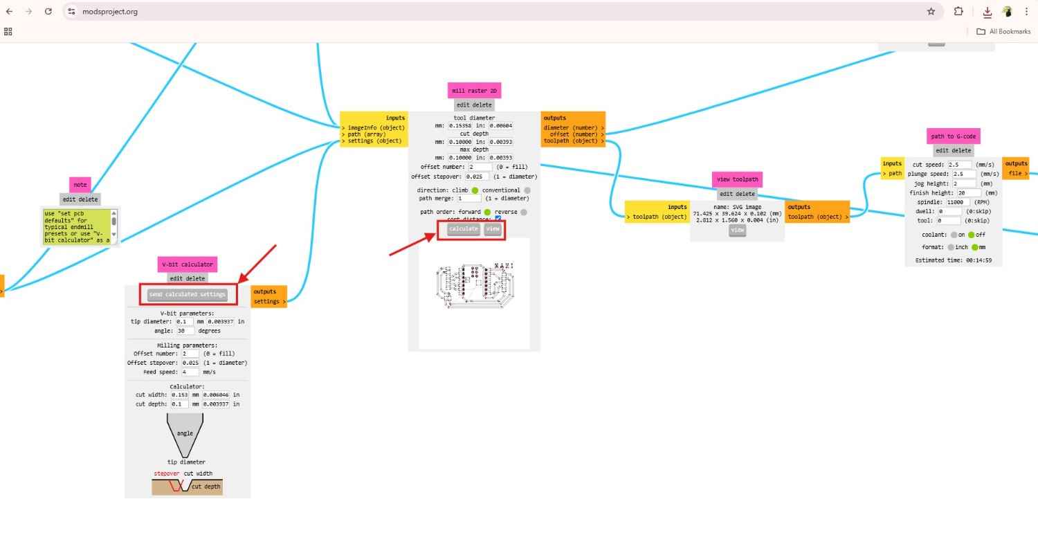
In my case I select the V-bit 30 degree, then in V-bit calculator you should calculate the required parameters according to your design.
After check the trial and error of all paramters I found out my design will be came good this settings.
I give the offest number 2, offset stepover 0.025 and cut depth 0.1mm.
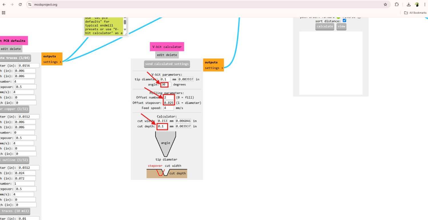
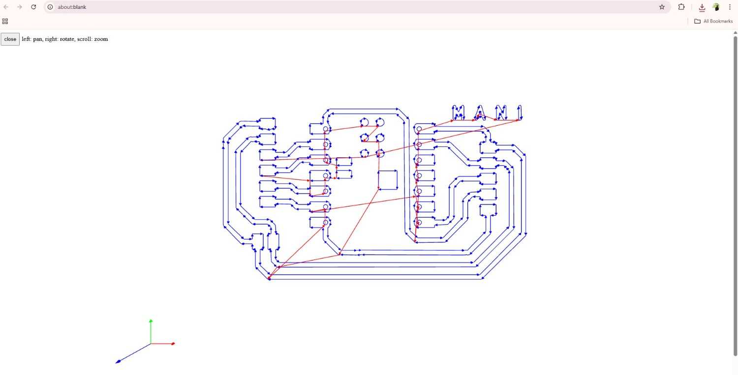
After done all that give the calculate in V-bit calculator, it will show up the mill raster 2D then again click the calculate in mill raster 2D without change any paramteres. The G-code will calcualte and dowload it automatically, you also check the tool path of the pcb design.
Wegstr
WEGSTR is a browser-based software used for generating G-code for CNC machines. It allows users to create toolpaths from vector drawings easily without needing advanced CAM software. The platform supports simple operations like engraving, drilling, and milling 2D shapes.
I used the Wegstr software to interact the PCB milling machine, I import the gcode which is I download from the Mods.
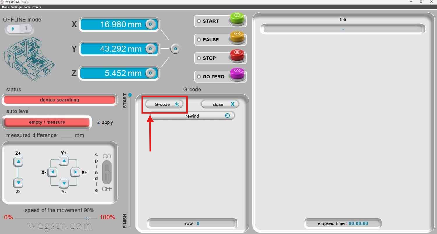
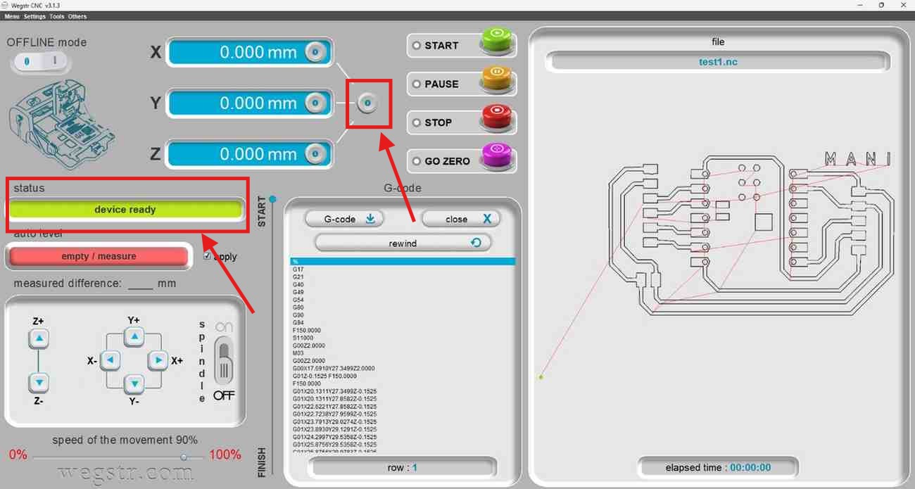
Turn on the milling machine, connect the machine with Wegstr software by using the USB port, you can see the machine is not ready, so you turn on the ready switch in Milling machine. We will ensure by seeing the switch is glowing without get constant lightning.
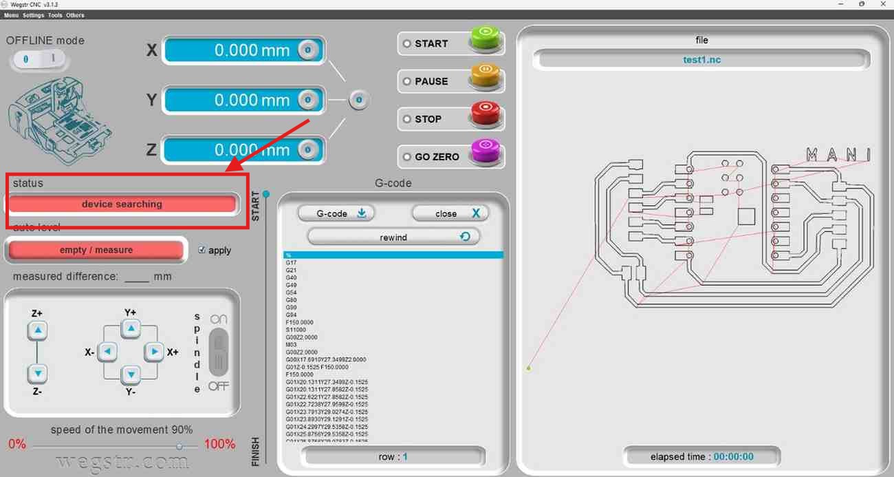
After that you can see the machine is ready, then I moved manually the spindle with the help of Wegstr software, set the correct place in x, y & z axis.
We have the auto leveling option in our machine but unfortunately in our machine’s autoleveling checker wire is missing so I manually set the machine depth by adjusting the z axis movement by touching the tool tip in the PCB board little bit at that time I didn’t fully tight the tool with the spindle because if you give extra depth little bit the tool will broken, after the tool tip touch the PCB I tightening the tool and set the origin.
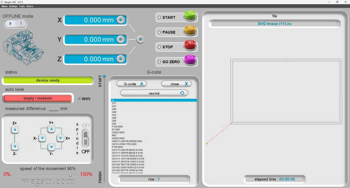
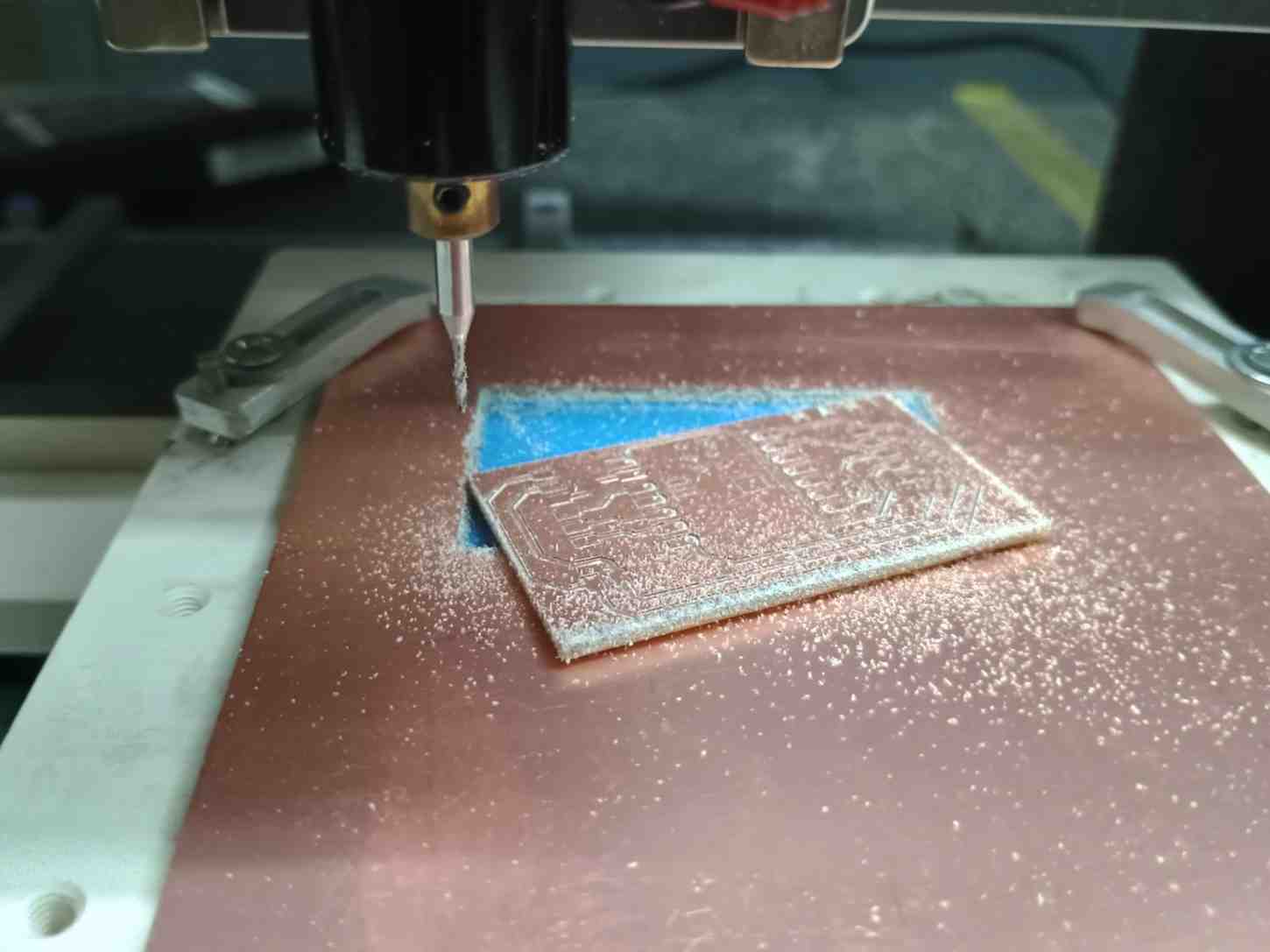
Milling Progress
Then start the milling operation, the spindle is start to rotate and move to the milling position.
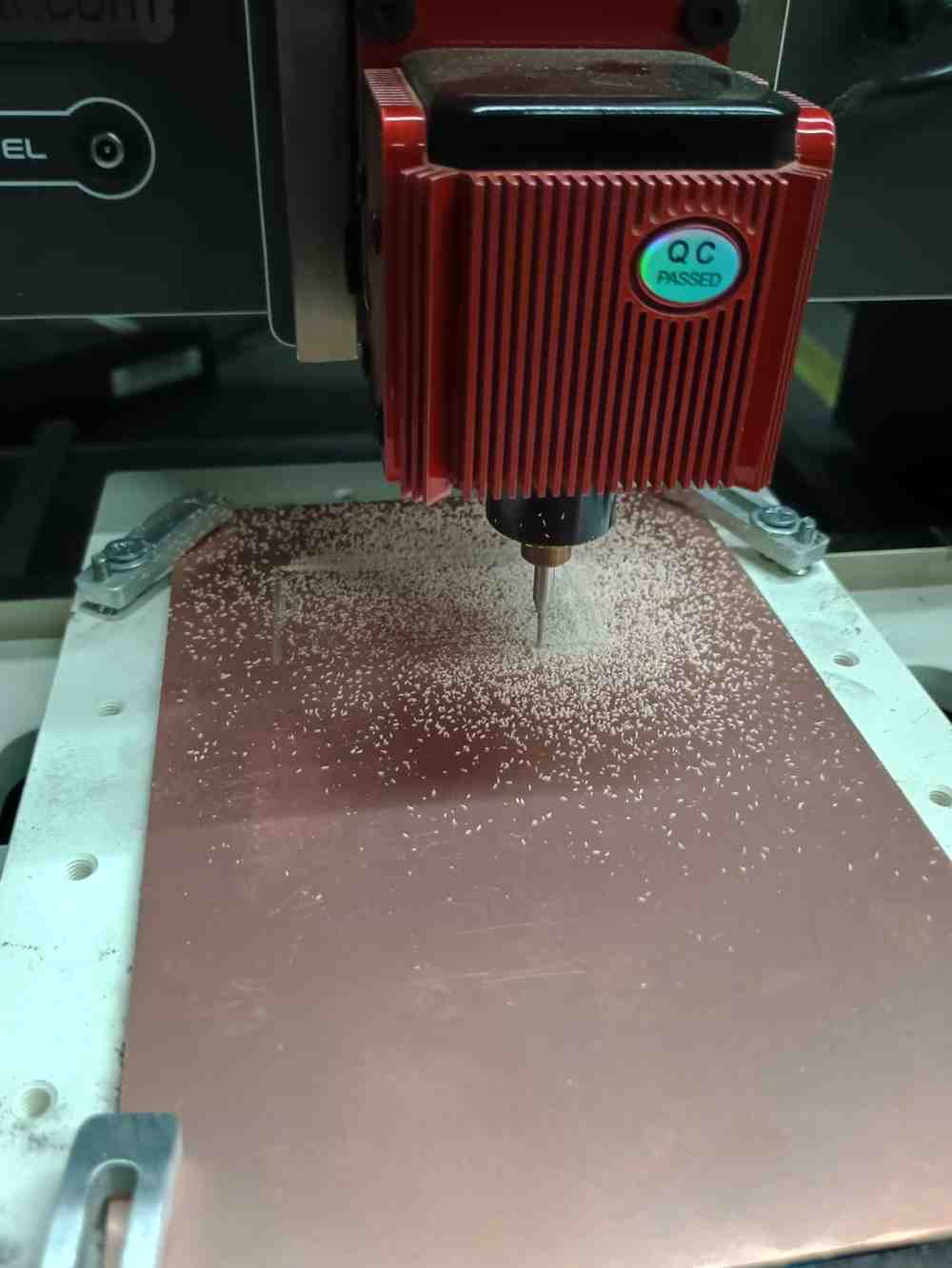
After did the milling, without changing the position we need to do the cutting process of our board, with adjusting the cutting tool bit into the spindle.
Again in ModsCE I change the tool, cut depth and offset, calculate my cutting outer rectangle board.
Then load it into the Wegstr software, gave the start to cutting process, the spindle is passing to the board, I set the 4 pass for cutting but it has completely cut out within 3 pass so I stop the machine and took out the cutting board.
Soldering
I checked the board whether the trace cuts came good or not with the help of multimeter by following the traces at pointing it in different locations.
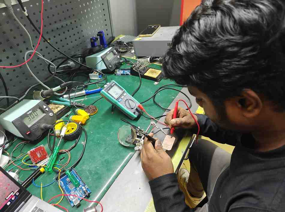
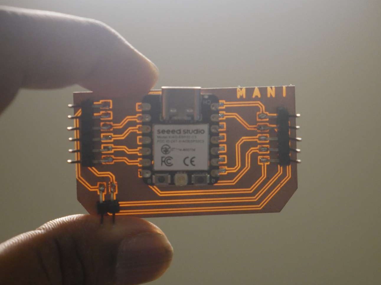
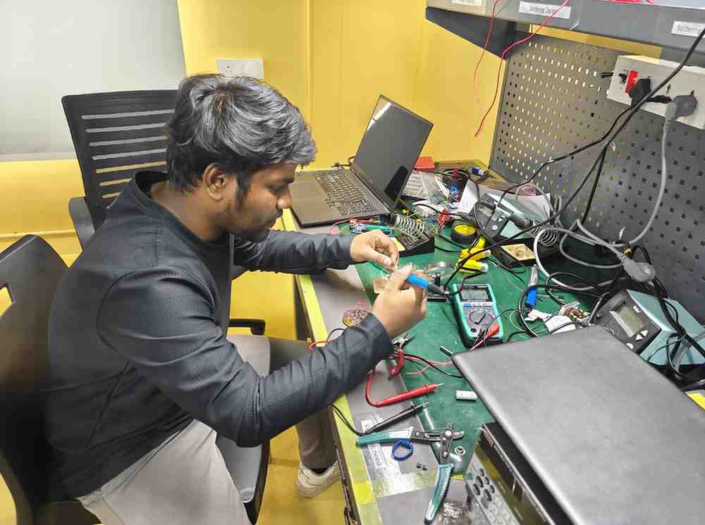
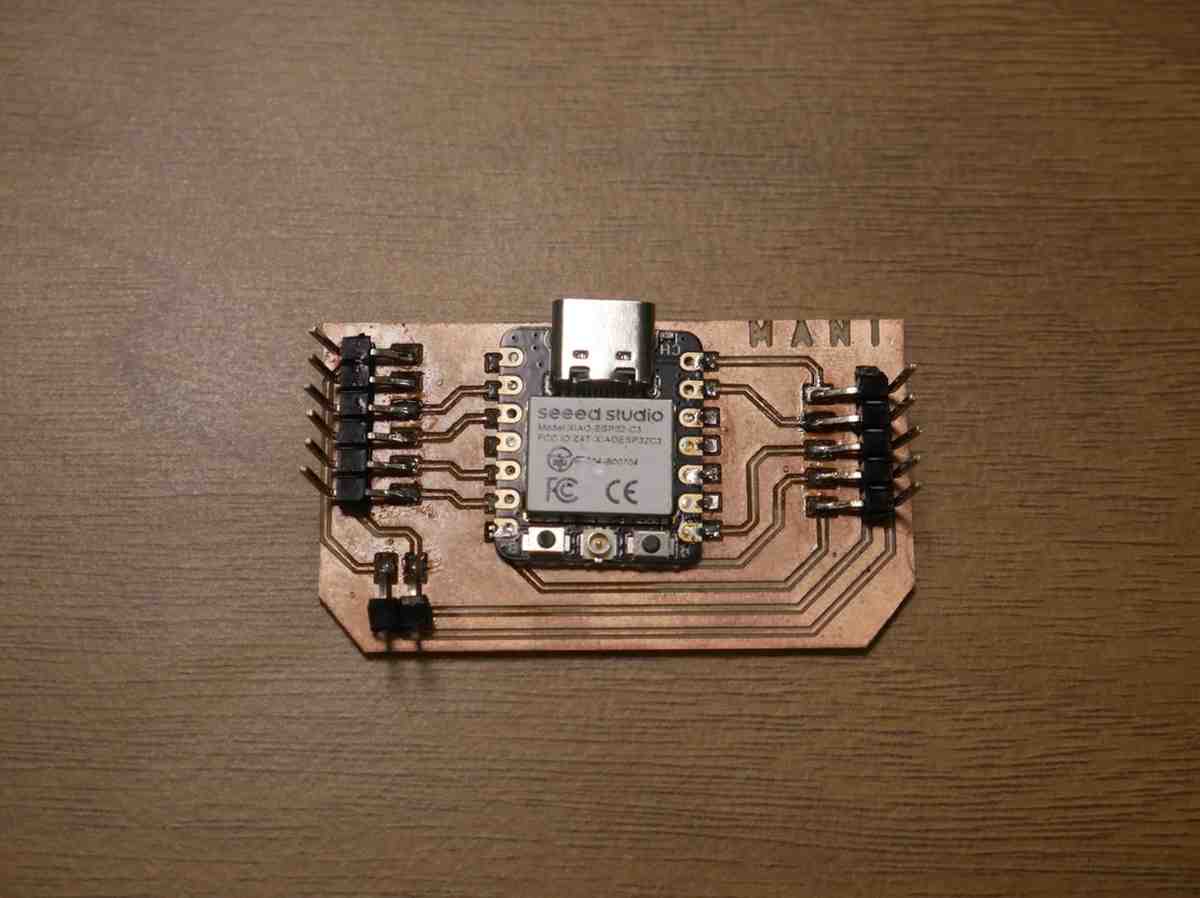
Then I did the soldering board with the seeed studio XIAO ESP32 C3
I haven’t soldering before that much, so at first I practice with some normal boards because the SMD components soldering is too critical for the beginners.
After done so much practice I got some courage to solder my PCB board
I start the soldering with the microcontroller
Testing
Here I updated my Output device week assingment working video of this fabricated board
The board is broken mistakenly, so I update the week 9 assignment here to show my board is functionally working after the whole process.
If you want to know more about week 9 assigment you can go and refer my Output Device assigment.
Here you can you this code to perform this work
#include <ESP32Servo.h>

#define ESC1_PIN D4  // Left motor
#define ESC2_PIN D5  // Right motor

#define JOY_X_PIN A1
#define JOY_Y_PIN A2

Servo esc1;
Servo esc2;

void setup() {
  Serial.begin(115200);

  pinMode(A1,INPUT);
  pinMode(A2,INPUT);
  pinMode(ESC1_PIN,OUTPUT);
  pinMode(ESC2_PIN,OUTPUT);
  esc1.attach(ESC1_PIN);
  esc2.attach(ESC2_PIN);

  esc1.writeMicroseconds(1000);
  esc2.writeMicroseconds(1000);
  delay(2000);  // Let ESCs initialize


}

void loop() {
  int xValue = analogRead(JOY_X_PIN);
  int yValue = analogRead(JOY_Y_PIN);
delay(1000);
Serial.println("start");
  Serial.print("X: ");
  Serial.println(xValue);
  Serial.print(" | Y: ");
  Serial.println(yValue);


  int pwmLeft = 1000;
  int pwmRight =1000;

  // Forward motion (both motors)
  if (yValue >3800) {
    int pwm = map(yValue, 3800,4095, 1000, 2000);
    pwmLeft = pwm;
    //analogWrite(ESC1_PIN,pwm);
   // analogWrite(ESC2_PIN,pwm);

    pwmRight = pwm;
    Serial.println("Moving Forward");


  // Backward motion (optional)
  /*else if (yValue < 400) {
    int pwm = map(yValue, 0, 400, 0, 1000);
    pwmLeft = pwm;
    pwmRight = pwm;
    Serial.println("Moving Backward");
  }
   */
  // Turning left or right by adjusting individual motor speeds
  }else if (xValue < 3000) {
    int turnPWM = map(xValue,  3000, 0,1000, 2000);
    pwmRight = turnPWM;  // Slow down right motor
    Serial.println("Turning Left");
  } else if (xValue > 3800) {
    int turnPWM = map(xValue, 3800, 4095, 1000, 2000);
    pwmLeft = turnPWM;  // Slow down left motor
    Serial.println("Turning Right");
  } else
  {
     esc1.writeMicroseconds(1000);
     esc2.writeMicroseconds(1000);
     Serial.println("Moving ");
  //delay(2000);
  }


 esc1.writeMicroseconds(pwmLeft);
  esc2.writeMicroseconds(pwmRight);

  delay(1000);
}
Conclusion
Learning outcomes
- Understood the complete PCB milling workflow, from clamping the board to final soldering and testing.
- Gained hands-on experience using MODS CE for generating G-code from SVG files, and correctly setting milling parameters like cut depth, offset, and stepover.
- Learned to use a V-bit 30° tool and calculated its parameters using a V-bit calculator to ensure precision milling.
- Successfully carried out both the milling and cutting operations, understanding tool changes and pass settings for complete board separation.
- Used a multimeter to verify trace connectivity and ensured the milled PCB was functional before soldering.