Week 06 - Electronics Design

Group assignment:
• Use the test equipment in your lab to observe the operation of a microcontroller circuit board (as a minimum, you should demonstrate the use of a multimeter and oscilloscope)
• Document your work on the group work page and reflect what you learned on your individual page
Individual assignment:
• Use an EDA tool to design a development board that uses parts from the inventory to interact and communicate with an embedded microcontroller
Group assignment
For this week’s Group assignment, I teamed up with my fellow Fab Academy buddy Haw Ren to use the test equipment in our lab to observe the operation of a microcontroller circuit board.
The documentation for our Group assignment can be found here.
Group assignment reflection
From the eyes of absolute beginners, I found that these testing tools look very complicated and intimidating with lots of readings, buttons, symbols and settings, they eventually make more sense when we tried using them and learnt more about their purpose and functions. I found that certain features where useful in reducing the complexity of using some of these devices. My favourites were:
• Auto-ranging on the multimeter that allows measurements without having to worry about setting the correct range.
• The output button on the bench power supply that allows you to only power a circuit on when you are ready to test it.
• Automatic frequency measurements on the oscilloscope
Individual assignment
Overview
For the individual assignment, I will use Autodesk Eagle to design a board for the Seeed Xiao RP2040, so that it can connect to external components easily. I will also add a push button and an LED so that additional functions can be performed with just this board itself.
PART A: Schematic
Copy Libraries to Eagle
I start by downloading and copying some libraries to Eagle. I downloaded the following libraries:
• Sparkfun
• Fab
• XIAO RP2040
The next step is to copy them to the Eagle libraries folder. In my case, it was C:\Users\cflor\OneDrive\Documents\EAGLE\libraries. Libraries are a convenient way to add electronic components to the board design so that you do not need to create components from scratch.

Create a New Project
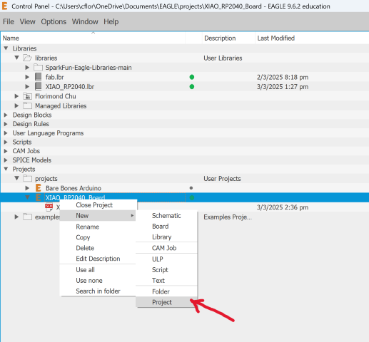
To start a new project, go to the projects folder, right-click and select “new project” to create a new project. Give the project a name. I named mine XIAO_RP2040_Board.
Create a New Schematic
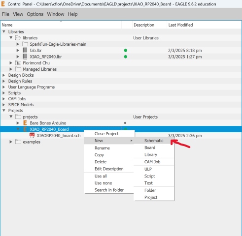
Similar to the new project process, right-click and select “new schematic” to create a new schematic under the project name.
Adding Parts to the Schematic
The next step is to select the components to put into the schematic. Using the “Add” shortcut of CTRL+SHIFT+A, bring up the “Add” dialogue box. Search for the components you need from the libraries that were downloaded previously.
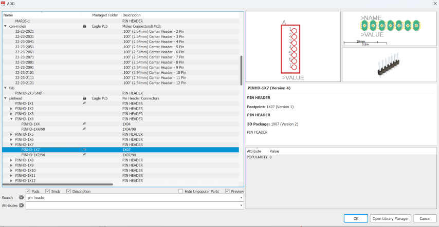
Once you find the components, lay them onto the schematic.
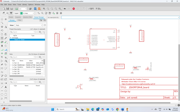
Here is a list of components that I laid down:
| Part | Value | Device | Description | Package | Library |
|---|---|---|---|---|---|
| JP1 | PINHD-1X7 | Pin Header | 1X07 | pinhead | |
| JP2 | PINHD-1X6 | Pin Header | 1X06 | pinhead | |
| JP3 | PINHD-1X5 | Pin Header | 1X05 | pinhead | |
| JP4 | PINHD-1X5 | Pin Header | 1X05 | pinhead | |
| R1-10KOHMS | 10kOHMS | RES-US1206FAB | Resistor for Push Button | R1206FAB | fab |
| R2-1KOHM | 1kOHMS | RES-US1206FAB | Resistor for LED | R1206FAB | fab |
| S1 | 6MM_SWITCH6MM_SWITCH | Push Button Switch | 6MM_SWITCH | fab | |
| U$1 | LEDFAB1206 | LEDFAB1206 | LED | LED1206FAB | fab |
| U1 | 102010428' | 102010428' | XIAO RP2040 module | MODULE_102010428 | XIAO_RP2040 |
Wiring up the Schematic Using the Net function, I connect up the components to the XIAO RP2040 board in the schematic.
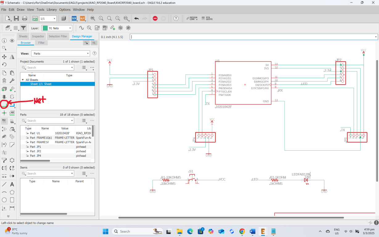
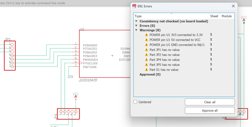
Running the ERC test With all the components connected up, I run the ERC (Electrical Rule Check). It gives me 8 warnings but none of them are critical. As such, I can proceed to the next section.
PART B: Board Layout
With the Generate/Switch to Board command, the schematic is automatically sent to the board editor, ready to be placed and routed.
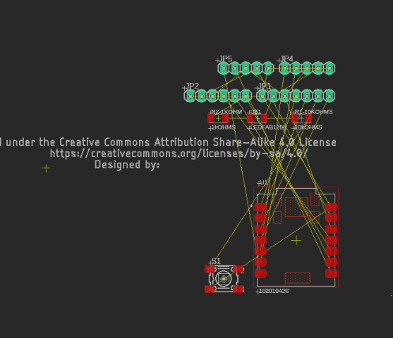
Settings
Before we route the components to the board, there are some settings to take care of…
Grid Settings
Set the Grid as follows:
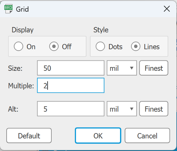
DRC (Design Rules Check) Settings
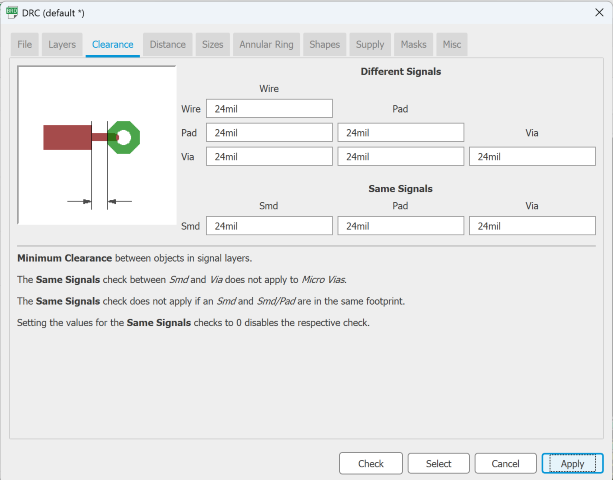
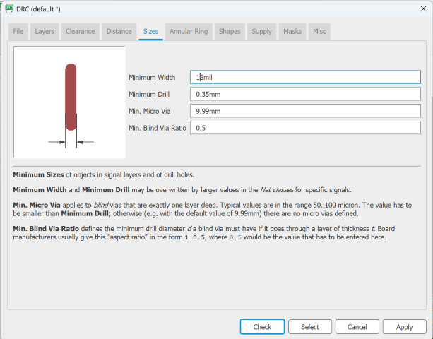
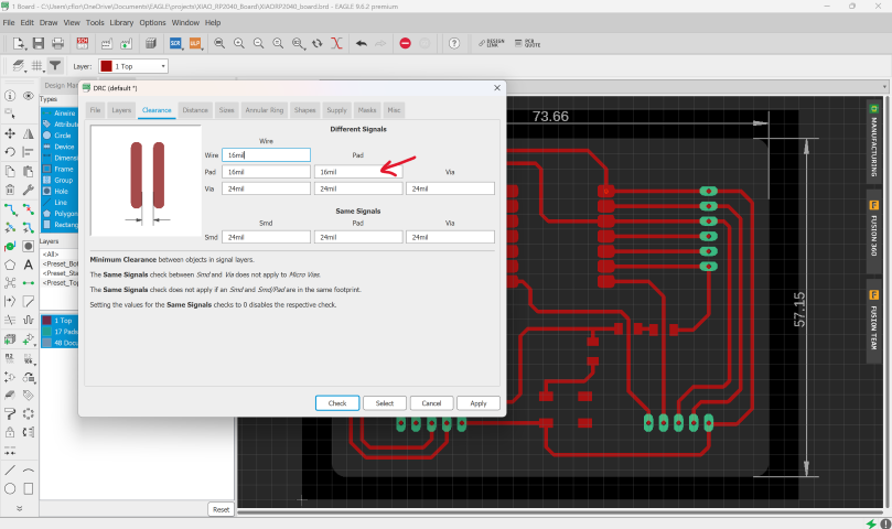
These settings in the DRC help to ensure that there is enough space and clearance between the paths so that the board can be milled.
Set the Clearance:
Set the Size:
Routing the Airwires
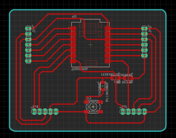
Once the settings have been input, I start to route the airwires. The goal is to create paths for your circuit board so that they can be milled on a CnC machine. Here are some things that I observed when doing the routing:
1. Try to avoid 90-degree angles
2. Do not overlap the wire routes
3. No vias. I learnt that we will be doing a single layer board, so I avoided doing vias.
4. Do not have the paths routed too close together. They may accidentally cause short circuits when you solder components on the board.
After some tinkering with the routing, I draw an outline for the board and I am done!
Post-routing Checks
After routing, I ran the following checks:
Ratsnest check
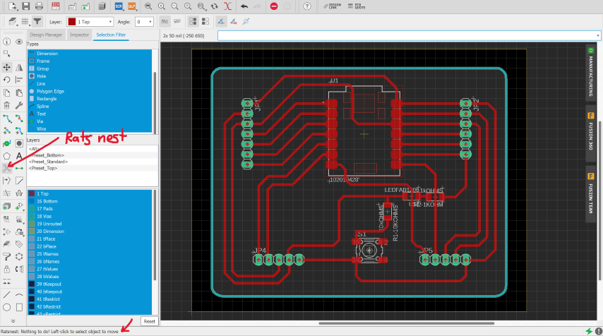
A ratsnest check visually displays all unrouted connections on a PCB layout as lines, showing where wires need to be drawn to complete the circuit. It helps identify areas needing routing by highlighting unconnected pads and pins. Simply click on the ratsnest button and if okay, it says “Ratsnest: Nothing to do!”
DRC check
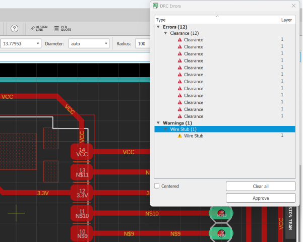
I ran into some warnings while performing the DRC checks. Most of them are clearance issues due to pads being too big on the RP2040 module that I downloaded. I can fix those in photoshop so I will not be fixing them here.
UPDATE/CORRECTION (18 June 2025)
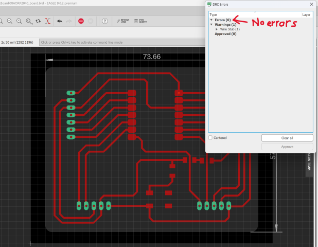
Fixing the DRC clearance errors in photoshop is an unconventional method. The DRC clearance errors should be rectified using the DRC tool check (Tools > DRC). While I initially received an error because the DRC clearance was set too large at 24 mil. However, I confirmed with my instructor that a 16 mil clearance would be sufficient for my board. I changed the clearance value to 16 mil and ran the DRC check again. This time there were no clearance errors.
Exporting the PNGs
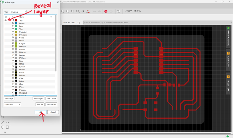
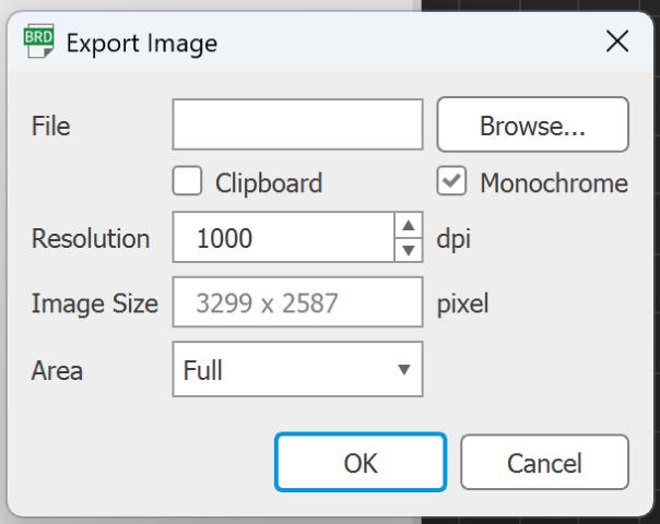
You will need the PNG images to create the g-code files for the CNC milling process later on. To export PNGs, first go to the Layer Settings to turn on the visibility of the objects you want to export.
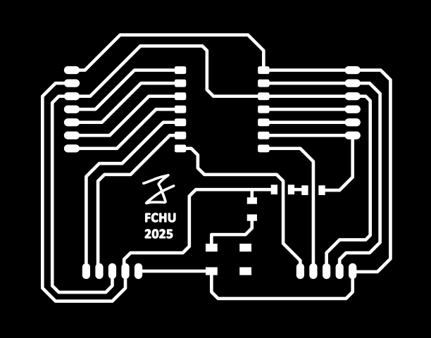
Next, choose the correct export settings (monochrome and 1000 dpi), and then export the images. I exported the outline, pads and circuit path as 3 separate files so that I can work on them separately.
I did a bit of post-editing in photoshop to add some graphical elements and do some simple touch-up. Below are my final PNGs (one file for the circuit, the other for the outline).

Once I have the PNGs, I follow the steps below from former Fab Academy Student Juliana to generate the G-code file from the mods page:
1. Open the MODS PAGE
2. Right click on the screen and choose Programs from the menu
3. Then choose Server Program from the list
4. Scroll down to G-code, chose mill 2D PCB png
5. Once Mods windows are open, select open PNG file
6. At the third window we select Calculate
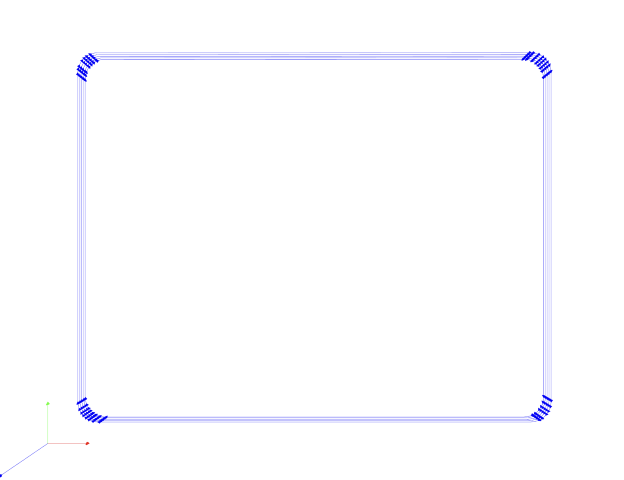
7. Select view to see the G-code path
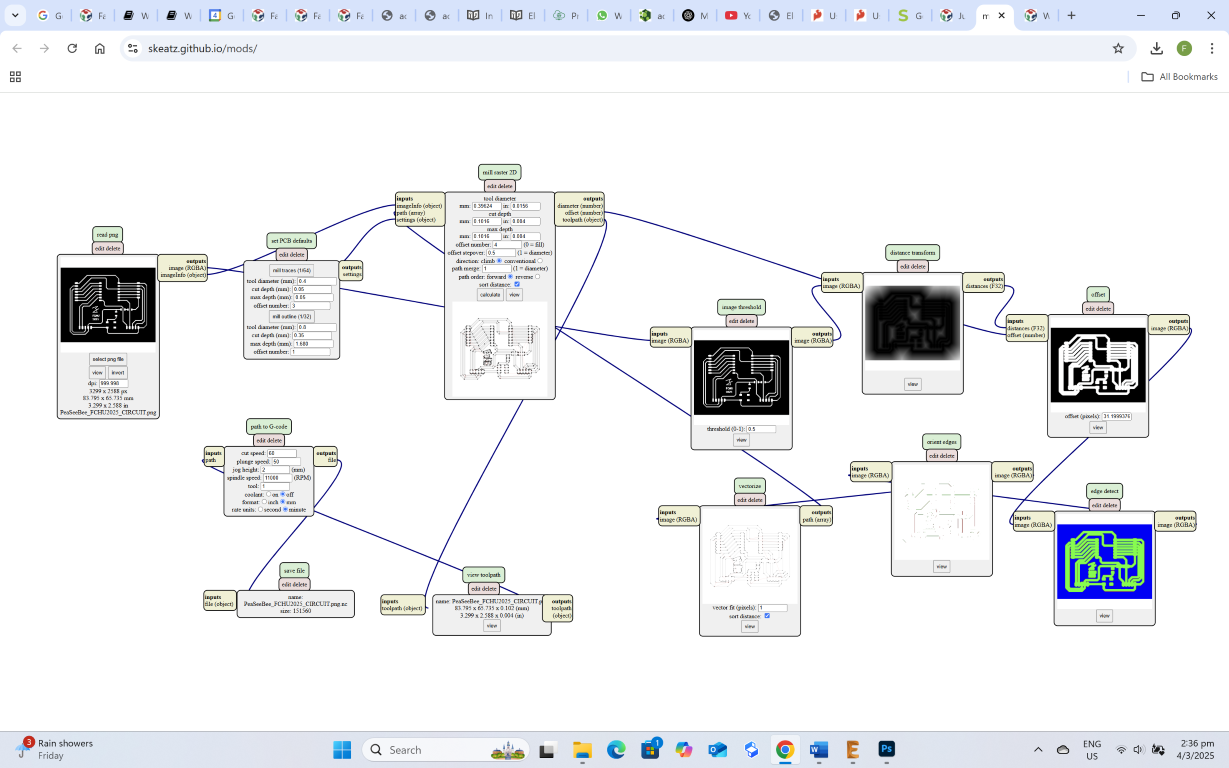
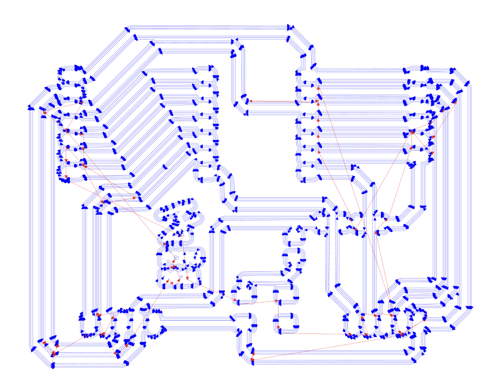
To get the NC files for the outline, I repeat the process above. The only thing I changed was instead of selecting the "mill traces (1/64)" option, I choose "mill outline (1/32)" before generating the outline NC files.
This concludes this week’s assignment. Being new to electronics design, this week was a tough one for me, but I pulled through. I still have a lot to learn but this is what Fab Academy is about. Onward!
Files:
Eagle Board File (Right click > Save link as)
Eagle Schematic File (Right click > Save link as)
Resource Links:
Throughout this week’s assignment, I referred to these tutorials to help me through the board design process:
https://learn.sparkfun.com/tutorials/using-eagle-schematic
https://learn.sparkfun.com/tutorials/using-eagle-board-layout#previously-on-using-eagle
