Assignment Brief:
- Use a multimeter to measure voltage levels and an oscilloscope to analyze signal waveforms on the microcontroller circuit.
- Reflect individually on what was learned about signal behavior, power characteristics, and troubleshooting.
- Use an EDA tool to design a development board with inventory parts, ensuring proper power distribution, I/O headers, and communication interfaces.
Electronics Design
This documentation covers essential topics related to microcontroller circuits, electronic components, PCB design, simulation, and testing. By studying these concepts, I learn't how to work with electronic components, design and fabricate PCBs using EDA tools, simulate circuits for analysis, and tested microcontroller-based systems with various lab equipment. These skills are crucial for developing and troubleshooting embedded systems.
Firstly, I familiarized myself with the key terms and references introduced during the lecture on Wednesday. This included understanding various electronic components, circuit design principles, and the use of essential tools like multimeters and oscilloscopes. Below is the documentation of my learning
Microcontroller Circuit
Connectors & WiresConnectors and wires are essential components in electronics that help establish electrical connections between different parts of a circuit. Wires are conductive materials (usually copper) that carry electrical signals or power between components. Connectors allow easy attachment and detachment of wires and components without permanent soldering.
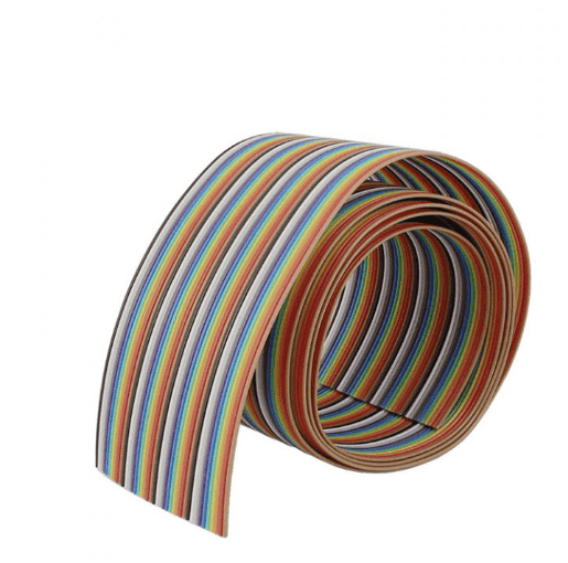
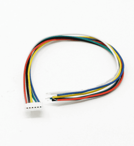
Ribbon cables are flat, flexible wires used for easy multi-wire connections, often with IDC (Insulation Displacement Connectors) for secure attachment. IDC connectors provide a reliable and quick way to connect ribbon cables to circuit boards without soldering. These are commonly used in microcontroller projects for interfacing multiple components. JST connectors are commonly used in electronics for secure, polarized connections between components, such as battery packs, sensors, and circuit boards.
Passive Components
Passive components are electronic components that do not require an external power source to operate. They simply respond to the electrical signals in a circuit and cannot amplify or control them like active components (e.g., transistors).
- Resistors: Limit current flow and divide voltage, following Ohm’s law (I = V/R).
- Capacitors: Store and release charge, available as unpolarized (ceramic) or polarized (electrolytic).
- Inductors: Store energy in a magnetic field and oppose sudden current changes (V =
L dI/dt).

Semiconductors
Semiconductors are materials that have electrical conductivity between that of a conductor (like copper) and an insulator (like rubber). Their ability to conduct electricity can be controlled, making them the foundation of modern electronics.
- Diodes: Allow current flow in one direction (PN, Schottky, Zener, LED).
- Transistors: Transistors are tiny electronic switches that control the flow of electricity in a
circuit.
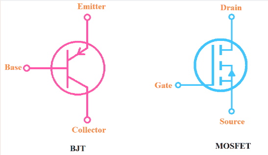
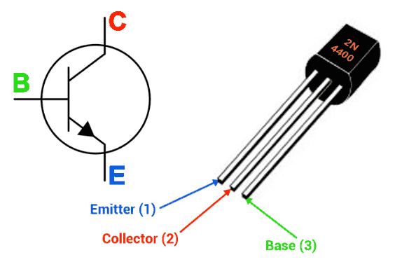 BJT (Bipolar Junction Transistor) has three pins: Collector, Emitter, and Base. The Base
controls.
the transistor, allowing current to flow from the Collector to the Emitter.
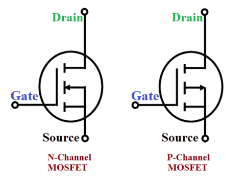
 - Mosfet: MOSFET (Metal-Oxide-Semiconductor Field-Effect Transistor) also has three pins: Source,
Drain, and Gate. The Gate works like a switch—when a voltage is applied to it, electricity flows
between the Source and Drain. Imagine it like an automatic door—when you press a button (apply
voltage to the Gate), the door opens (current flows from Source to Drain).
MOSFETS are of two types: N-Channel and P-channel, the key difference between the two is, Placement in Circuits N-channel: Preferred for low-side switching (between load and ground). P-channel: Used in high-side switching (between power and load). To know more about what_are_mosfets refer this Link. - Batteries supply direct current (DC) power, meaning the current flows in one constant direction. They are used in portable electronics, electric vehicles, and backup power systems.
- Voltage Regulators (Stable Power Supply): Regulators ensure a steady and consistent voltage output, preventing fluctuations that could damage electronic components.
- Temperature Sensors (DHT11, LM35, DS18B20) - Measure temperature.
- Light Sensors (LDR, TSL2561, BH1750) - Detect ambient light levels.
- Motion Sensors (PIR, Accelerometer, Gyroscope) - Detect movement and orientation.
- Proximity Sensors (Ultrasonic HC-SR04, IR Sensor) - Detect objects nearby without contact.
- Sound Sensors (Microphone, Sound Level Sensor) - Capture audio or detect noise levels.
- Touch Sensors (Capacitive Touch, Force Sensitive Resistor) - Detect touch or pressure.
- Motors (Servo, Stepper, DC Motors) - Enable movement in robotics and machines.
- Speakers & Buzzers - Generate sounds for alarms, notifications, and audio feedback.
- LEDs & Display Screens (OLED, LCD, 7-segment) - Provide visual feedback.
- Solenoids - Create linear motion, used in door locks and industrial applications.
- Relays - Act as electronically controlled switches for high-power applications.
- Vibration Motors - Provide haptic feedback in mobile phones and controllers.
- Push Buttons - Trigger actions when pressed.
- Toggle Switches - Maintain ON/OFF states.
- Rotary Encoders - Detect rotational movement and direction.
- Keypads - Provide multi-button input, useful for numeric and text entry.
- Power Supply: Provides stable voltage.
- Multimeter: Measures voltage, current, and resistance.
- Oscilloscope: Visualizes waveforms for signal analysis.
- Logic Analyzer: Captures digital signals for debugging communication protocols.
- Schematic Capture – Create and edit circuit diagrams with a vast library of components.
- PCB Layout Design – Convert schematics into PCB layouts and route traces.
- Simulation – Test circuits before manufacturing using built-in SPICE simulation.
- Component Library – Access thousands of components, including custom footprints.
- 3D PCB Viewer – Preview and inspect your PCB design in a realistic 3D model.
- Fabrication & Ordering – Export Gerber files.
- Go to EasyEDA.
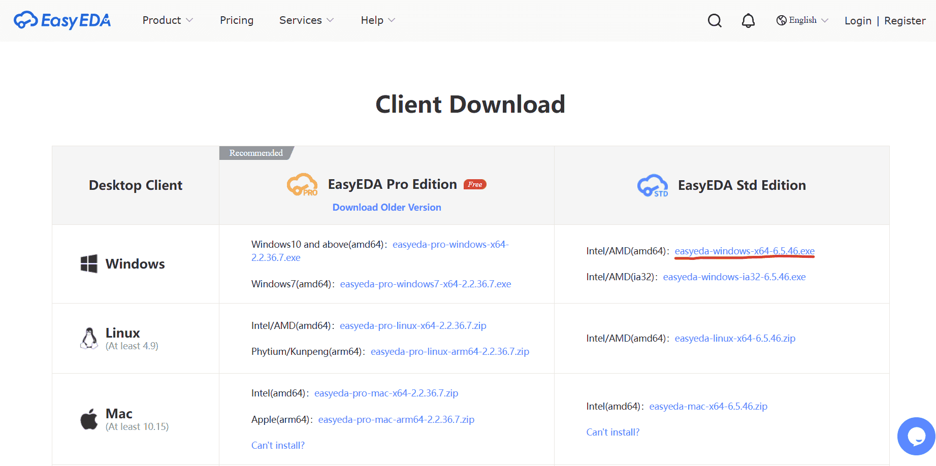
- Click "Sign Up" to create an account or "Log In" if you already have one.
- Once logged in, click "New Project" to start a new design.
- EasyEDA Interface
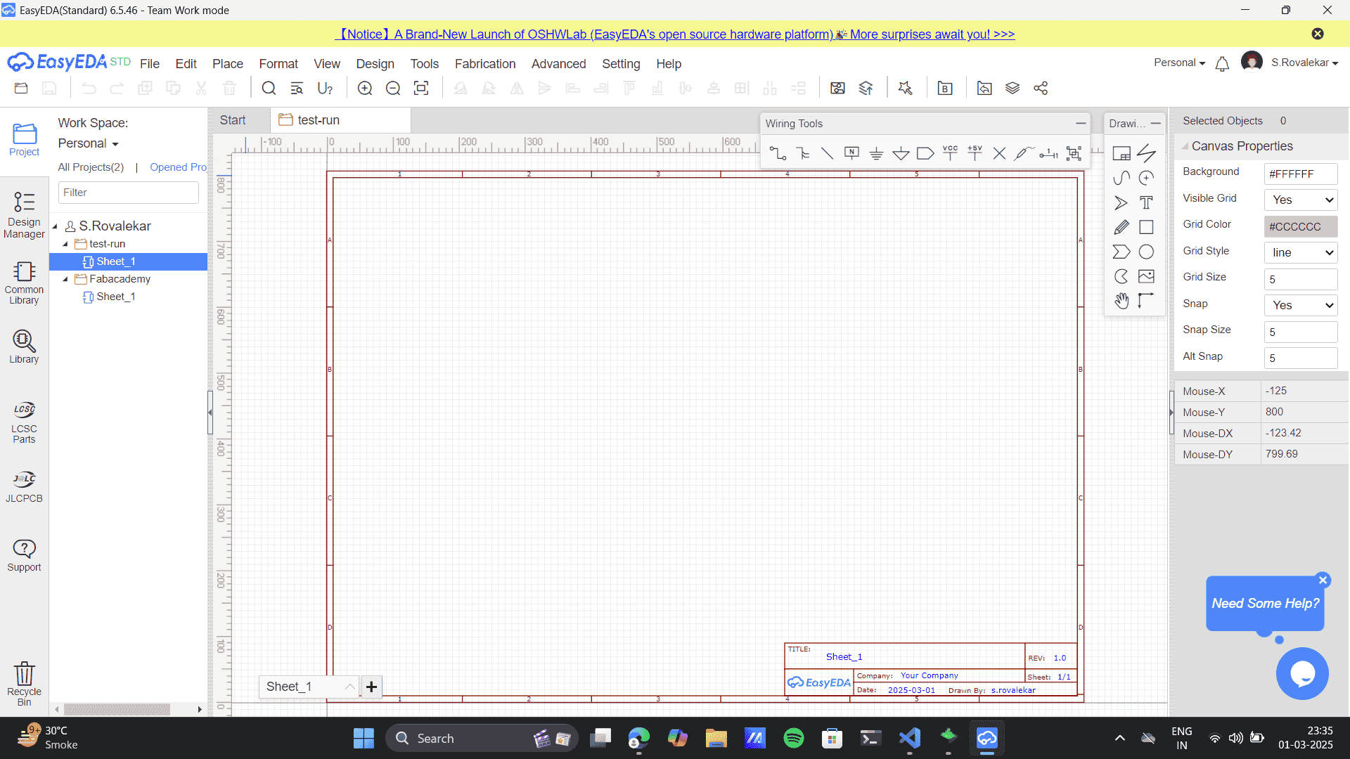
- Click on "Schematic Design" in the toolbar.
- Use the "Common Library" panel to search for basic components. Click on the component to add to the sheet.
- Use the "Library" panel to search for components (resistors, capacitors, ICs, etc.).
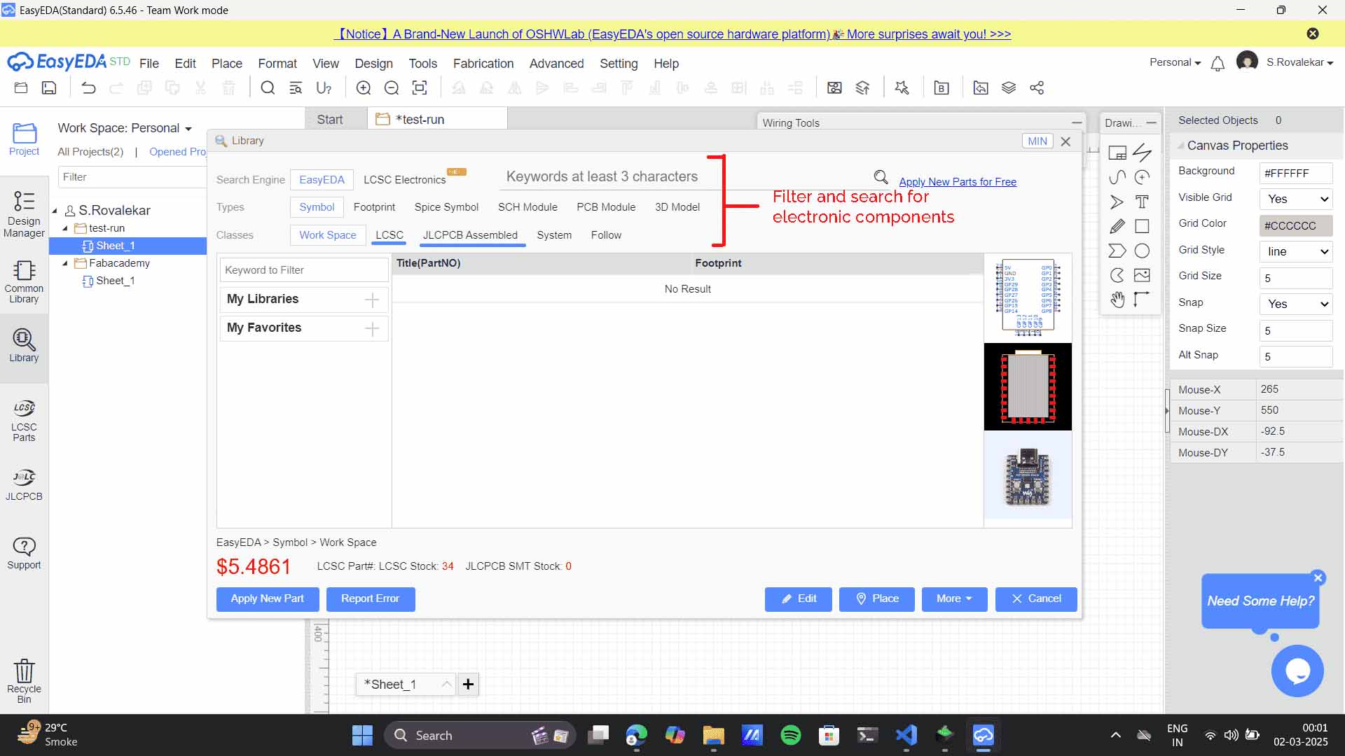
- Types of Components:
- Symbol: Used in schematic design (circuit diagrams).
- Footprint: The physical representation for PCB layout.
- Spice Symbol: Used for circuit simulation (SPICE-based analysis).
- SCH Module: Predefined circuit blocks.
- PCB Module: Predefined PCB layouts.
- 3D Model: View 3D representations of components for mechanical design.
- Classes of Components:
- Work Space: Components stored in the user's project.
- LCSC: Components sourced from LCSC, a popular electronic component supplier.
- JLCPCB Assembled: Components available for JLCPCB assembly services.
- System: Standard system components.
- Follow: Favorite or followed components.
My professor, Pranav Gawde suggested that searching for components is a a difficult task as the name specification and the precision of the component that we need might be different. He added, the LCSC and JLCPCB are the preferred filters for choosing the required component.
- Drag and drop components onto the schematic canvas.
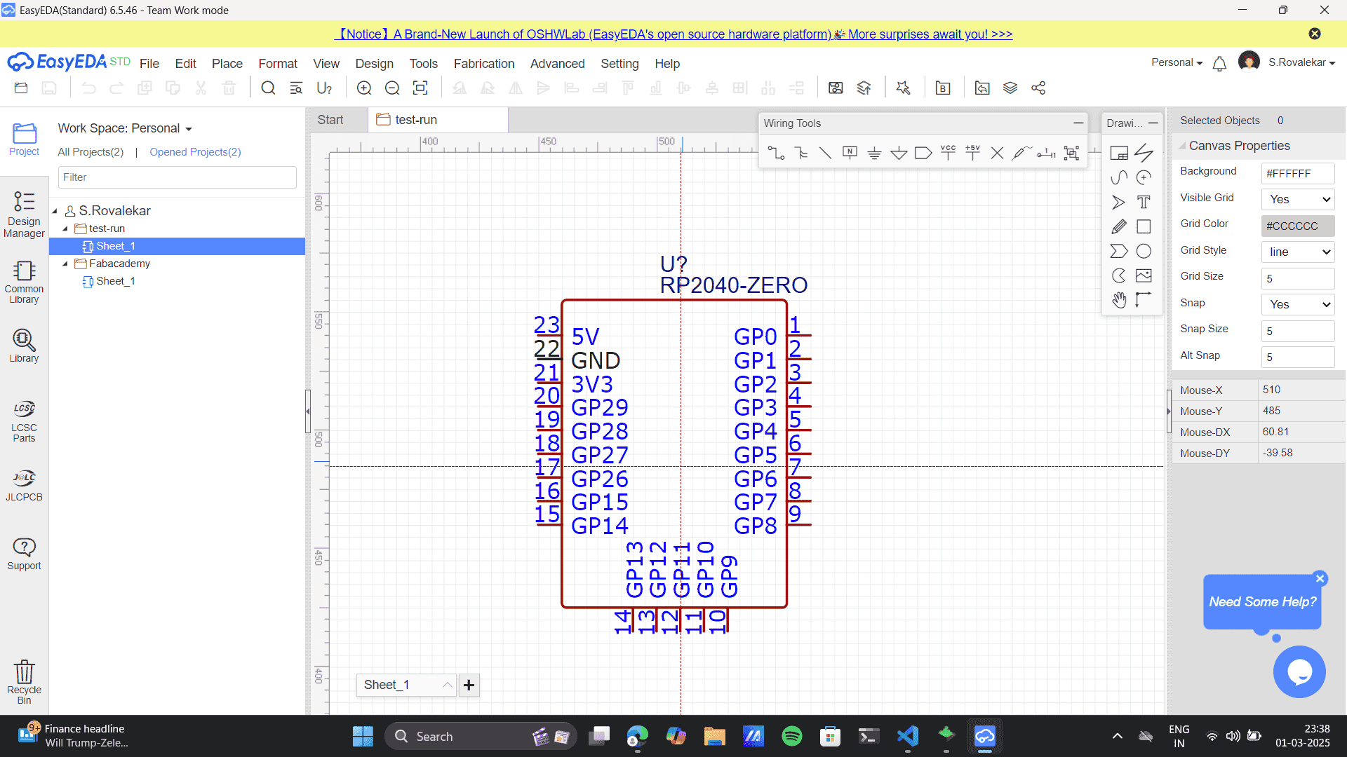
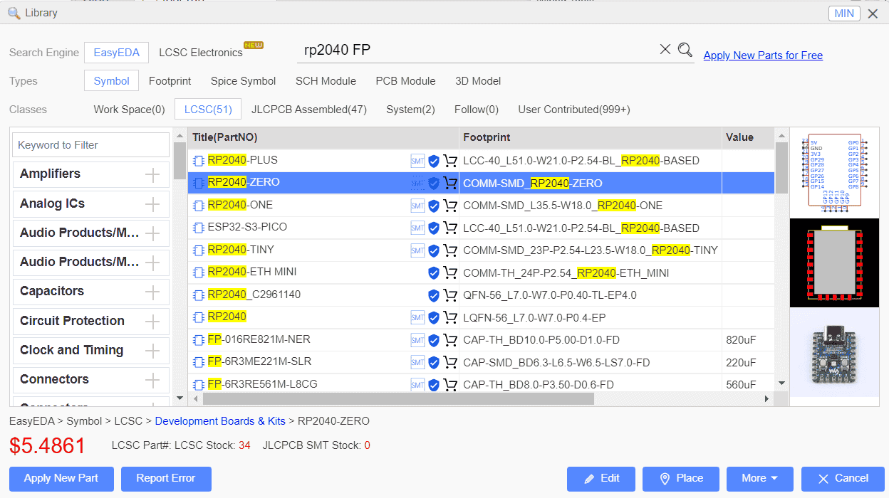 Here, I used an RP2040 from the library and placed it on the sheet.
- Place the componenent on the sheet. Later in the
process I realised the RP2040 that I choose here was not the
proper pin configuration that I required. However, I decided to design a basic circuit schematic for
which
I used the same XAIO RP2040.
- To understand the basics of EasyEDA, I planned to design a simple circuit using the RP2040
microcontroller, a push-button switch (SW1), and an LED (LED1) with a 1kΩ resistor (R1).
Thus, from the common library and library panel I placed all the required components to the
sheet.
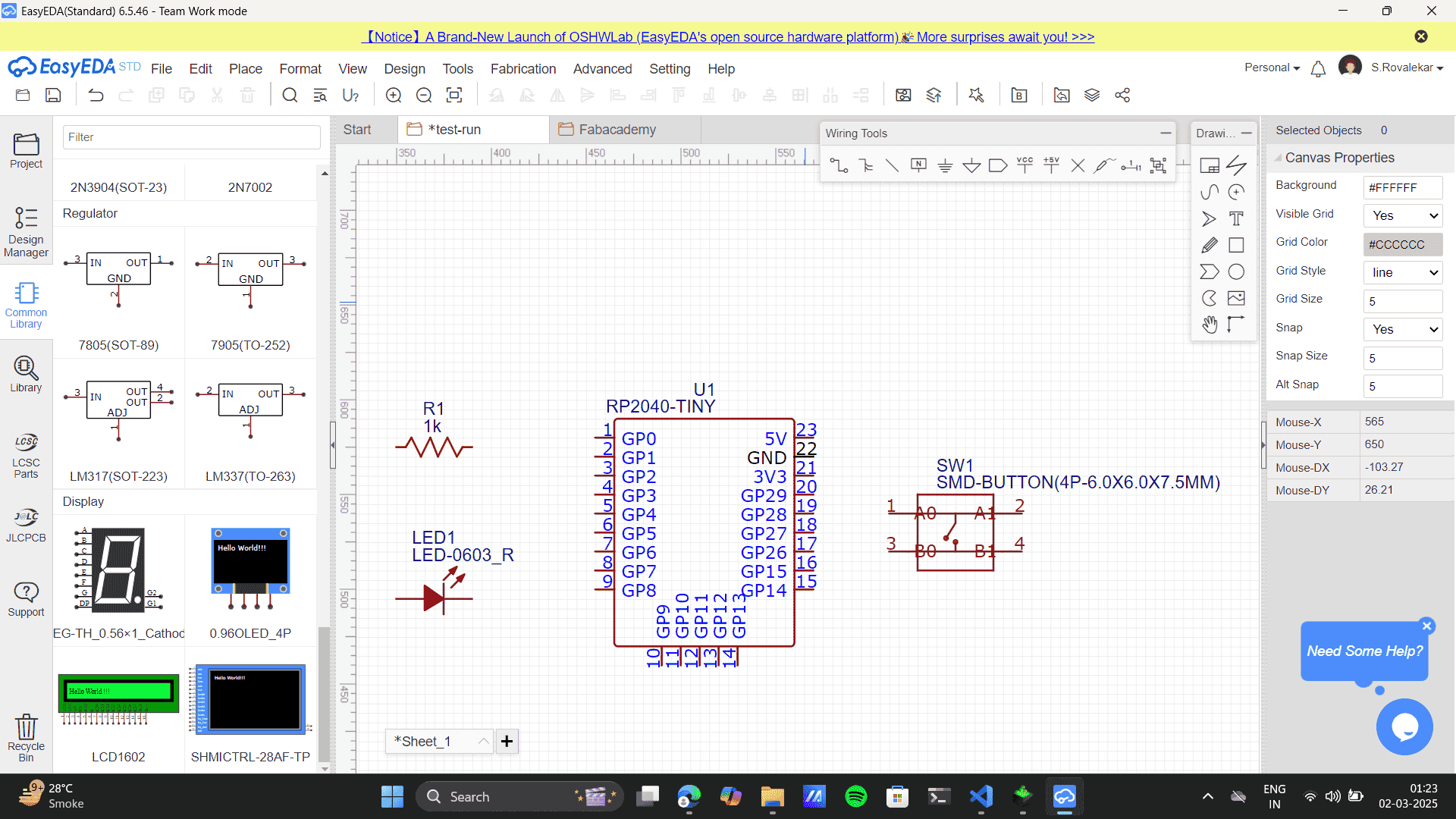
- Step-by-step connecting required pins to the next to build the circuit. Use the "Wire"
tool
to connect components.
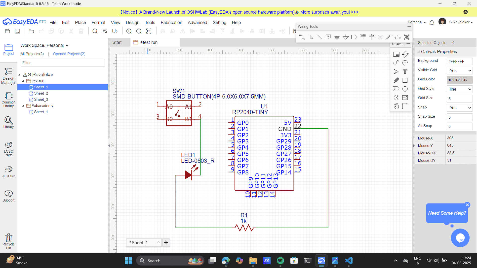
- Final connections

- Taking reference to the wokwi simulation that I built in Week 4 of the Embedded Programming Week
Refer to my documentation,
Embedding Programming to learn my process. I checked the simulation on Wowki.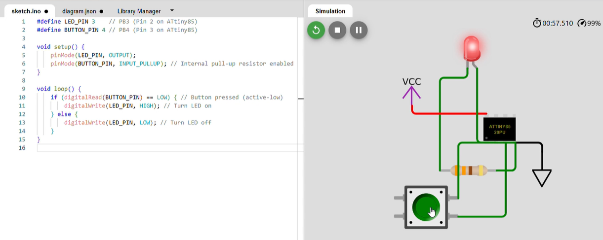
- Clicked "Save" when the circuit was done.
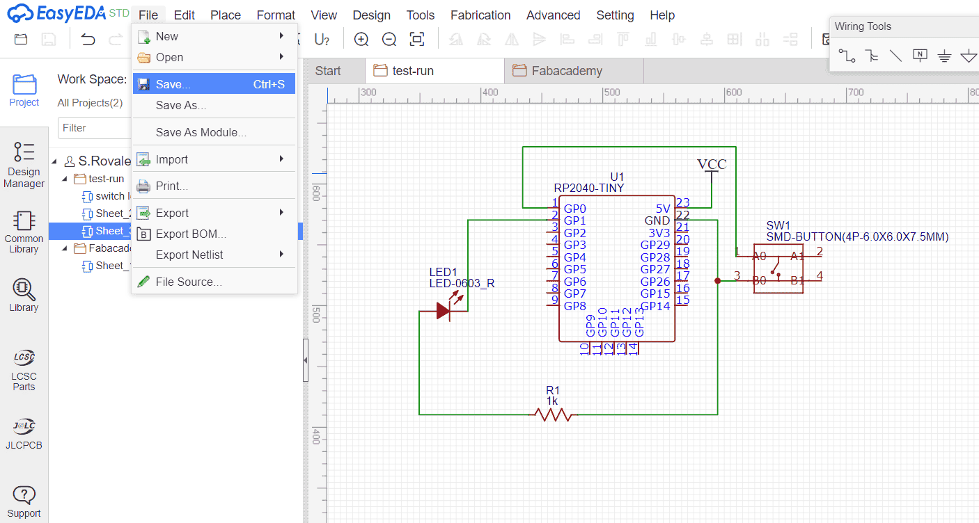
- Now go to Design> Convert to PCB
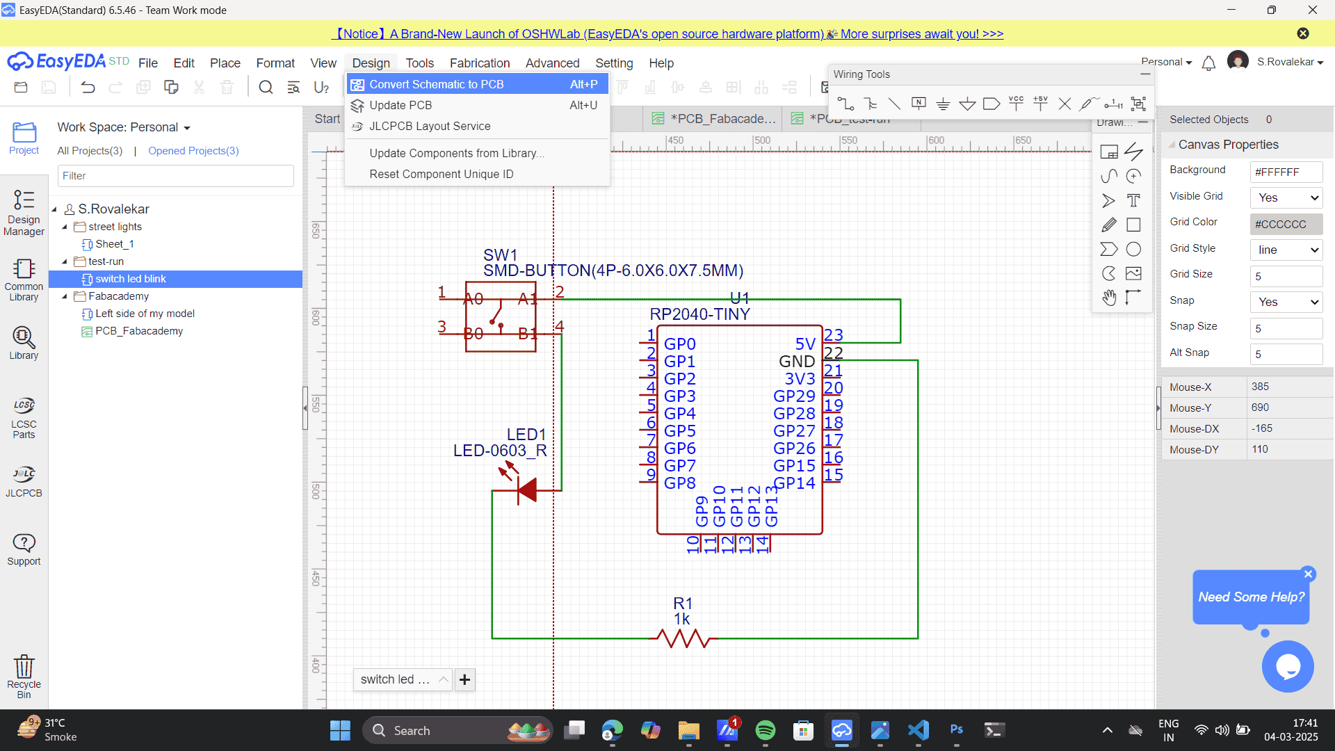
- I set the below settings for building my PCB as default> Set Start X and Start Y as Zero> Apply
.png)
- Drag the PCB to the centre of Board Outline.
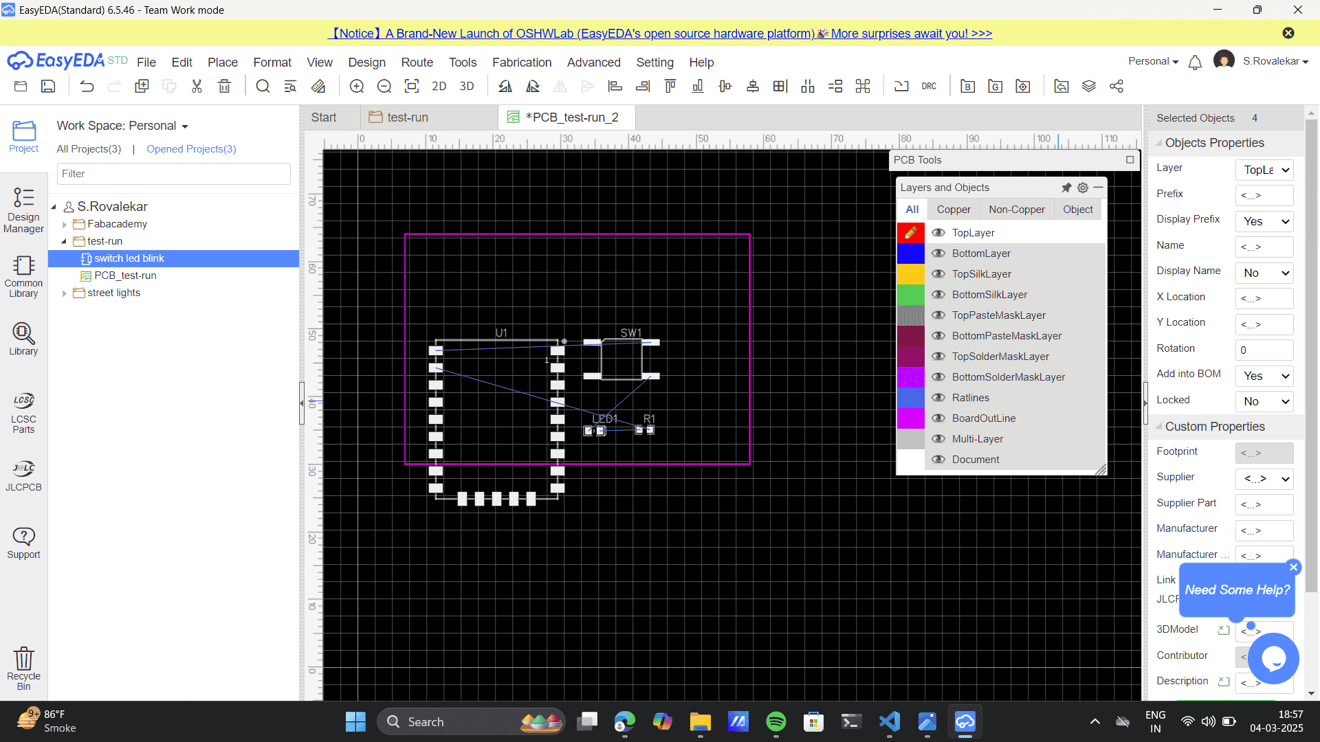
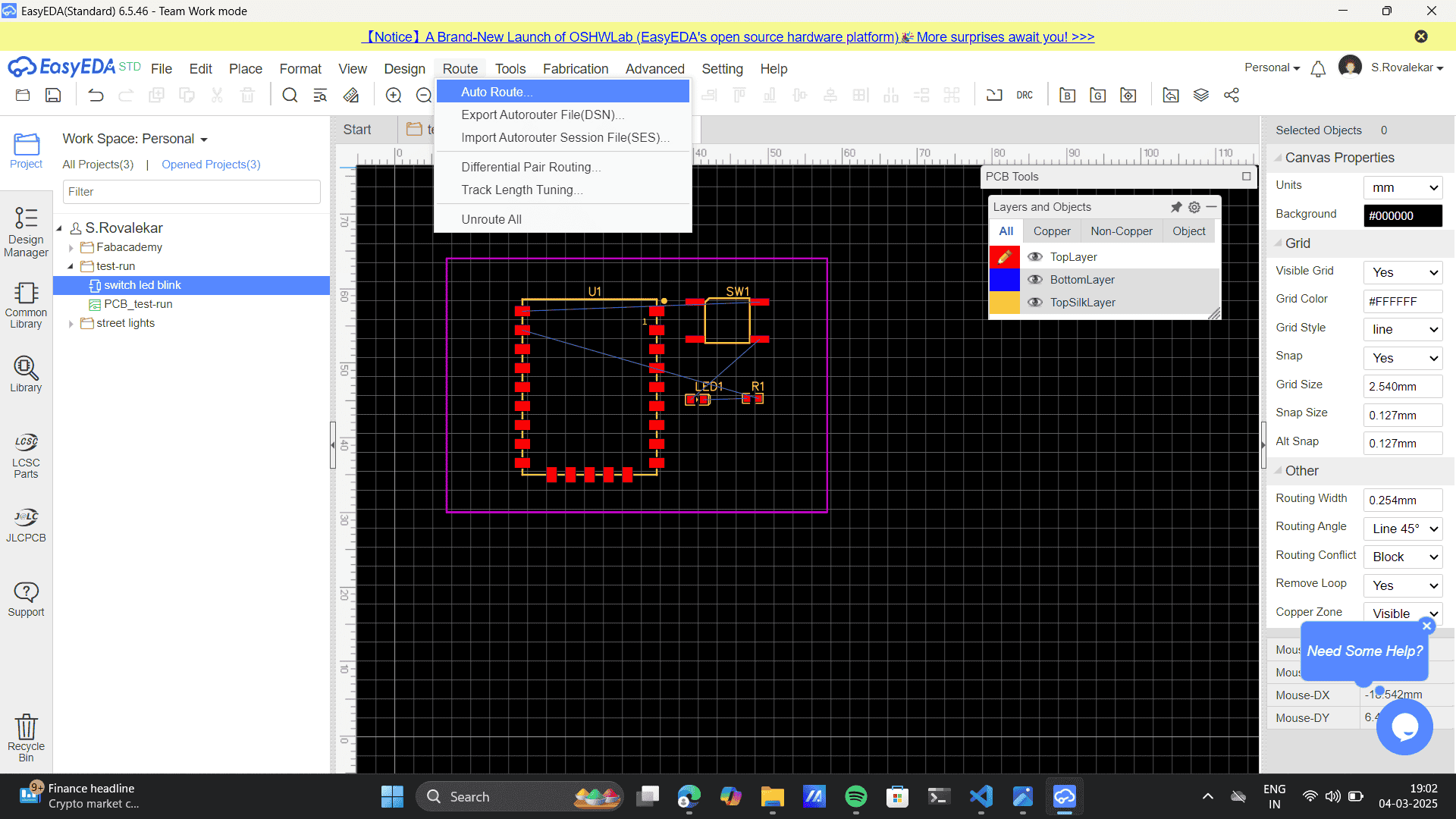
- As the design is not very complex, go to route> auto-route to route the PCB. Routing a PCB (Printed
Circuit Board) refers to the process of designing and laying out the electrical connections (traces)
between components on the board.
Power
Power (P) in electronics refers to the rate at which electrical energy is transferred or converted into another form (such as heat, light, or motion). It is measured in watts (W) and calculated using the formula: 𝑃 = 𝐼 𝑉 P=IV where I is current (amps) and V is voltage (volts). Power is essential for running electronic devices, and it can come from batteries, power supplies, or other energy sources.
Microcontroller & Interfaces
Microcontrollers are compact computing devices that handle both digital and analog tasks, making them essential for embedded systems. They integrate a processor, memory, and input/output (I/O) peripherals on a single chip, allowing them to control various electronic devices efficiently.
Microcontrollers manage digital/analog tasks using GPIO, I2C, SPI, and ADC for communication and peripheral control. In Week 4, of embedded Programming, I worked with the RP2040 microcontroller, a dual-core ARM Cortex-M0+ processor. It features flexible I/O and multiple communication interfaces, making it ideal for real-time applications and embedded projects. Refer to my documentation to learn more about microcontrollers: Embedded Programming.
Peripherals
Peripherals are external or built-in components that allow a microcontroller to interact with the
physical world. They enable data collection, processing, and control of external devices, expanding
the
functionality of an embedded system.
Sensors detect environmental changes, actuators convert electrical signals into movement, and
buttons/switches provide user input. Some of the microcontroller peripherals are:
1. Sensors (Input Peripherals)
Sensors detect environmental changes and convert them into electrical signals for processing by the microcontroller. Refer to my documentation to learn more about Input Devices: Input Devices
Actuators convert electrical signals from the microcontroller into physical actions like motion, sound, or light. Refer to my documentation to learn more about Output Devices: Output Devices
These allow users to manually provide input to the microcontroller.
Circuits & Design
Electrical circuits function based on three fundamental parameters: current (A), voltage (V), and power (P). Electrical circuits operate on current (A), voltage (V), and power (P = I²R = IV). Electrical circuits function based on three fundamental parameters: current (A), voltage (V), and power (P). Voltage (V) is the electrical potential difference that pushes electrons through a circuit, similar to water pressure in a pipe. Current (A) is the flow of electric charge, determining how much electricity moves through a circuit. Power (P), given by formulas like P = IV and P = I²R, represents the rate at which electrical energy is consumed or transferred within a circuit.
Kirchhoff’s Laws – The Foundation of Circuit Analysis1. Kirchhoff’s Current Law (KCL)
This law states that the sum of all currents entering a node (junction) is equal to the sum of all currents leaving the node. It ensures that charge is conserved, meaning no extra charge accumulates at a junction. Example: In a parallel circuit, the current splits into different branches, but the total entering and leaving remains the same.
2. Kirchhoff’s Voltage Law (KVL)This law states that the sum of voltages around a closed loop is always zero. It means that the energy supplied by sources (like batteries) is completely used up by components (like resistors, LEDs, etc.). Example: In a simple series circuit with a battery and resistors, the voltage drops across each resistor add up to the total voltage supplied by the battery.
.png)
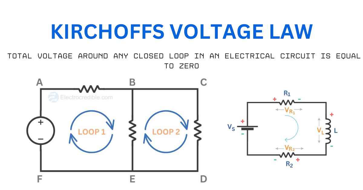
Understanding these laws helps in circuit design, troubleshooting, and optimization. These concepts form the foundation of circuit design and debugging, enabling engineers to create stable and efficient electronic systems.
EDA Tools
Electronic Design Automation (EDA) tools are essential for designing and simulating electronic circuits. Software like KiCad, Eagle, Altium, and EasyEDA assist engineers in creating schematics, placing components, routing traces, and generating PCB layouts. These tools automate complex design processes, ensuring efficient circuit board design while following electrical and manufacturing constraints. Advanced features include auto-routing, design rule checks (DRC), and 3D visualization, making them indispensable for both professionals and hobbyists working on custom electronic projects. I will be using the EasyEDA for designing and simulating my electronic circuit. Check my further documentation to got trhought the whole process.
PCB Design
Designing a Printed Circuit Board (PCB) involves several key steps to ensure functionality and manufacturability. The process includes placing components, routing electrical traces, and defining layers to create a compact and efficient layout, as we can do using the EDA tools for building the schematics. To prevent design errors, tools like Design Rule Check (DRC) and Electrical Rule Check (ERC) are used to verify proper spacing, trace widths, and electrical connections. A well-designed PCB improves circuit performance, reduces noise, and enhances reliability in electronic systems.
Simulation & Testing
Simulation & Testing are essential steps in electronic circuit design to verify functionality before physical implementation. Simulation uses software to model circuit behavior under different conditions, helping to detect errors and optimize performance. Testing involves using hardware tools like oscilloscopes, multimeters, logic analyzers, and function generators to measure voltage, current, and signal integrity in real circuits.
SimulationFalstad, Wokwi, and EveryCircuit are interactive simulation tools that allow users to visually design and test electronic circuits in a user-friendly environment. They provide real-time feedback, making them great for beginners and professionals to understand circuit behavior without physical components. In Week 4, of embedded Programming, I worked with the Wokwi, an interactive simulation tools. Refer to my documentation to learn more about my Wowki software usage: Embedded Programming.
Test EquipmentERC (Electrical Rule Check) vs. DRC (Design Rule Check)
Some terms I learnt during the process were DRC and ERC.
Both are essential for error-free PCB or IC design.
ERC ensures the circuit functions electrically correct.
DRC ensures the design is physically manufacturable.
| Feature | ERC (Electrical Rule Check) | DRC (Design Rule Check) |
|---|---|---|
| Purpose | Checks for electrical connectivity and logic errors. | Ensures physical design follows fabrication constraints. |
| Focus | Electrical issues like open nets, short circuits, incorrect pin connections, missing power/ground connections. | Geometric constraints like spacing, width, overlaps, via sizes, and layer rules. |
| Scope | Logical and connectivity-based errors. | Physical layout errors. |
| Used In | Schematic design (before PCB layout). | PCB layout and IC design. |
| Example Errors | Floating pins, incorrect net connections, power/ground issues. | Track width violations, spacing violations, overlapping traces. |
Exploring the software: EasyEDA
EasyEDA is a free, web-based Electronic Design Automation (EDA) tool used for designing schematics, PCB layouts, and circuit simulations. It provides a user-friendly interface for hobbyists, students, and professional engineers to create and test electronic circuits online.
Key Features of EasyEDA:EasyEDA Step-by-Step Guide
Step 1: Sign Up & Log In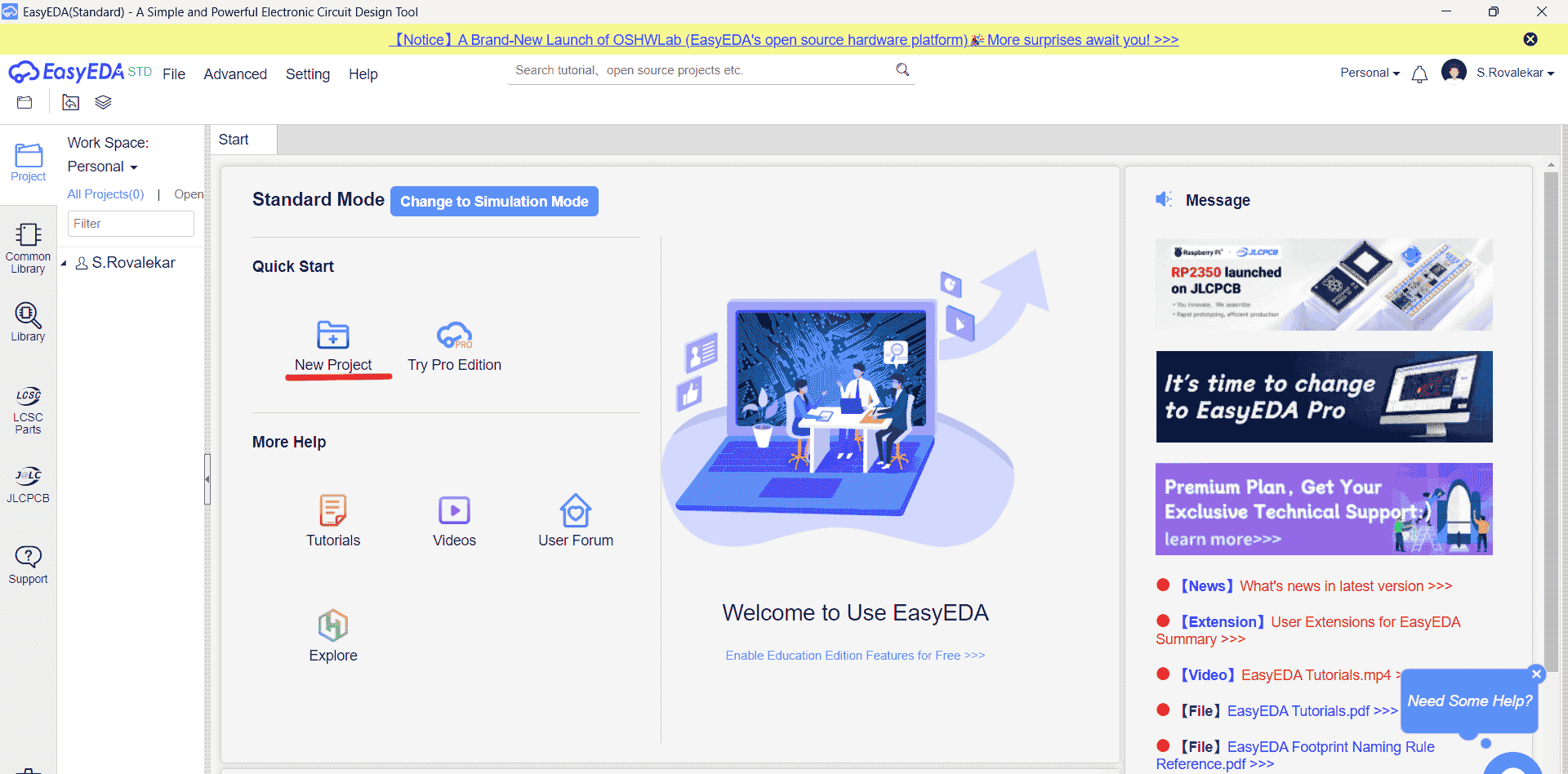
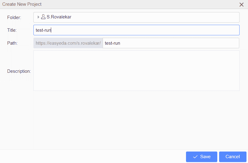
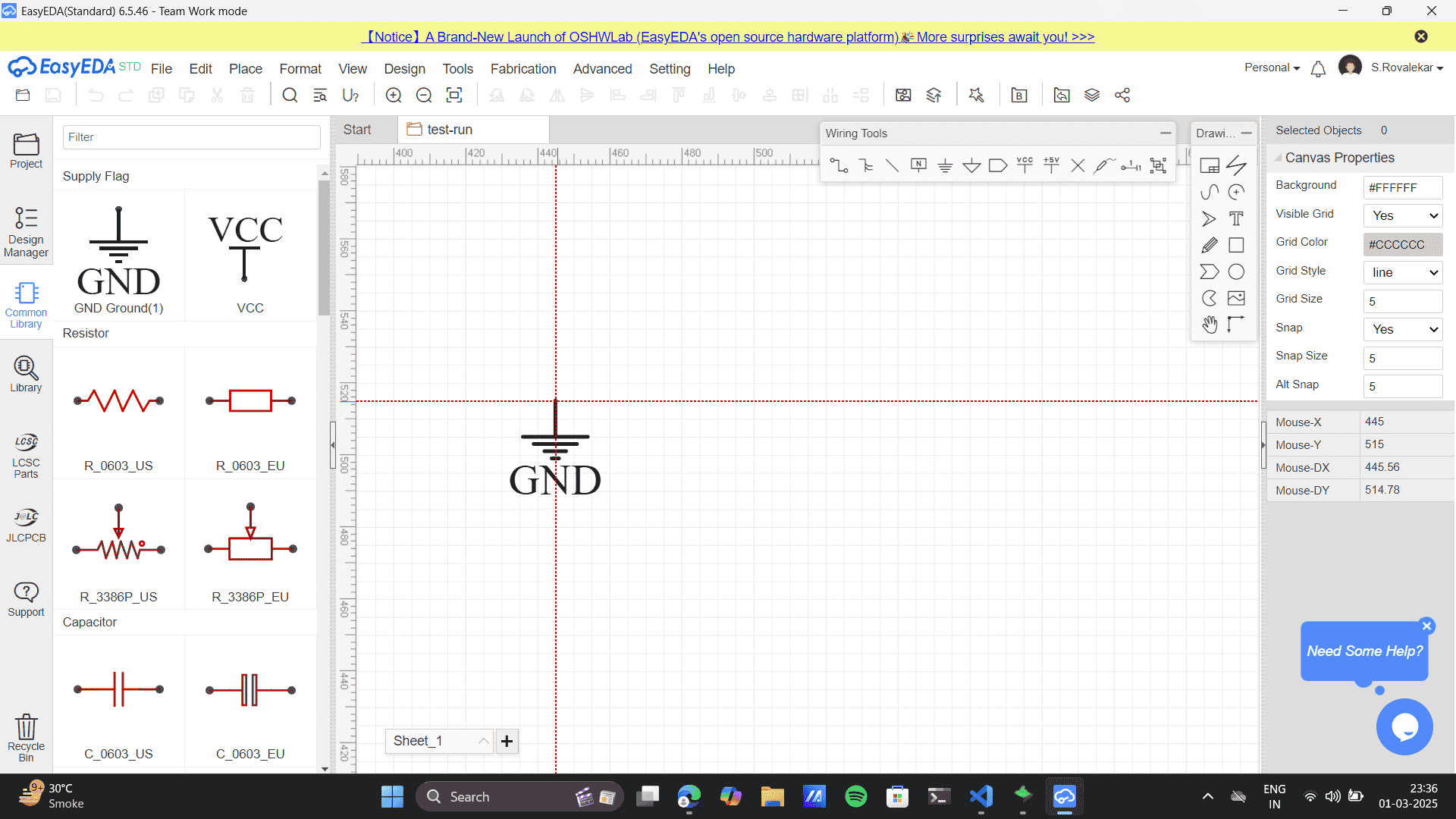
The interface displaying the Library panel, where users can search for electronic components to use in their circuit design. It has a Filter Features in the Library Panel. The understanding of the filter components was a little complex for me, thus I break down thte description for my understanding.
Building Schematic to PCB
As the circuit is short, I selected only the top layer in the configure layers. The Top Layer in PCB design is the uppermost copper layer where components and traces are placed. It is used for routing signals, power, and ground connections.
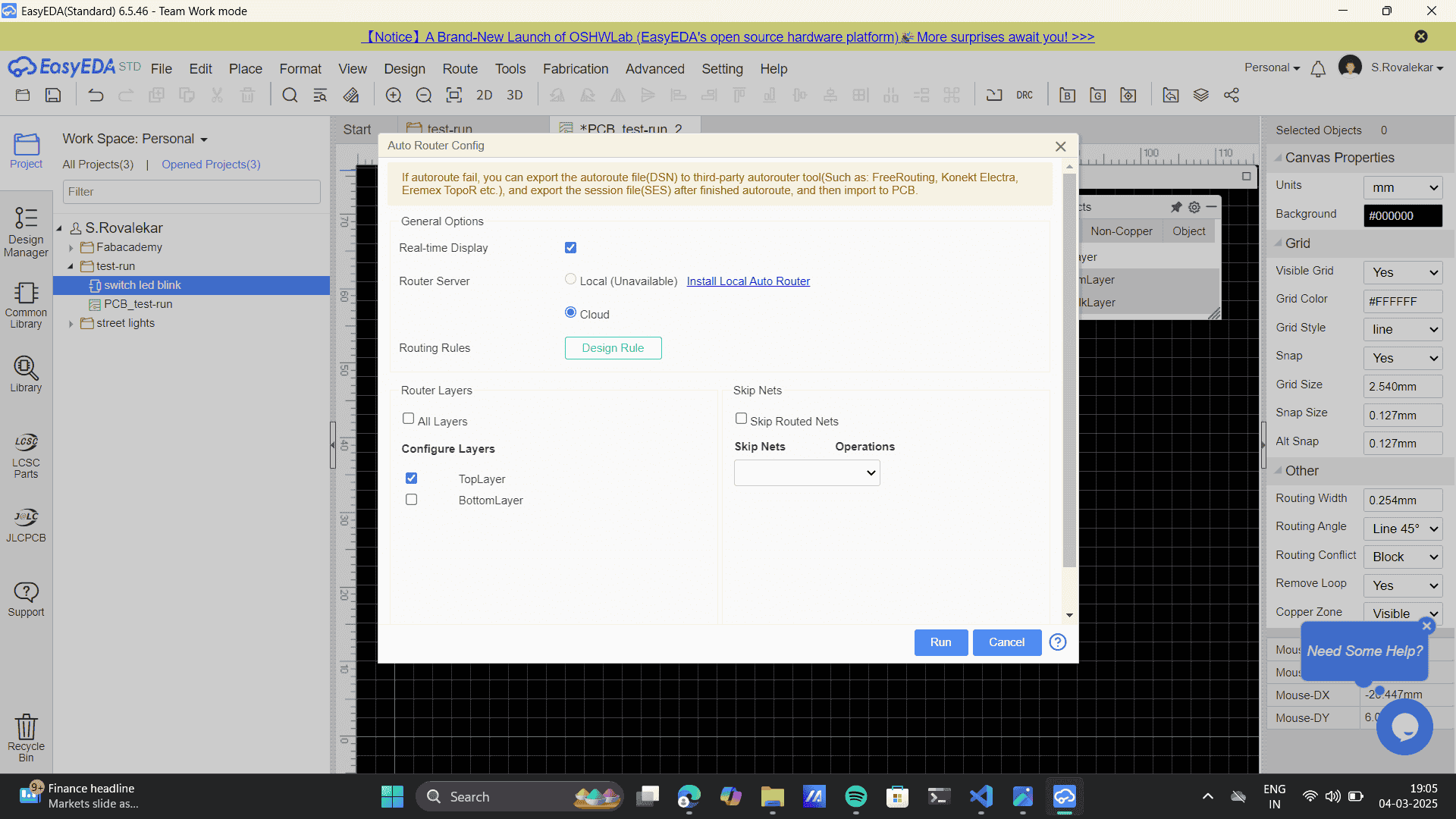
As the design is not very complex, thus go to route> auto-route to route the PCB

Auto route configuration panel appears> untick bottom layer> Apply
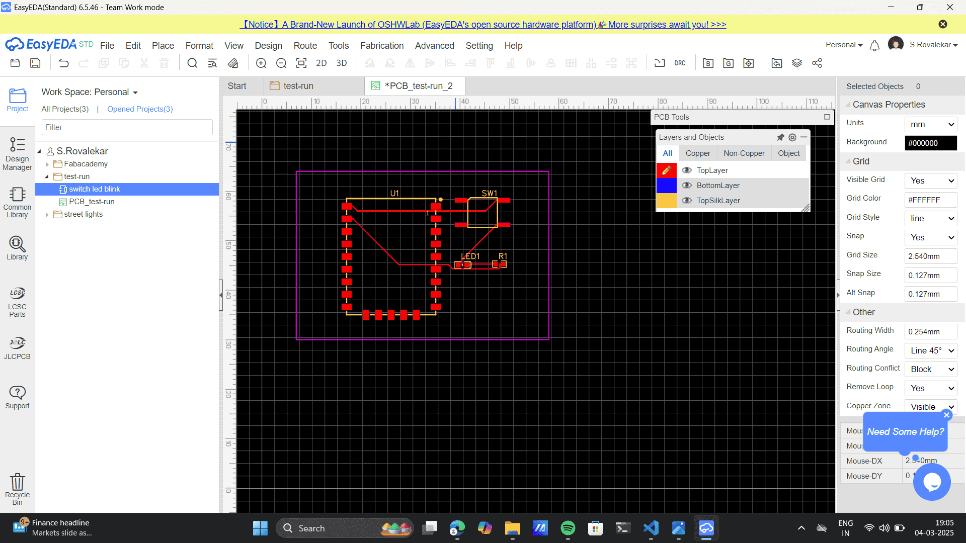
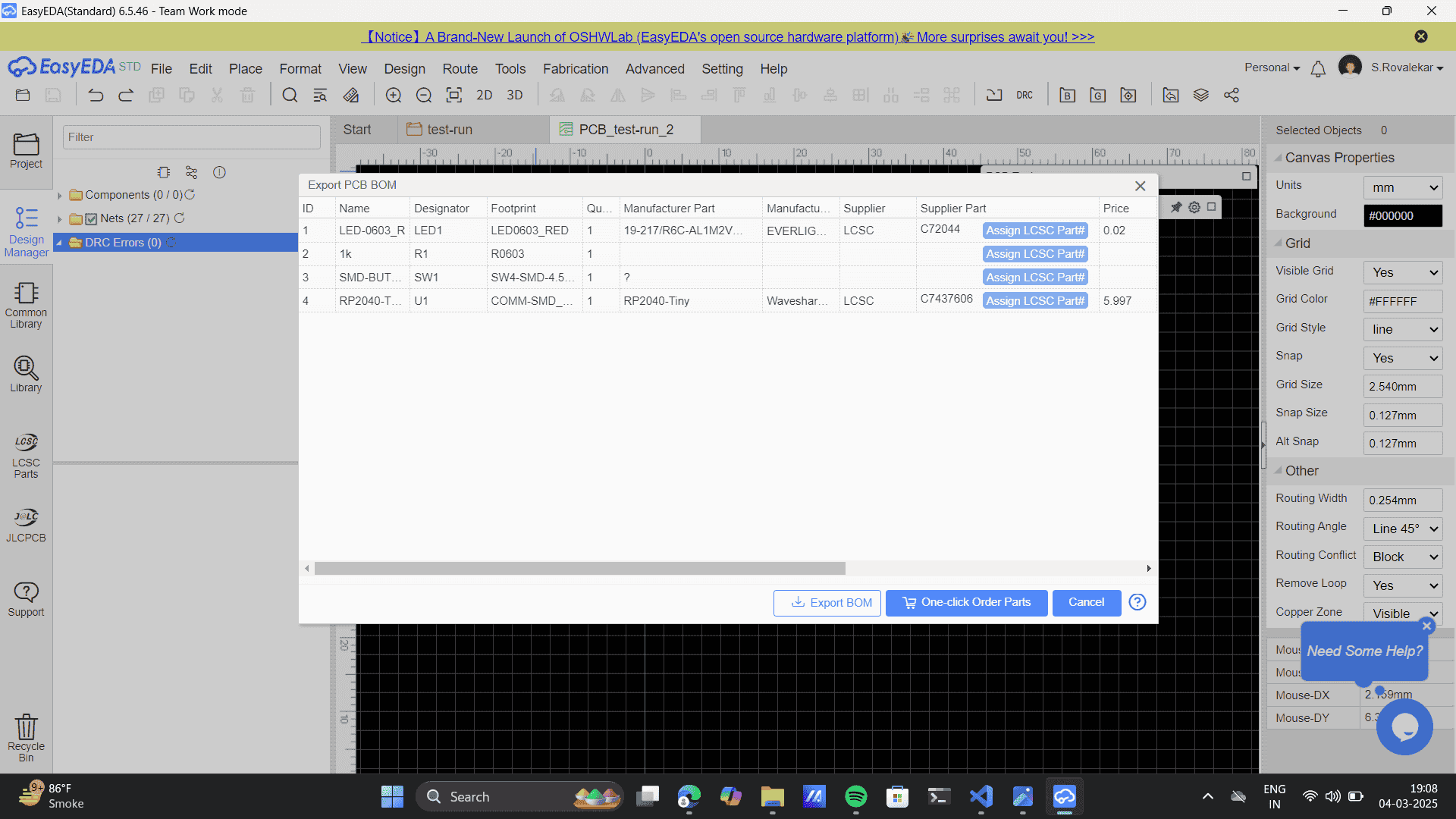
When the PCB is ready select Fabrication> BOM (Bill of materials)

This will give the exact list of materials required for the PCB production
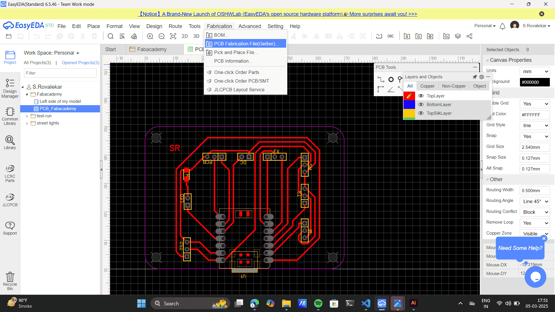
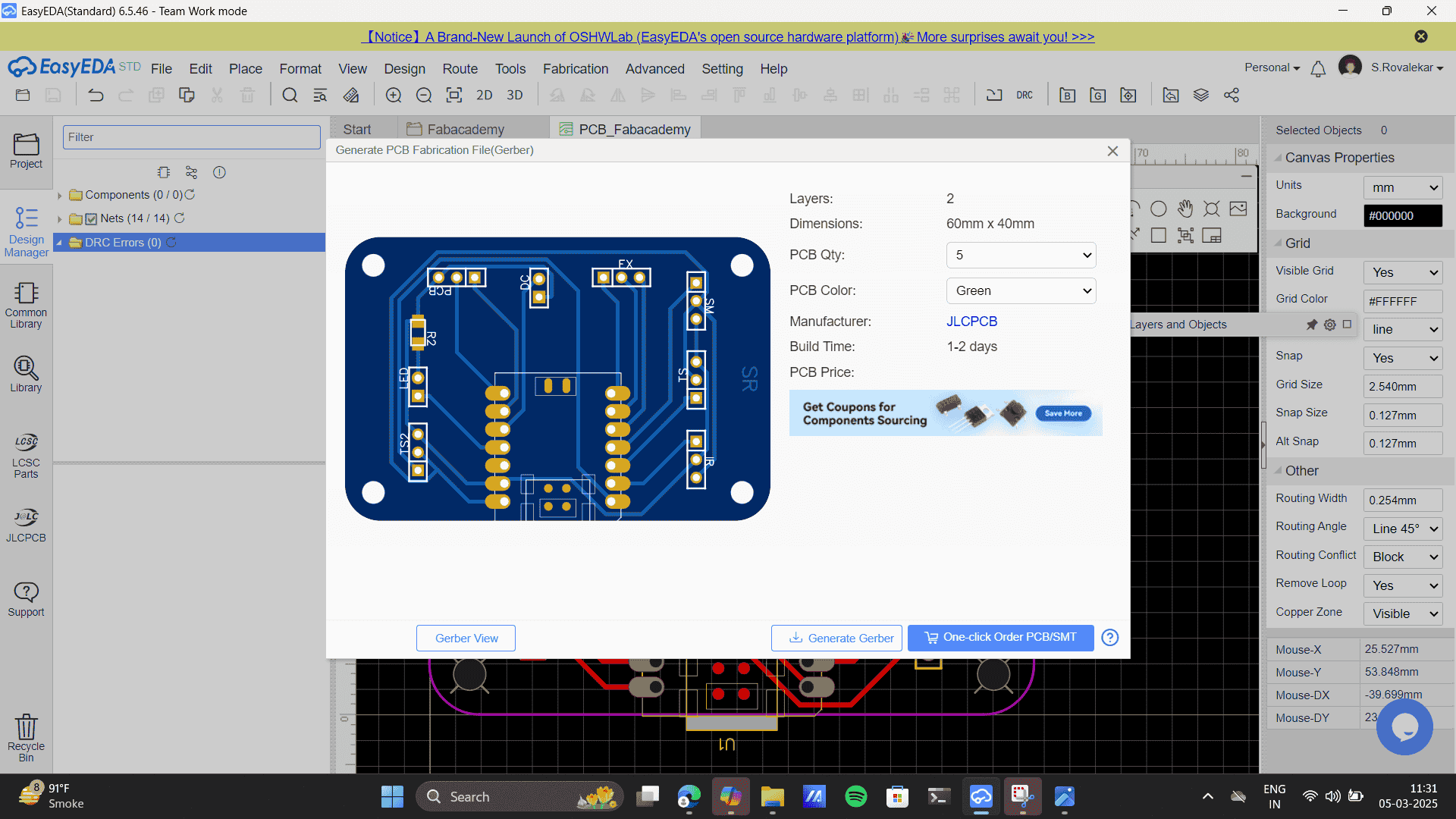
Finally, Fabrication> PCB Fabrication File (Gerber File)
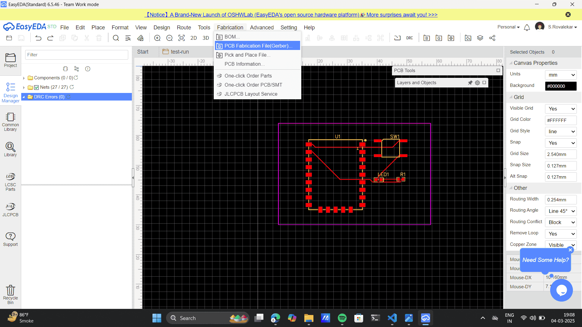
Generate, the Gerber file, ready for production
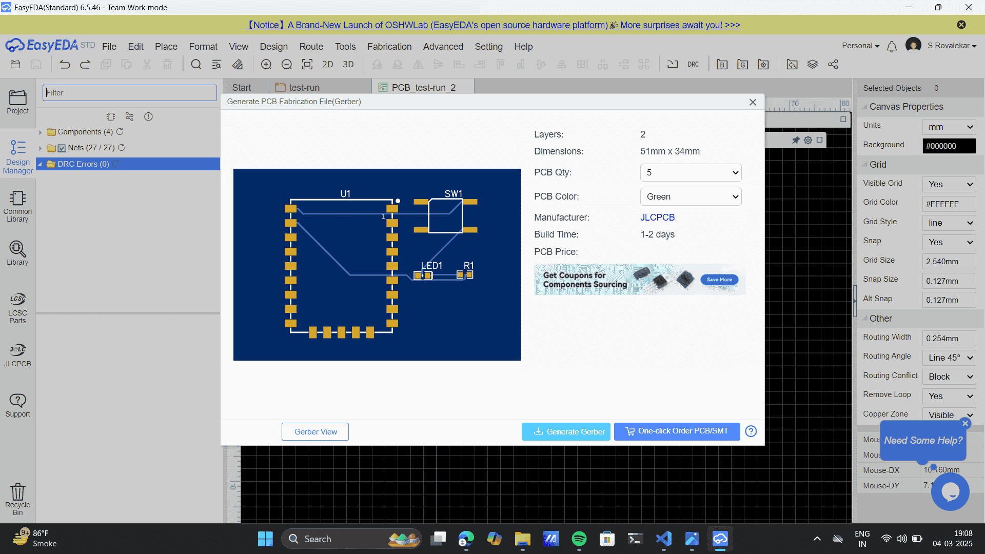
Final Project PCB Design
After understanding the basics of EasyEDA, I went forward with challenging myself to Design and
build
a circuit that could potentially be used for my final project model of the book nook. Attatching the
image
and basic sketch diagram
to analyse its input and output.I used, Touch Sensor and IR sensor for input.
LED indicators for feedback.
DC Motor and Servo Motor as output components.
Diodes and Resistors for protection and control.
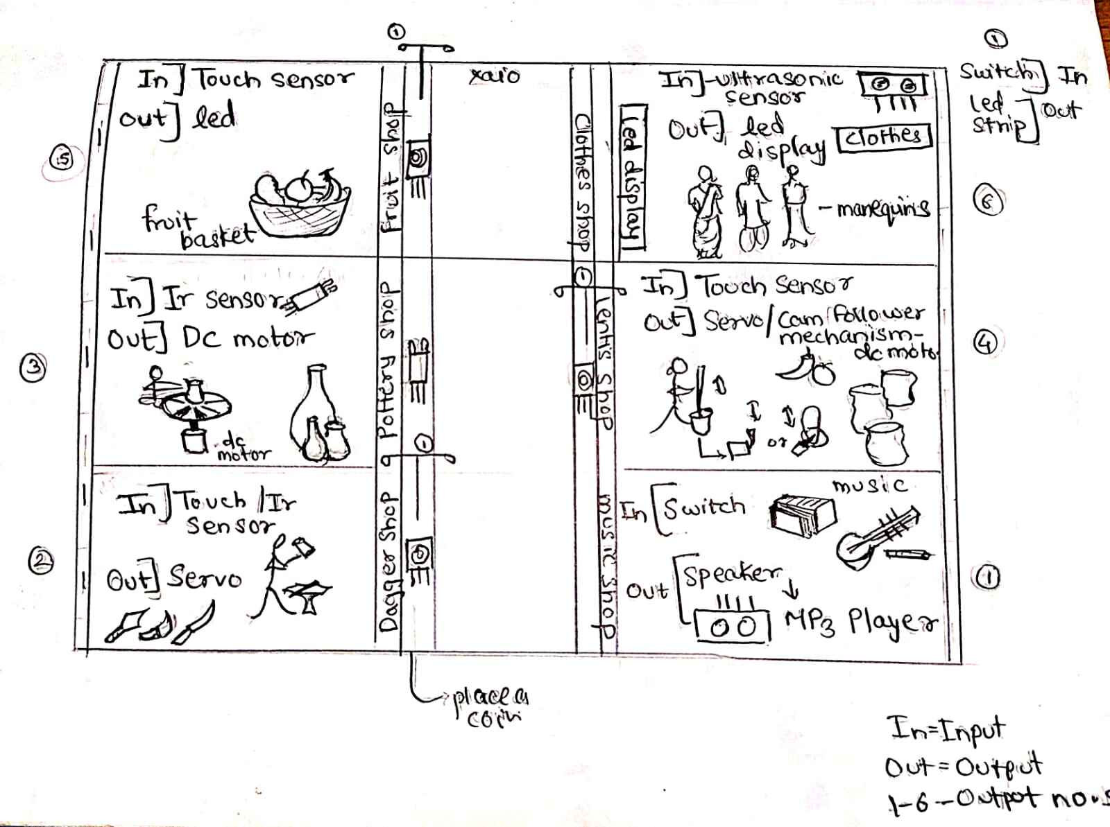
Keeping in mind the sketch for the final project, I build circuit that would function of the half of my overall model. I built a hand-drawn sketch to simplify the understanding of my circuitry.
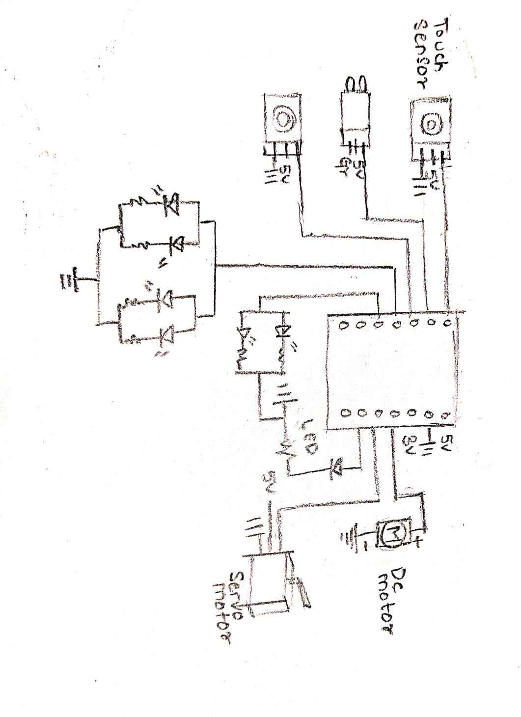
One referring to my on paper sketch I came to the EasyEDA software, to build my circuit for production. Transitioning from a hand-drawn circuit sketch to a professional PCB design using EasyEDA, Here’s a structured approach to building a circuit in EasyEDA:
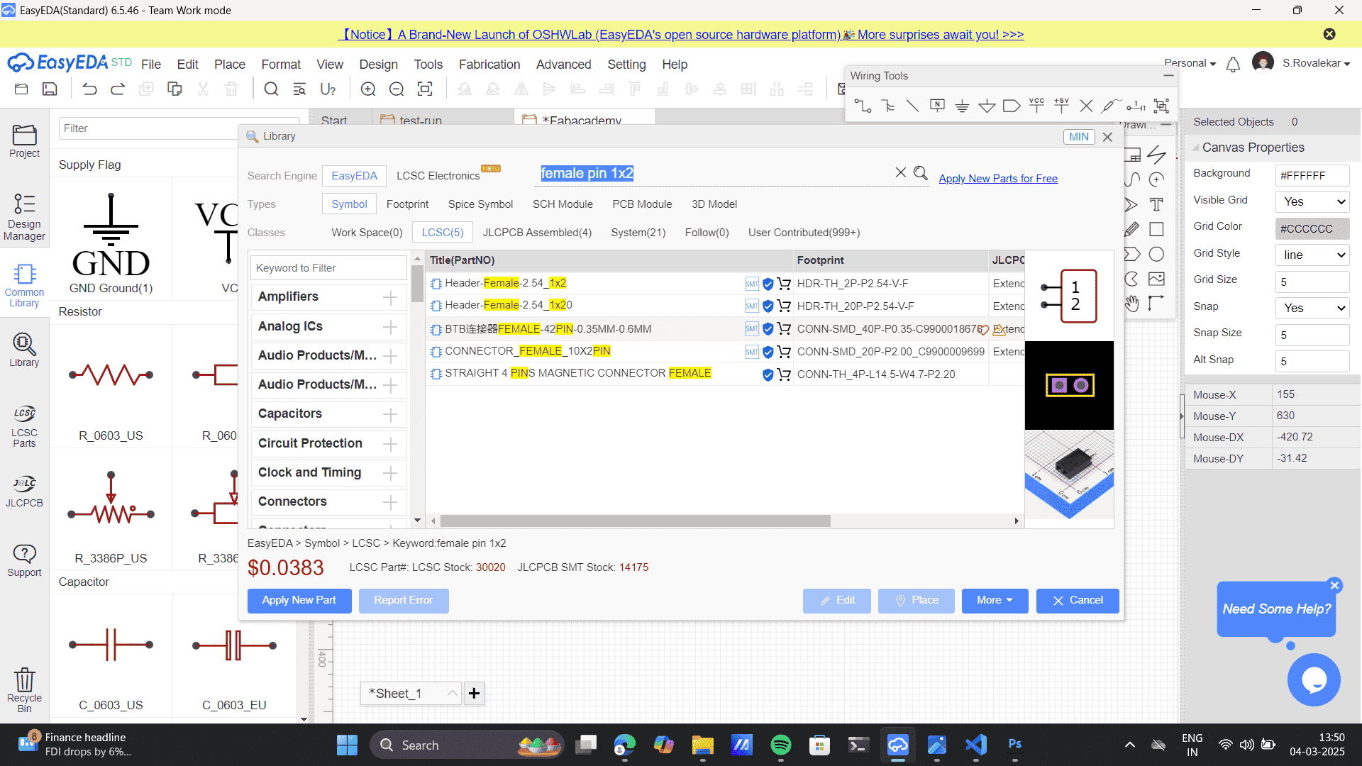
Common library> Female pin 1*2
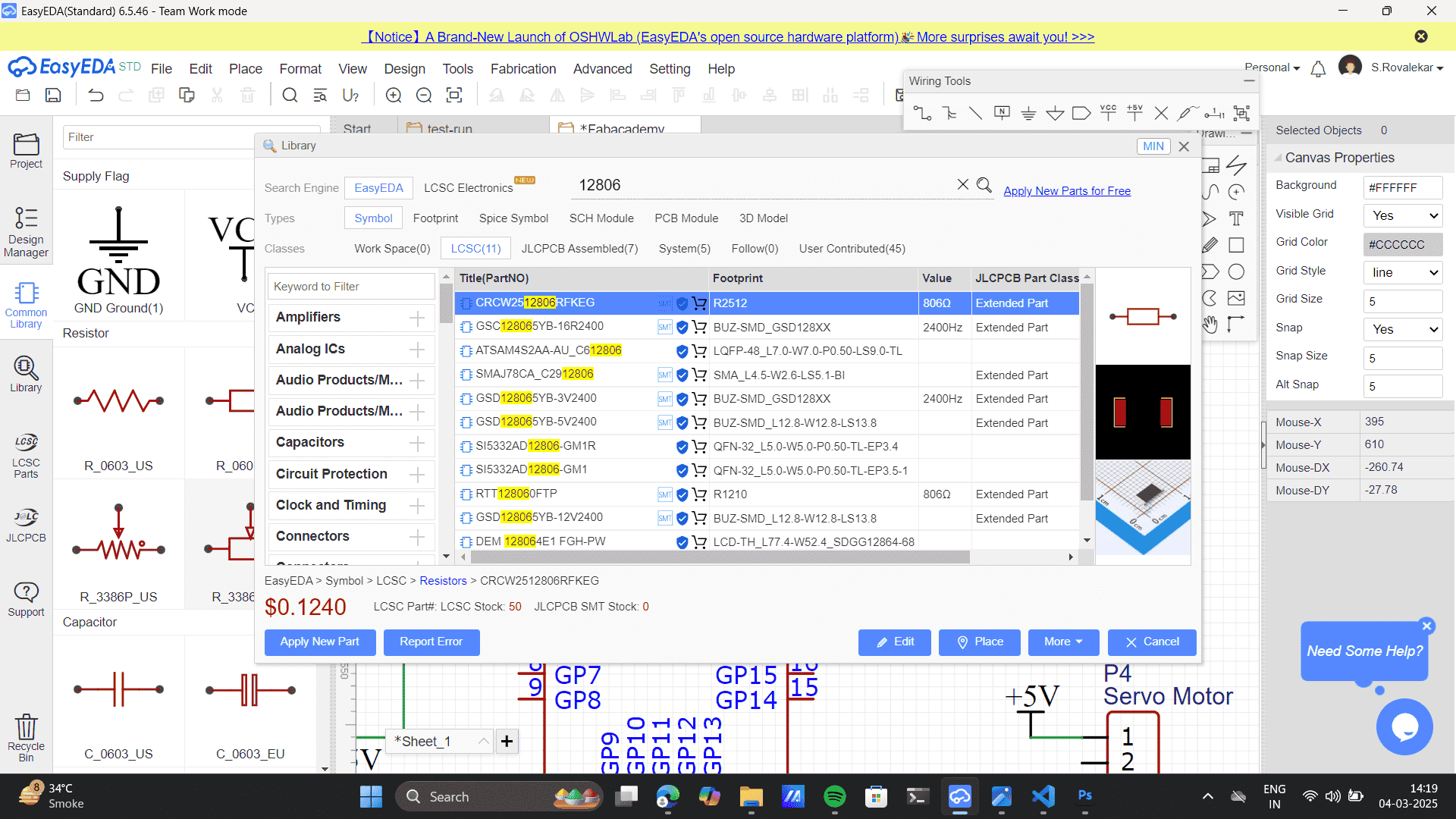
Common library> Resistor 12806
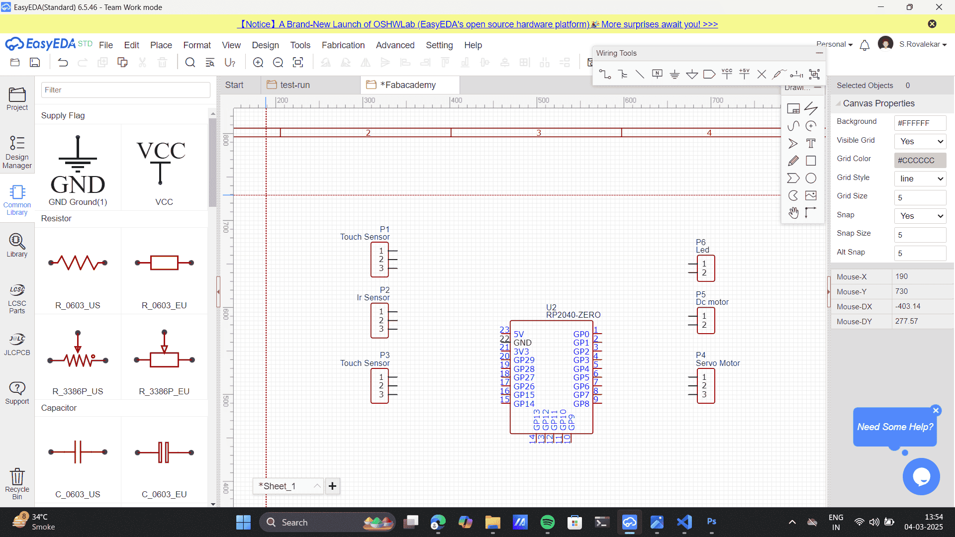
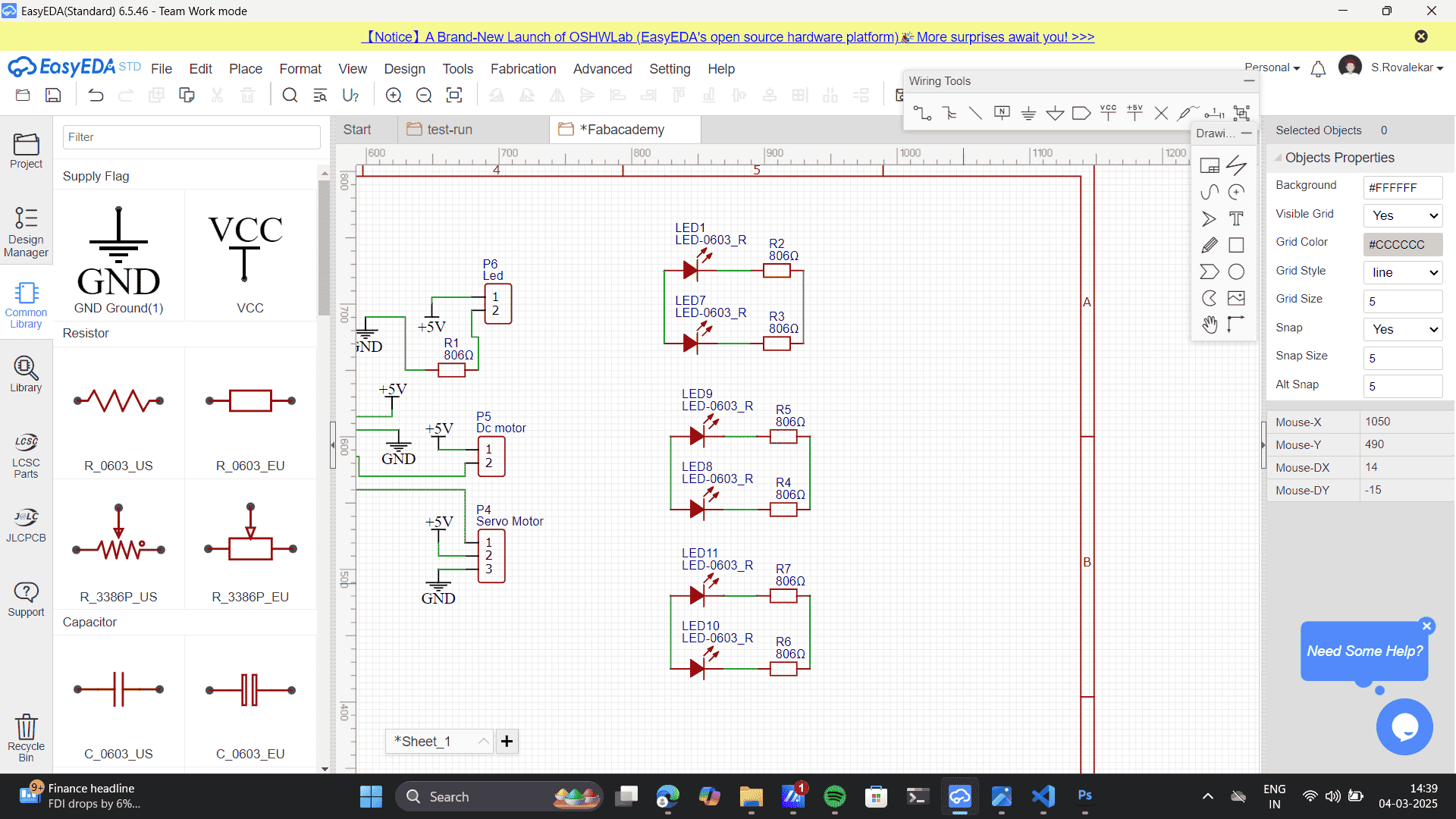
Adding Components from the common library to the sheet.
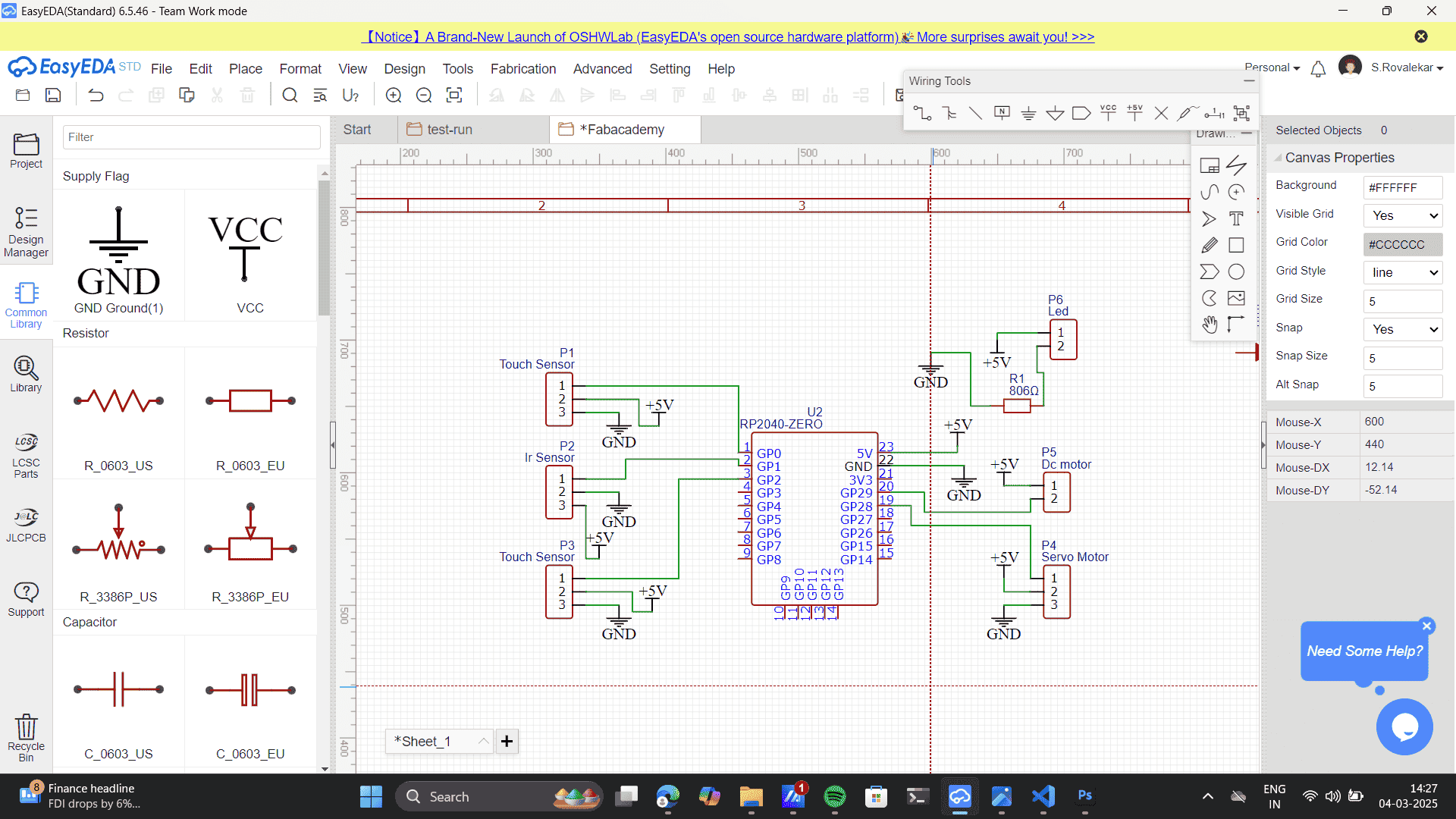
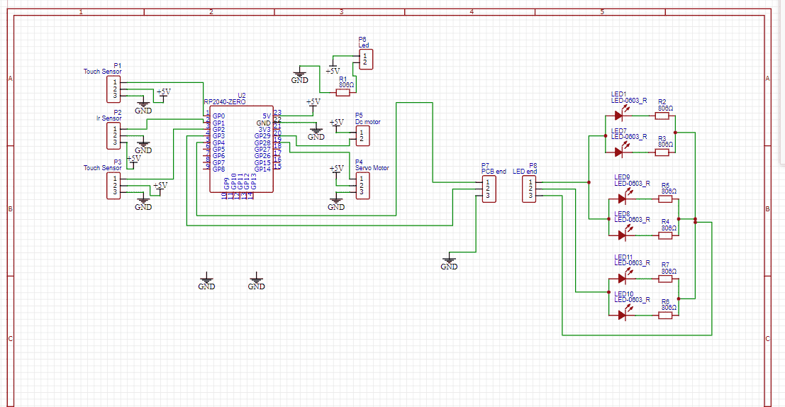
Connecting components to build sketch circuit as above, using the wire connector. I referred to the above sketched schematic for connecting circuit pins.
As per my Model design, My final model consists of 6 led output at a distance, for which I I built an LED circuit to build a second PCB.
Complete circuit.
Design> Convert schemation to PCB
.png)
Drag Values
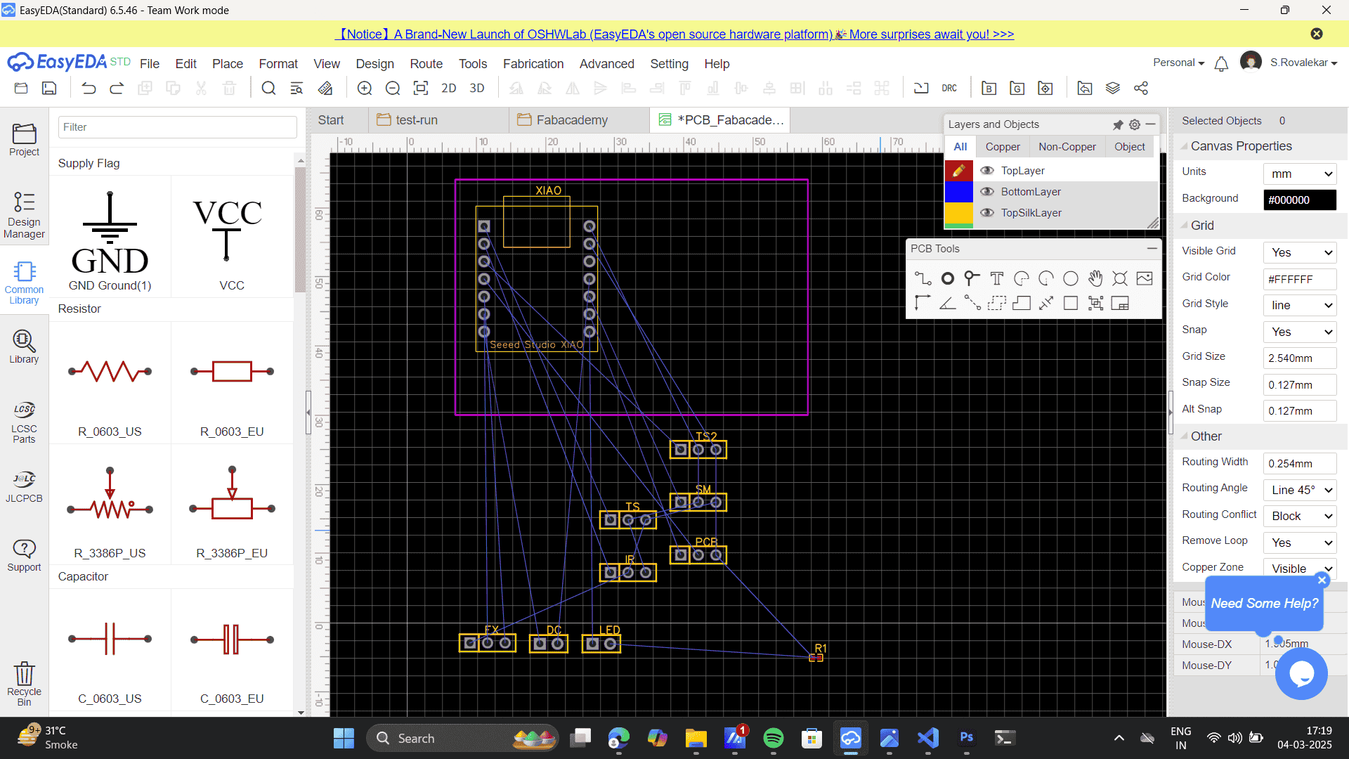
Place the components
Route> Auto-route
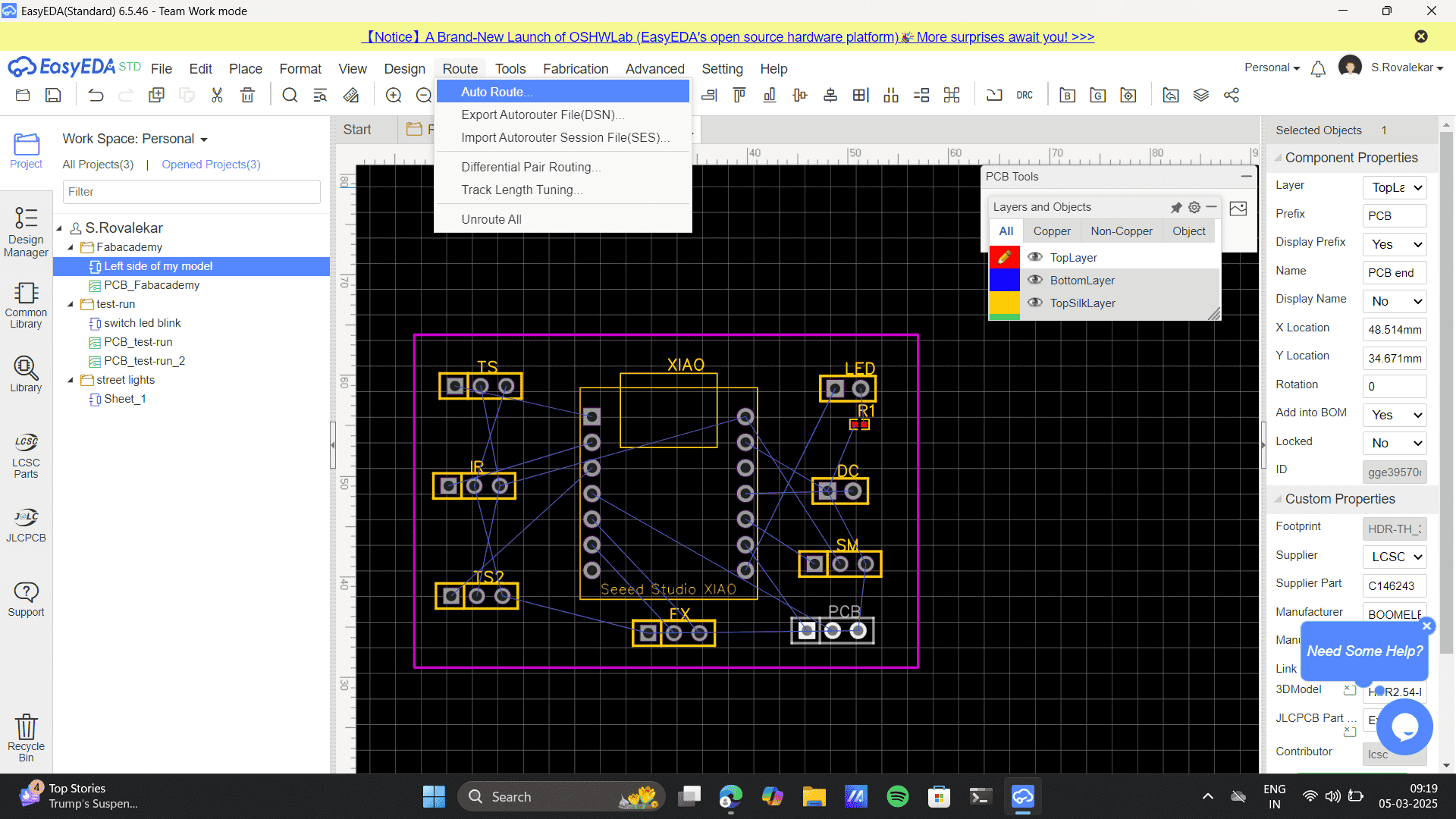
Design rule
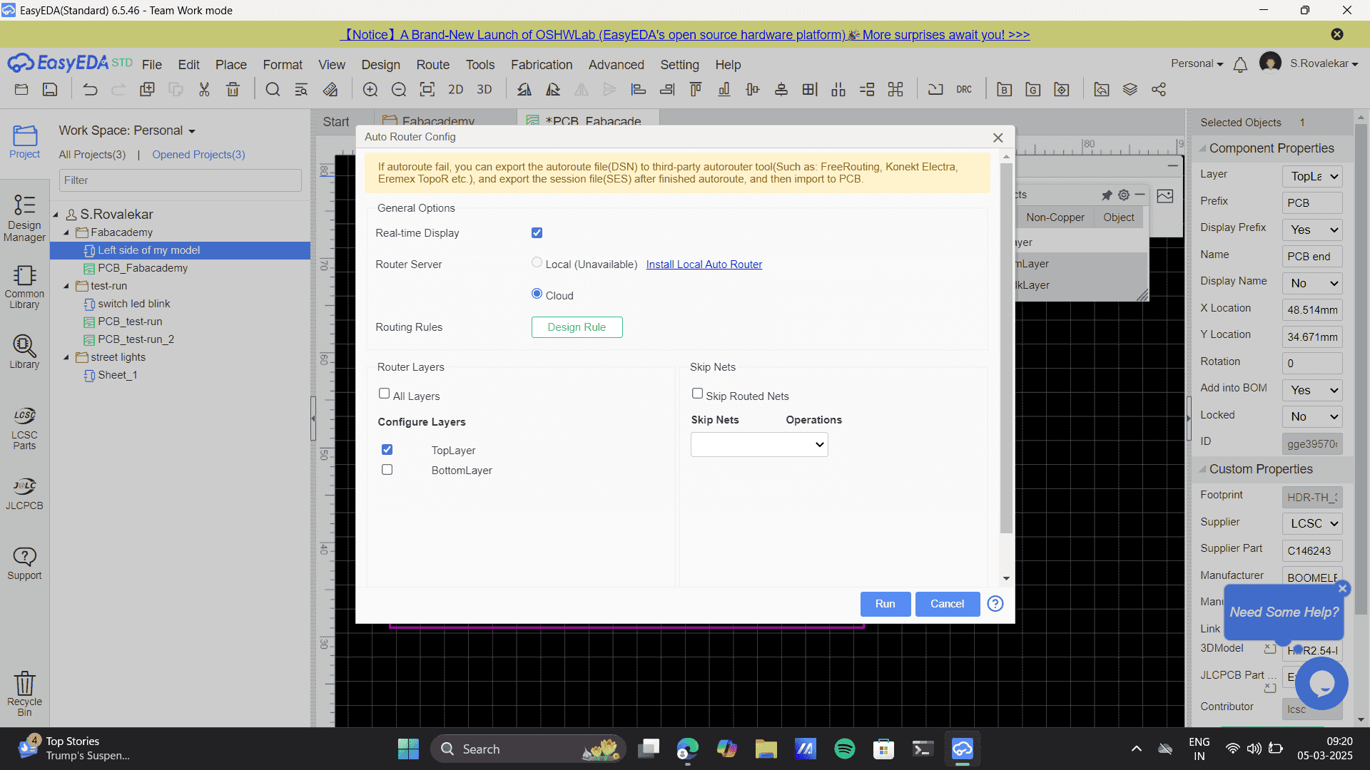
Set track width> set clearance.
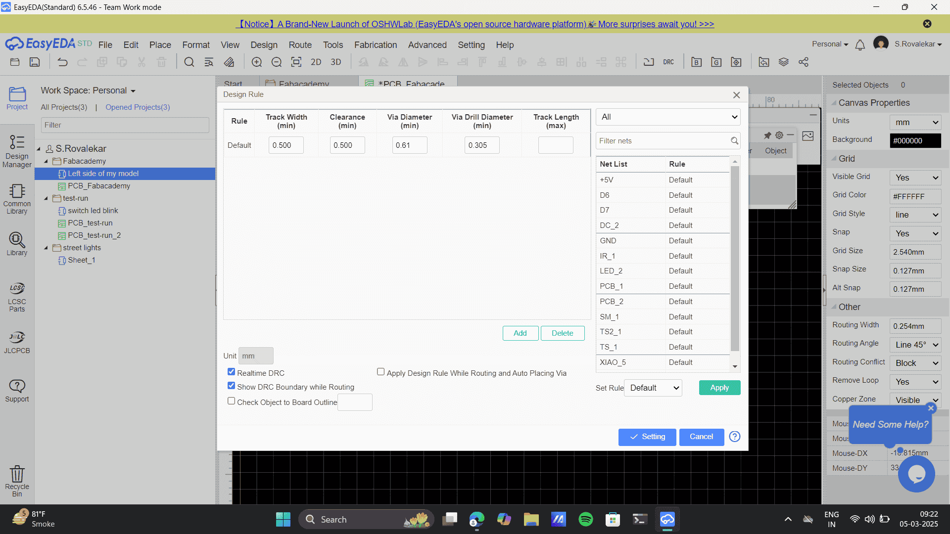

Apply> settings> error
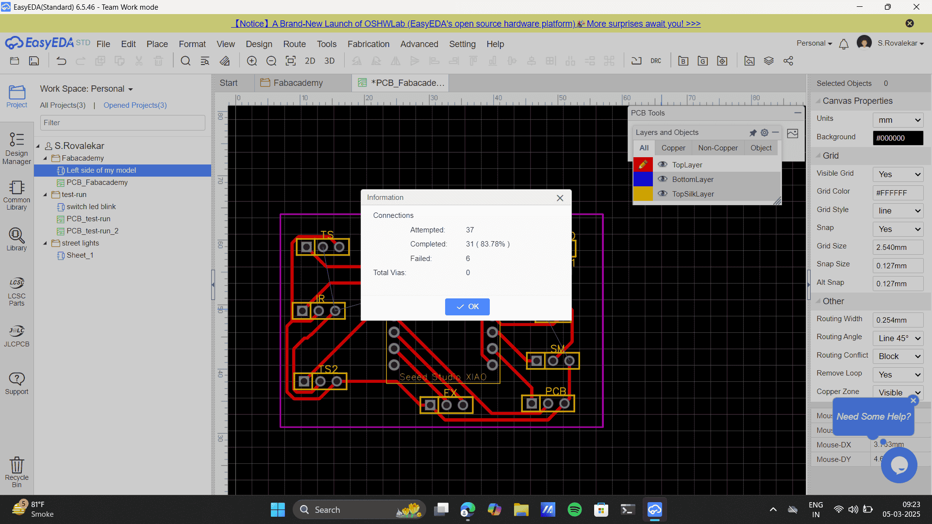
6 connections failed.
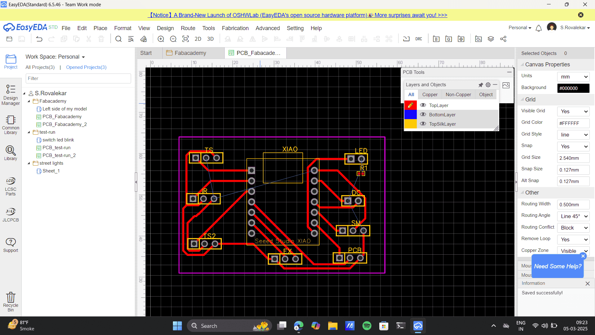
Error attacked. As per the components layout on the board, on auto routing the DRC failed to route 6 connections. So I tried to Change components placements, assembly and rotate components and also changing board size.
Learnings: During the process I learnt that the Xiao Rp2040 I used was incorrect.
Thus, I went to the Library and replaced the Xiao this time from the User contributed setup.
After placing the newly added Xiao, I deleted the previous one and re-wired each connection.
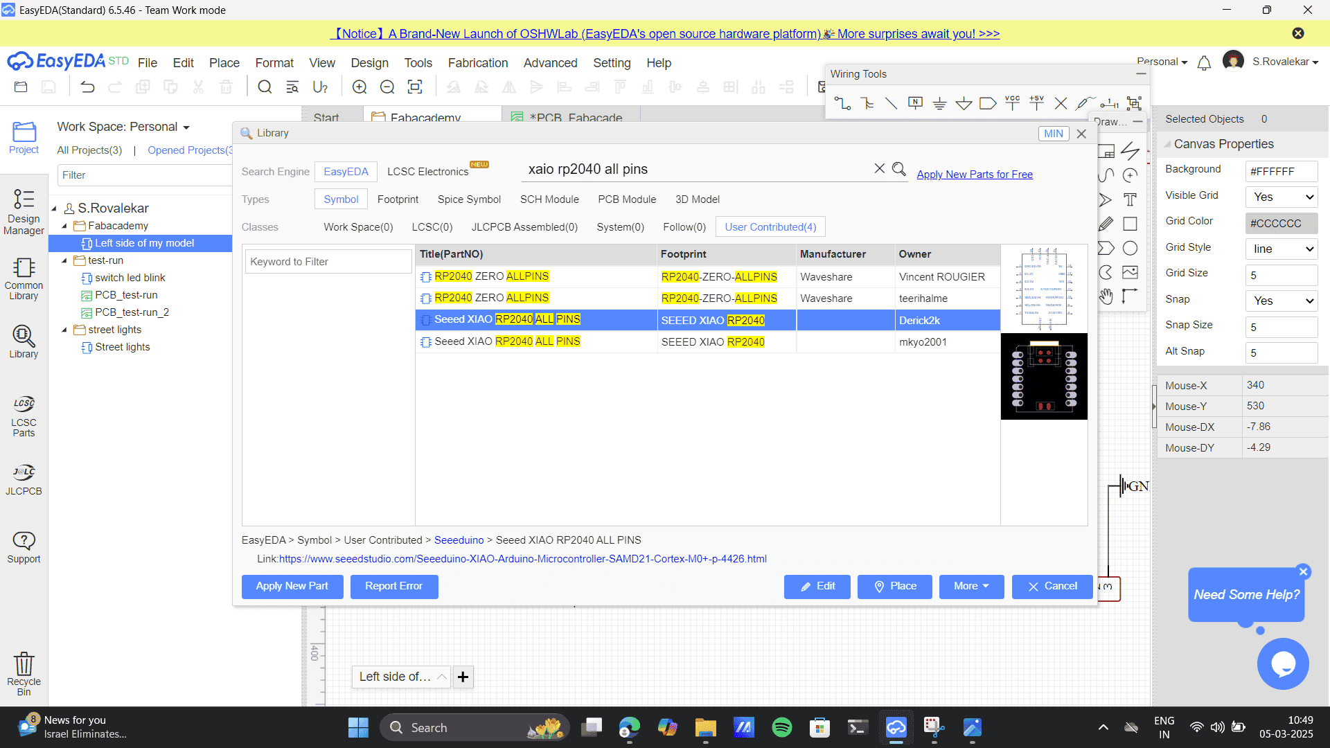
Going back to my DRC errors, I Changed the circuit schematic configuration first, to help me change the configuration on the pcb schematic.
Change components placements, assembly and rotate components
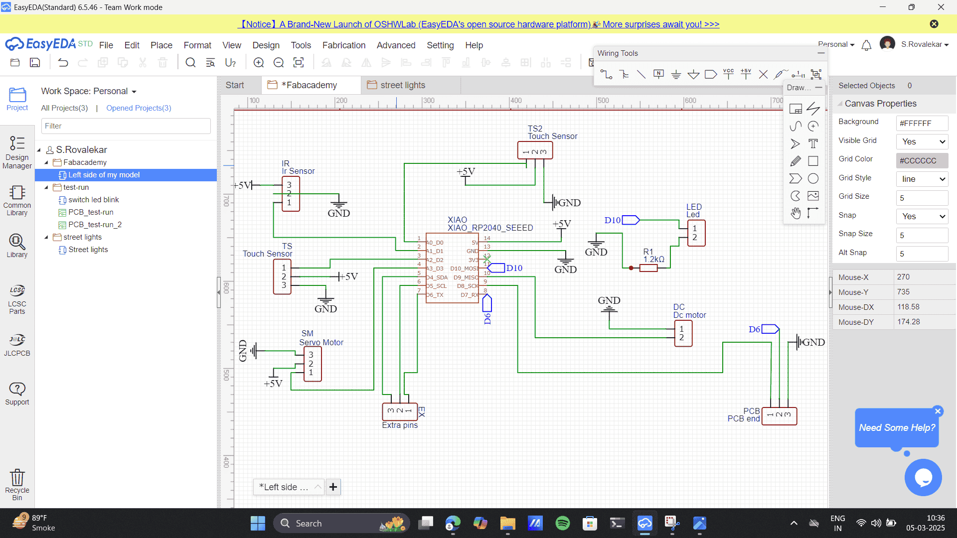
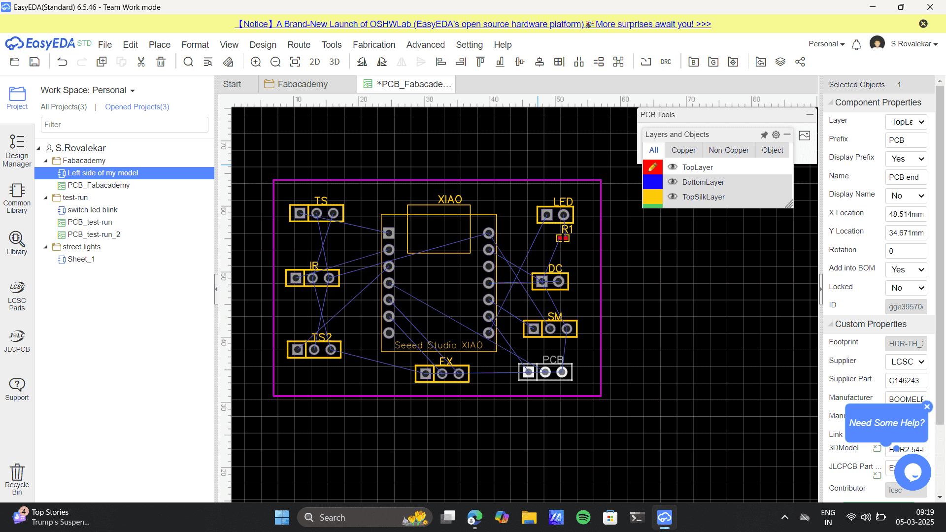
Final placements
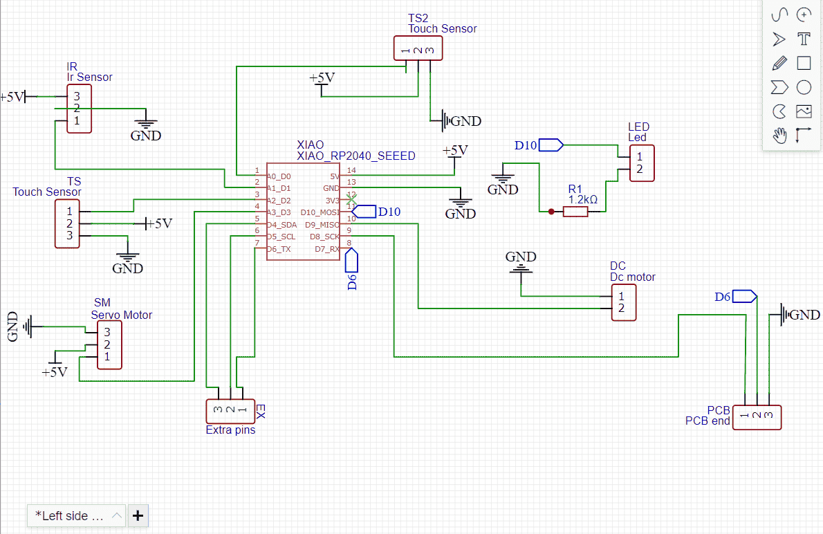
Using reference of schematic to build the pcb schematic
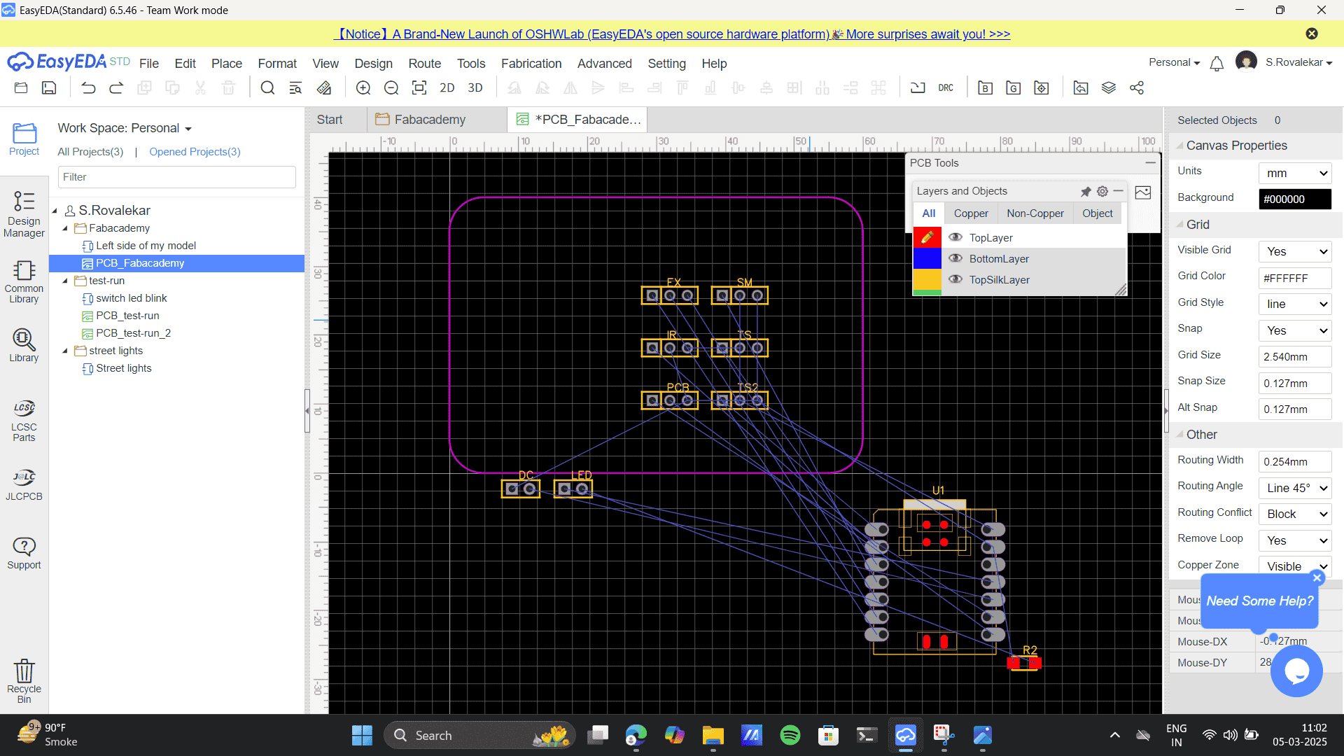
Placing components as per the schematic design
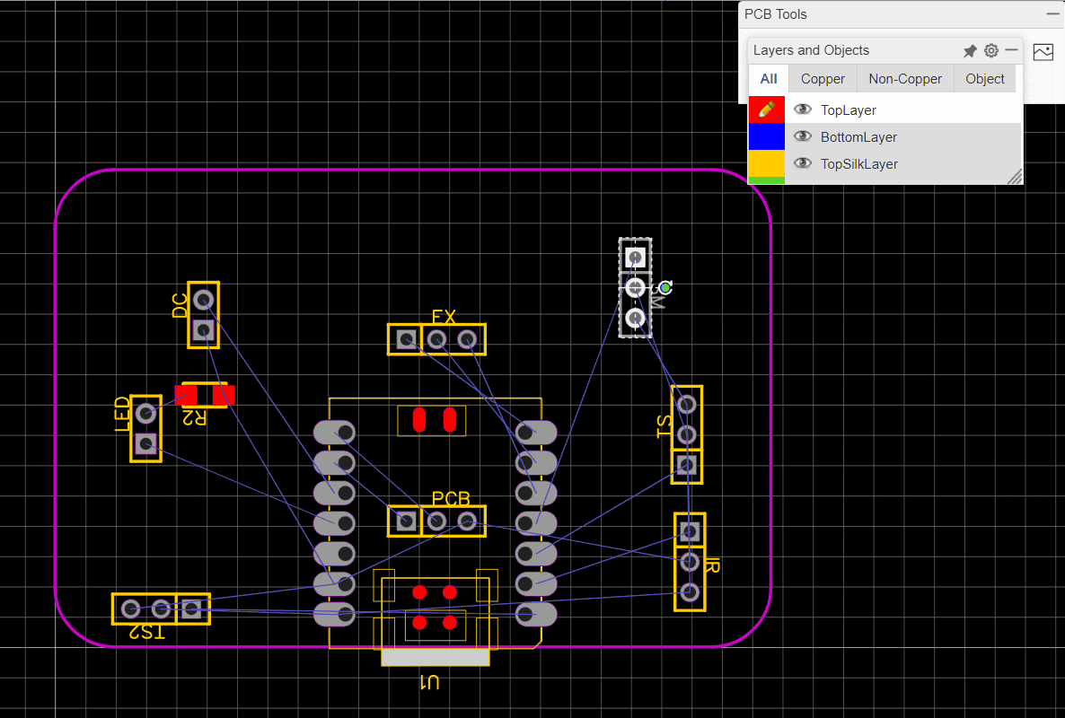
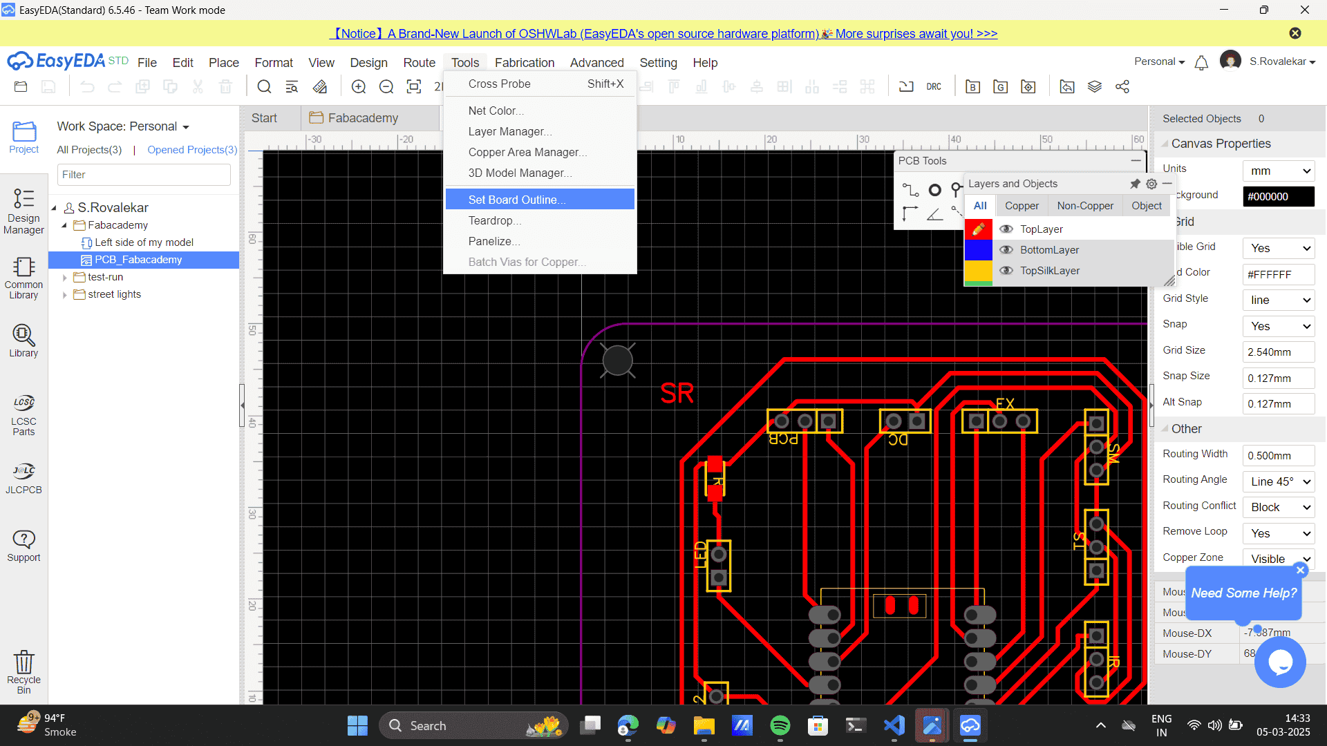
Auto route gave me yet another error. This time I went with a different approach. I realized that my board outline restricted the auto-route process and hence the DRC gave an error. Thus, I changed the board size by-
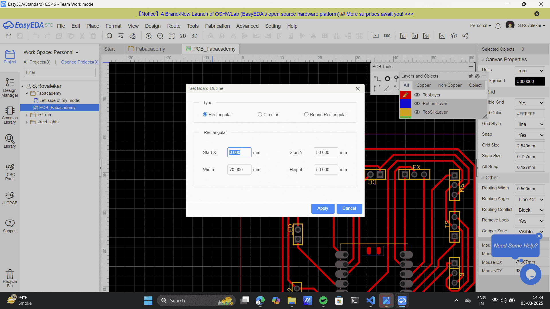
Changed the board size> Tools> Set board outline.
Change board size to 70*50mm, Start X and Y as 0 and rounded rectangle type.
Set the components and route.
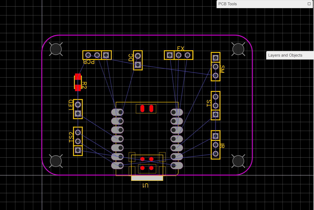
This gave me zero errors.
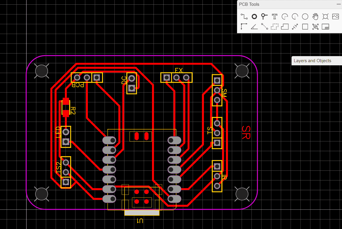
Fabrication> PCB fabrication file gerber file:
Hero Shots
2D
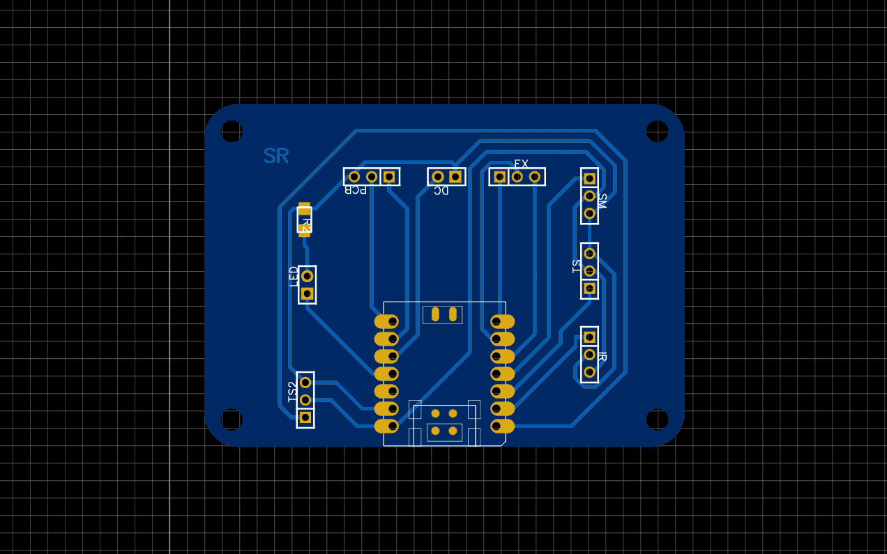
3D
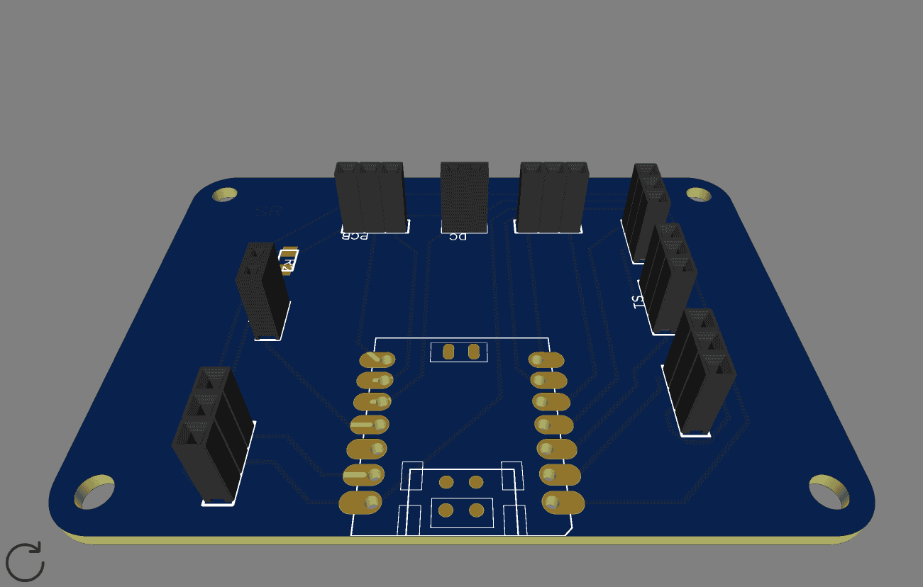
Fabrication> Generate gerber file.
Group Assignment
My friend Sharvari and myself worked together as a group to do this assignment. As part of the this , we used test equipment to analyze the operation of a microcontroller circuit board. The main tools we used were:
An oscilloscope is a tool used to visualize electrical signals in a circuit. It displays how voltage changes over time in the form of a graph, helping to analyze signal behavior, detect noise, and debug electronic circuits.
The Oscilloscope in Riidl Fablab is Tektronics tbs2000 seriers. This is the attatched data sheet..png)
Major part of this week's documentation is done by my friend Sharvari. Please refer to her documentation to dive deeper in our learnings of the oscilloscope: Sharvari Akerkar.
My learnings for group assignment: One of my biggest takeaways from working with the oscilloscope was getting comfortable with its grid and scaling system—once I figured that out, reading signals became much more intuitive. Seeing how it’s used in real-world applications, from troubleshooting circuits to testing components. For example, in audio equipment testing, an oscilloscope helps visualize sound wave distortions, ensuring high-quality output. What really stood out, though, was learning that an oscilloscope can be used to check the precision of another oscilloscope—a kind of self-check that reinforced how crucial accuracy is in electronics. Through this, I gained a solid understanding of the basics of oscilloscope.
Learning:The overall week was very heavy learning for me, from recalling curcuit diagrams from school to Designing a PCB was a huge brigde that I crossed. At the start the process seemed easy however, the actual usage of software with realtime connectivity needed higher level of attention. Performing the final project PCB design also helped me got a clearer idea of the process that I would utlilize to build the whole structure. Overall the whole week was a beautiful learning experince with many errors (especially getting the right Xiao from the library) and so much learnings.
Project files
Gerber fileGerber file 2
Image Link
Ribbon connectorsDiode and transistors
Mosfet