06. Electronics Design
Summary
This week I designed my first PCB using the KiCAD EDA software. For this week's group assignment, we had to characterize the design rules for our in-house PCB production process and submit a PCB design to a board house.
1. Basics of Electronic Design and PCBs
Electronic design involves the creation of circuits that allow electrical signals to perform specific functions. This process includes selecting components, designing schematics, and laying out circuits on a PCB.
A Printed Circuit Board or PCB is a physical platform that connects electronic components using conductive tracks etched onto a non-conductive substrate. PCBs provide mechanical support and reliable electrical pathways for various electronic applications, and their use has become a staple of modern electronics.
A PCB has the following key elements:
- Substrate - The base material, commonly a glass-reinforced epoxy laminate material known as FR4, which provides mechanical structure.
- Copper Layers - Conductive pathways that interconnect components.
- Solder Mask - Protective coating that prevents unintended electrical connections.
- Silkscreen - Labels and markings for component placement.
2. EDA Software
Electronic Design Automation software is a category of tools used for designing electronic circuits, including schematics, PCB layouts, and simulations. These tools help us through the design process by providing an environment to create, analyze, and test circuits before fabrication.
Some of the most widely used EDAs are:
- KiCAD - Open source PCB design tool with schematic and layout capabilities.
- Eagle - Autodesk's widely used tool with an extensive component library and Fusion 360 integration.
- Altium Designer - Professional grade software known for its advanced features and high quality PCB routing.
- EasyEDA - Web based tool suitable for beginners and online collaboration.
- OrCAD - Industry level software with advanced simulation and design features.
3. KiCAD
KiCAD is a free and open source EDA software used for schematic capture and PCB layout design. It provides an integrated workflow for designing electronic circuits and preparing them for fabrication.
KiCAD is widely used due to its flexibility, strong community support, and compatibility with professional workflows. It supports multi layer designs, differential pair routing, and 3D visualization, making it a great tool for both beginners and advanced users.
Here are its most notable characteristics:
- Open source - Free to use with active community support and frequent updates.
- Eeschema - A schematic editor for creating circuit diagrams and defining electrical connections.
- PCBnew - A PCB layout editor for designing board layouts.
- Component Library - Extensive libraries with predefined symbols and footprints for components.
- Design Rule Check (DRC) and Electrical Rules Check (ERC) - Tools to validate schematics and PCB layouts to ensure correct electrical connections.
- Gerber Export - Ability to generate manufacturing files required for PCB fabrication.
- 3D Viewer - Integrated tool for visualizing the PCB design in 3D.
4. KiCAD Eeschema
I began my design with the schematic editor, here are the steps that I followed:
4.1 Open Program and Install New Libraries
 Before getting started with my designs, I installed the libraries that were provided to us by our instructor.
After starting the program, I select the preferences option at the top of the screen and then the manage symbol libraries option. I scroll to the bottom of the chart and click on the plus sign near the bottom left corner. I set the nickname as "fab" and click on the folder sign on the right of the library path cell, I then select the KICAD_SYM file that was provided to us and select OK.
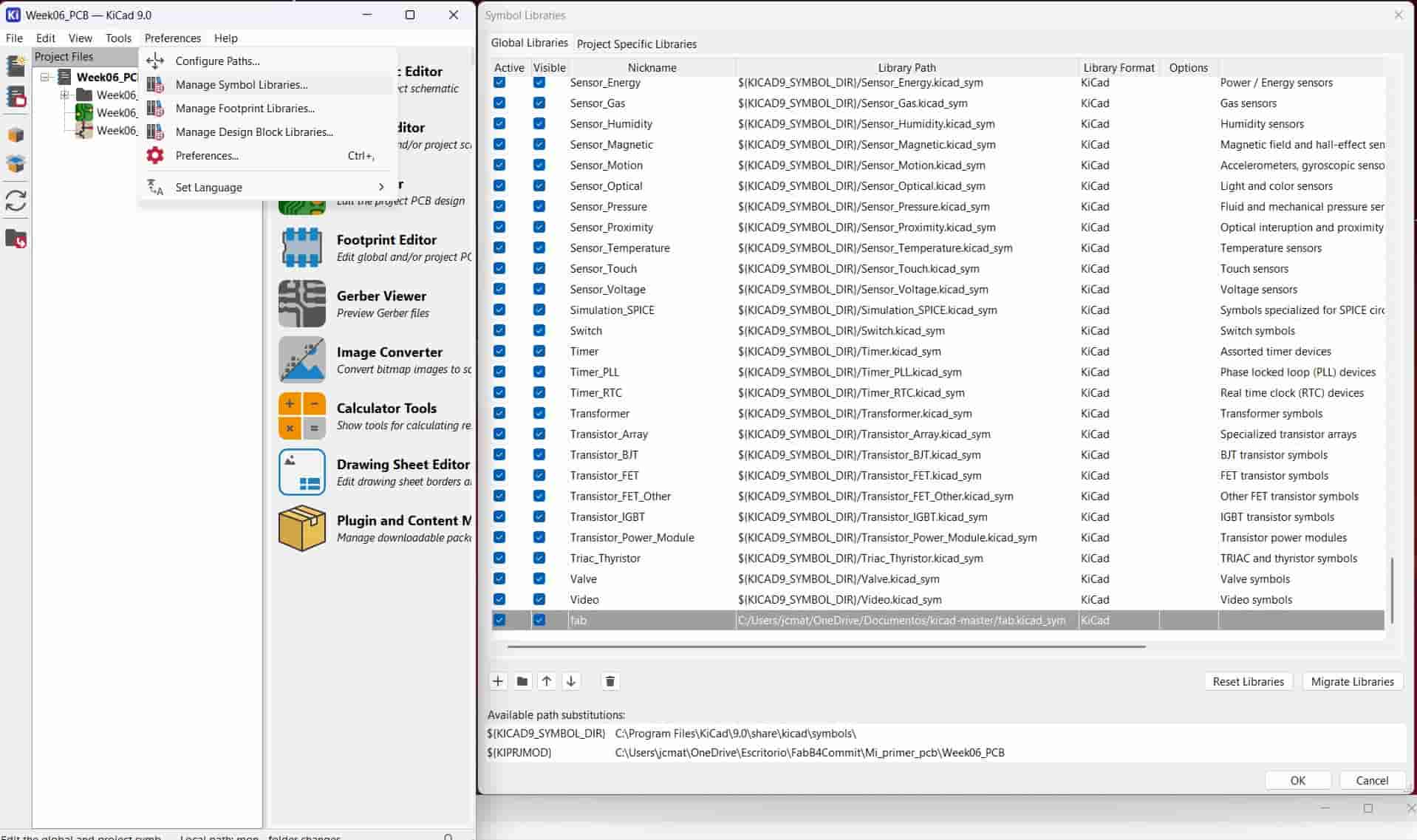
I repeat this process with the footprint library, selecting the "fab.pretty" folder instead.
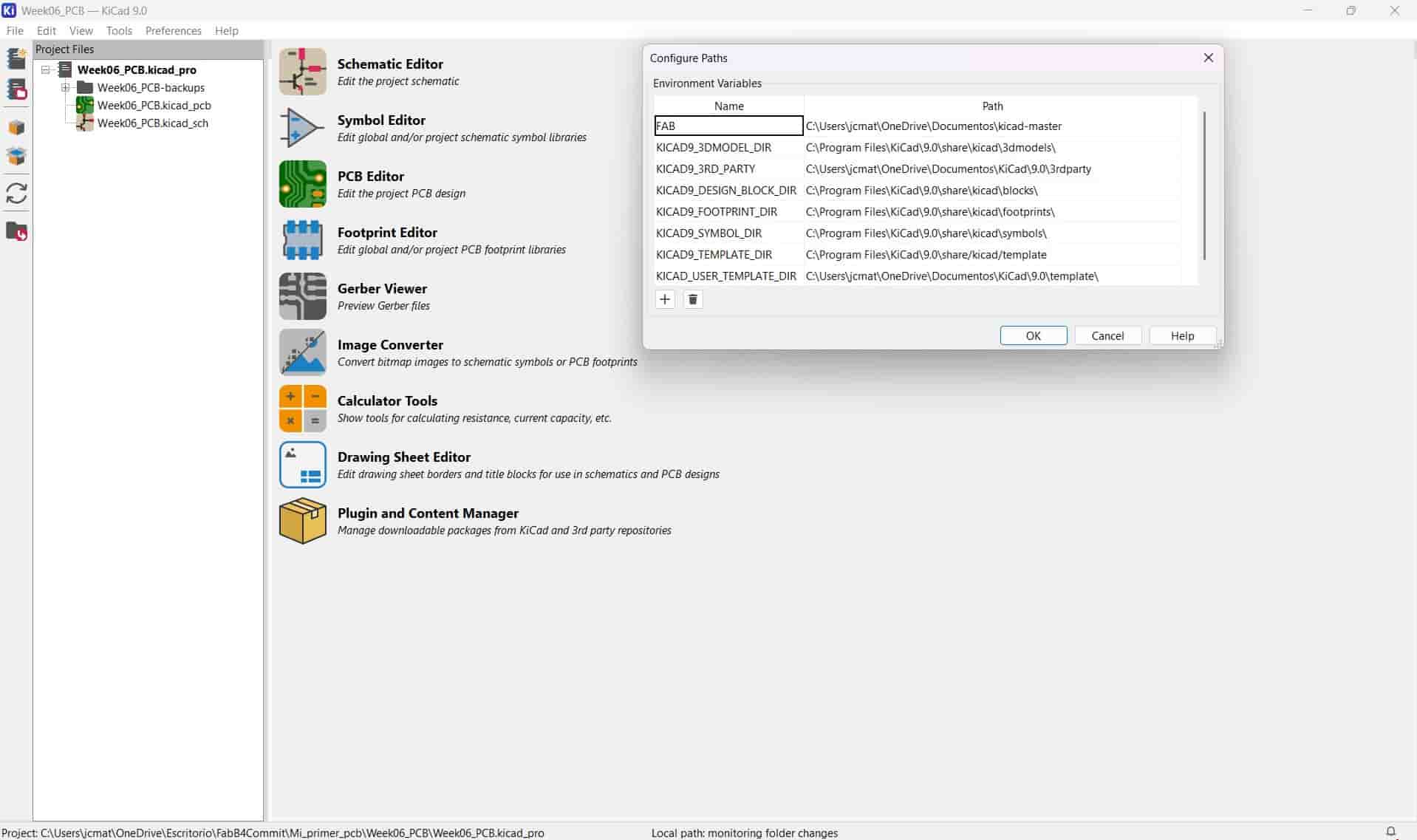
Finally, I configure a path to the "kicad-master" folder. With this we are set to begin with our designs.
4.2 New project & Eeschema
We create a new project and open the eeschema or schematic editor, here is where we will develop the schematic for our PCB.
In the schematic editor, we will place our components and draw the connections between them.
The tools on top of the UI are used mainly for visualization purposes, while the tools on the right are used to insert elements into the schematic.
4.3 Place Component Symbols
On the right side of the screen we will see a right facing triangle with a - and + inside. We will click on it and the symbol menu will open.
In the symbol menu we can find all of the different components from our libraries, each with a corresponding footprint. If needed, we can install more libraries as explained in the first step.

We begin by placing the XIAO-RP2040, which will be the centerpiece of our circuit.
4.4 Place Power Symbols
We will be using many power symbols in our schematic, so this is what we will place next. Right below the place symbols button, we can see a ground symbol, when we click on it, the power symbol menu will open.
From this menu we can insert different power symbols, for this PCB, we want the PWR_3V3 symbol, the PWR_5V symbol and the PWR_GND symbol.
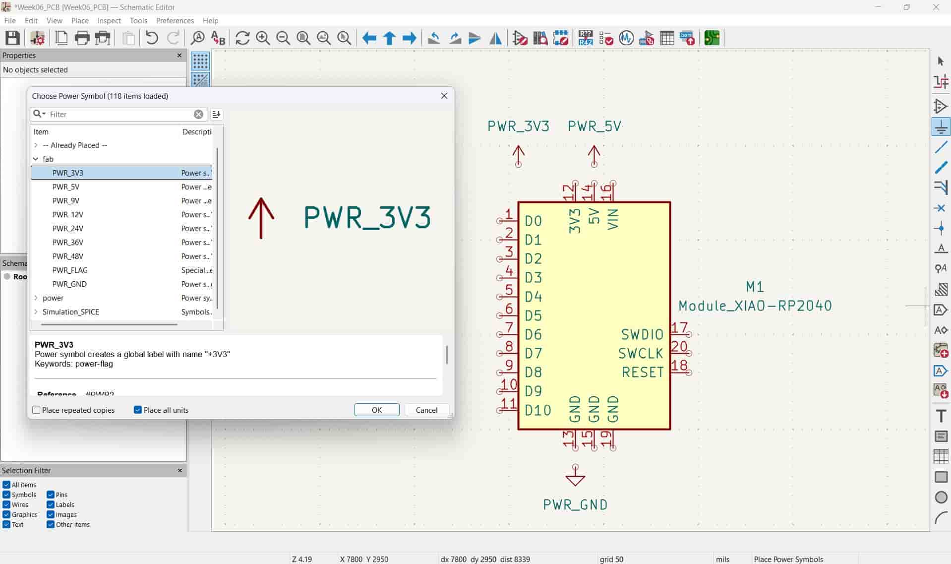
Its important to note that the XIAO's inputs should be 3V3, since that is the voltage that the XIAO operates at 3.3V logic.
4.5 Wiring
Below the place power symbols button is the draw wires symbol, denoted by a diagonal line. We will click on it and then click on any of our component's terminals, from there we will drag the wire to another component's terminal, establishing a connection between both components.
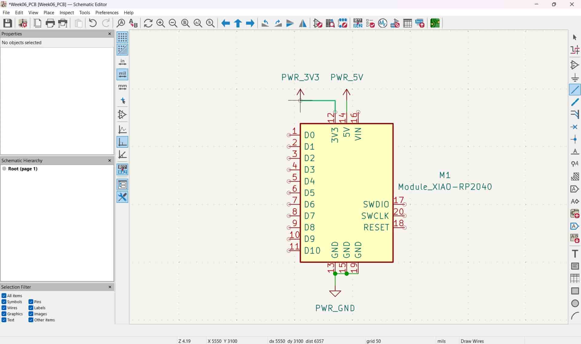
We can also place a component directly on top of another component's terminals, which will automatically connect them with a wire.
4.6 Labels
Right in the middle of our tools we will see a black polygon with an A in it, this is the place global labels button.
Global labels are very useful to maintain a tidy schematic, when we place a label, it will be synchronized with every other label of the same name.
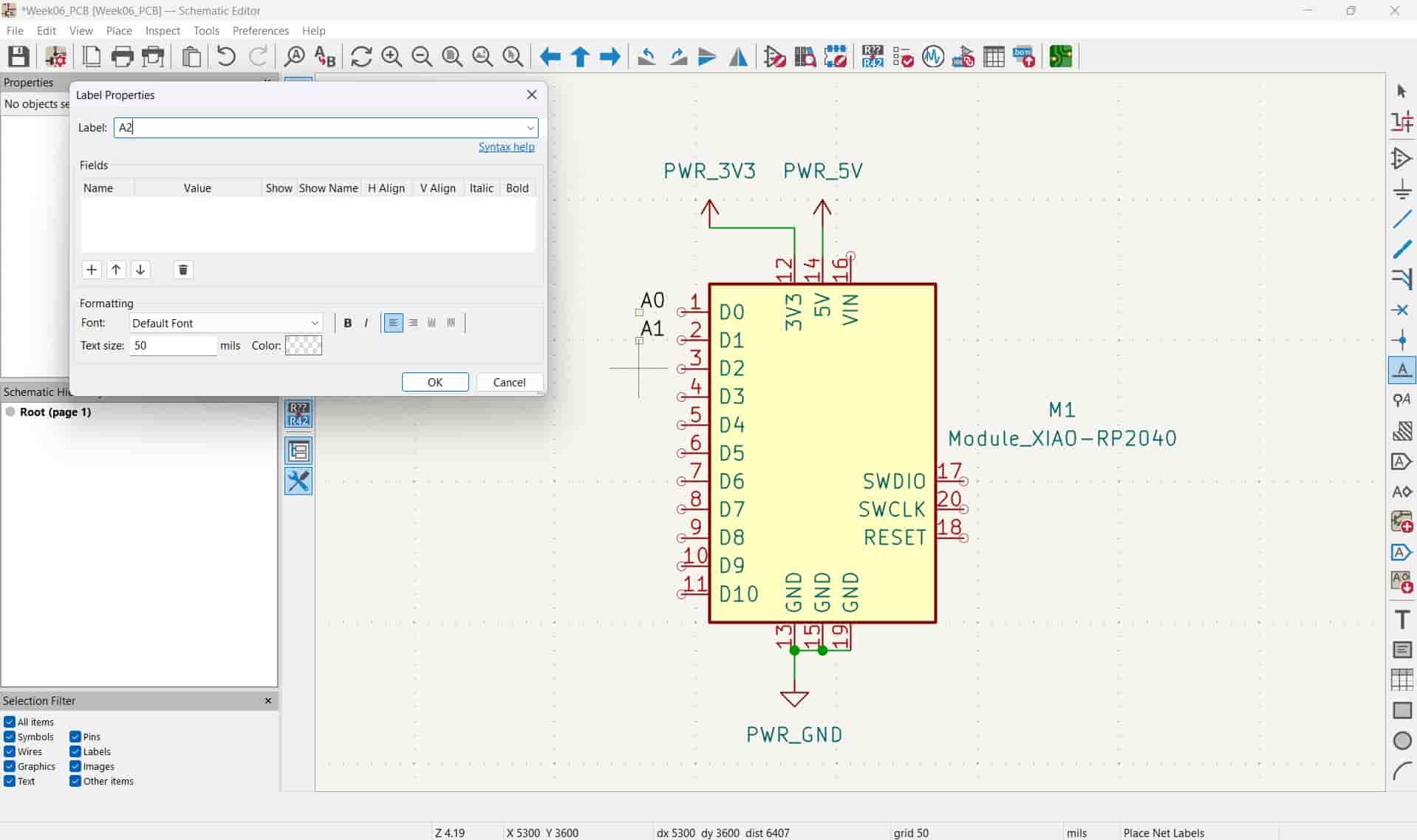
I applied labels to all of the I/O pins on the XIAO, which will allow me to draw different parts of the schematic without having wires all over the screen.
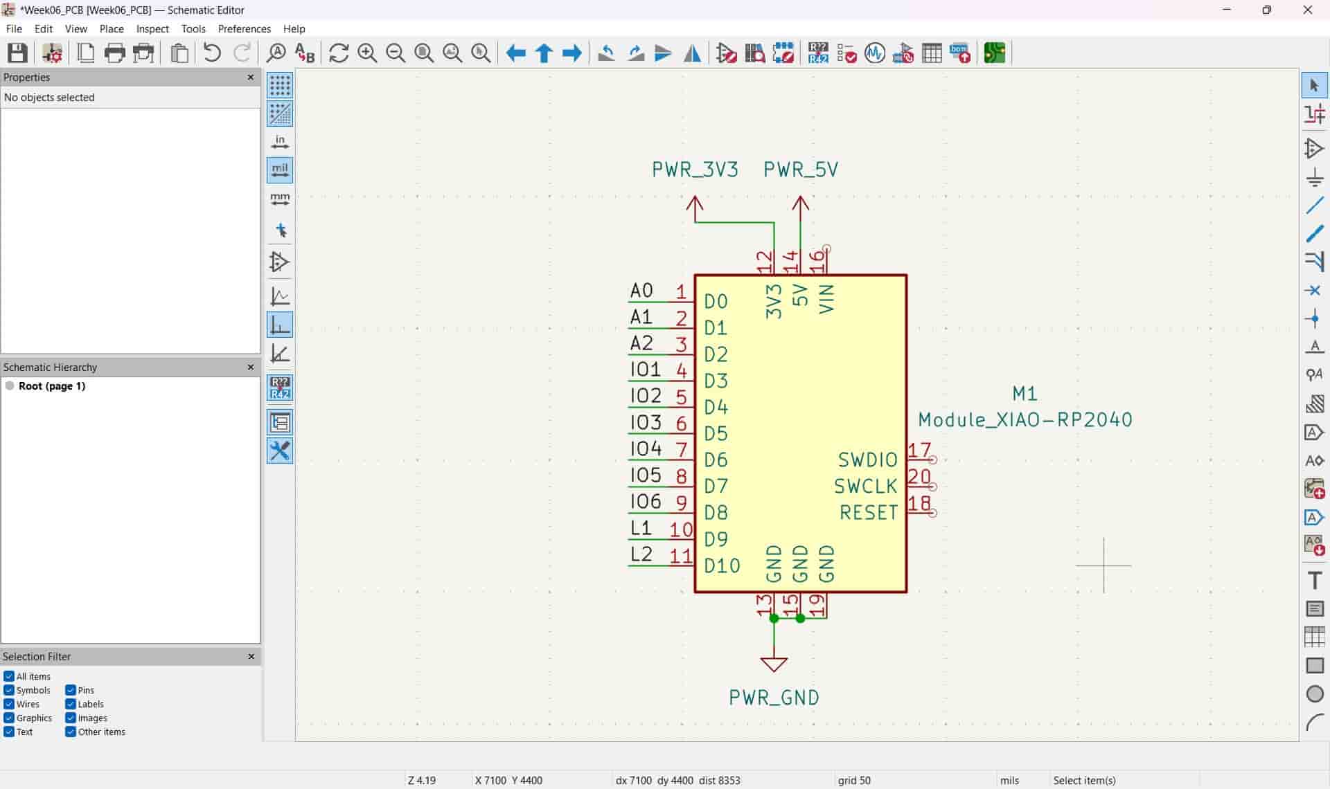
4.7 Input Pins
The fist elements that I will add to my XIAO are a pin socket for analog inputs and a pin header for digital inputs.
I place these components from the component menu and add the corresponding labels.
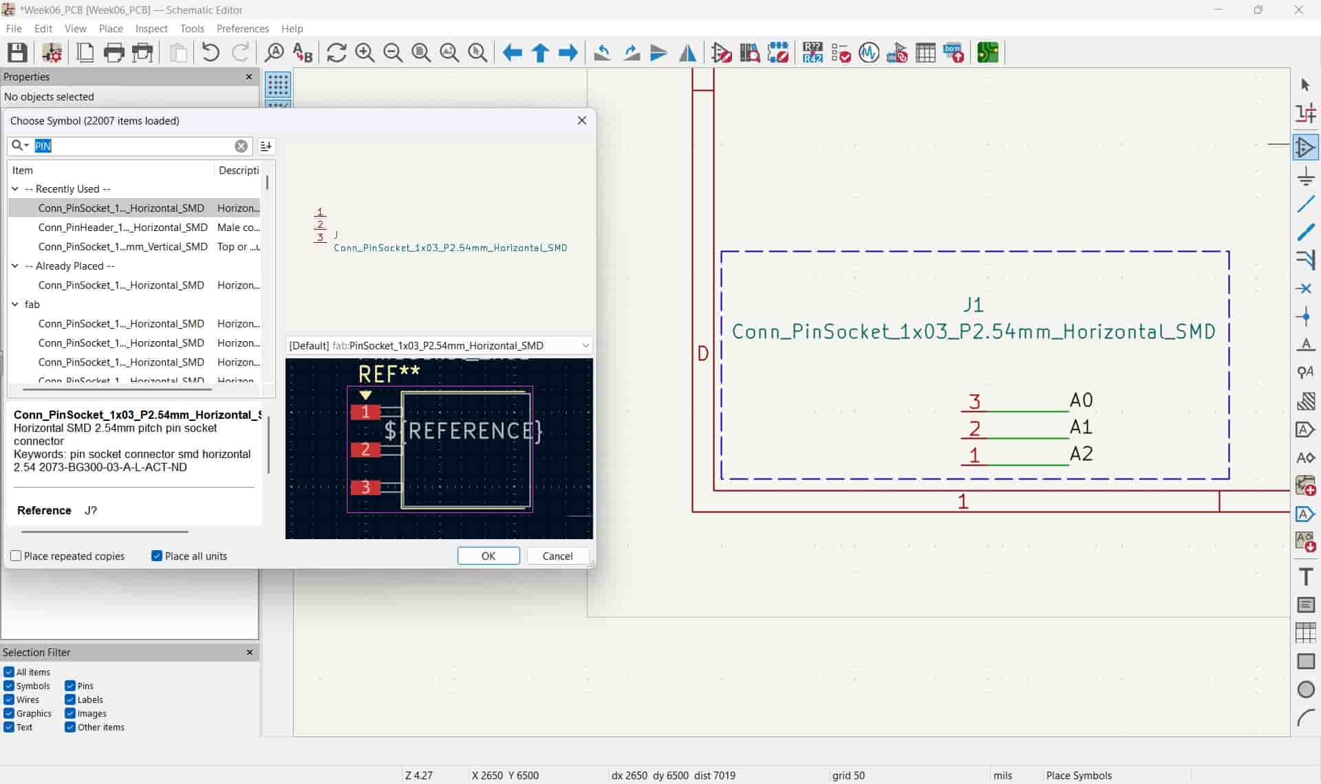
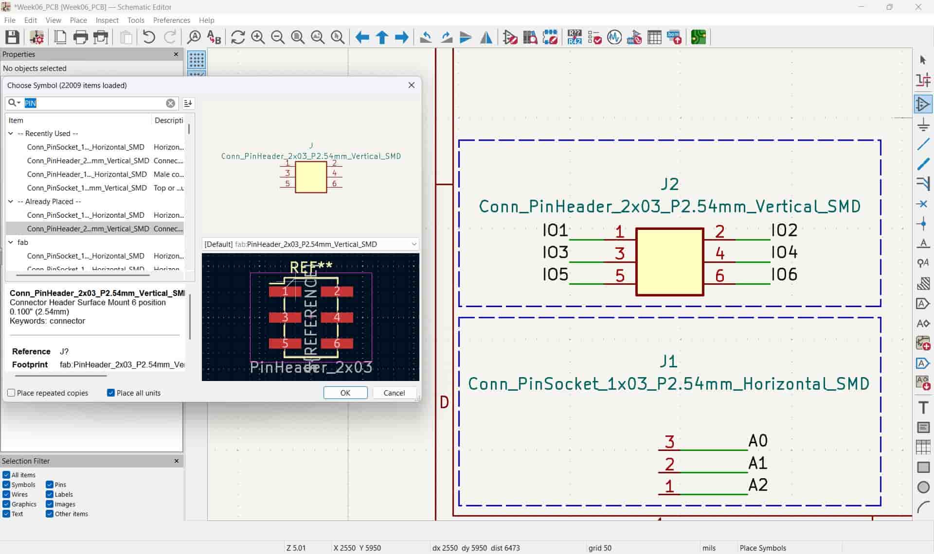
Its important to note that the XIAO only has three specific pins that can receive analog inputs, which you can find in the XIAO's pin layout.
4.8 Text and Rectangles
The five tools at the bottom right of the screen are used to add annotations that won't have an effect on the schematic, but are useful for identification and organization.
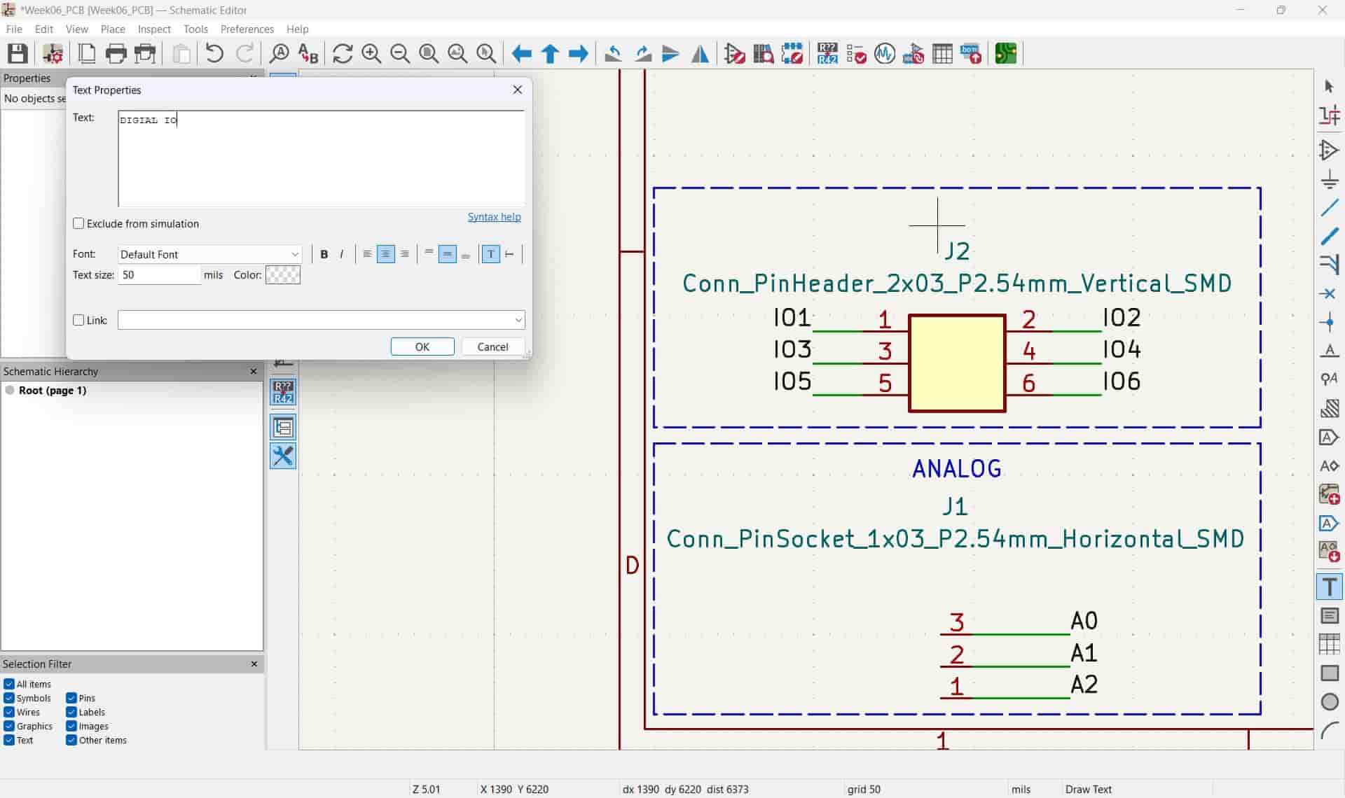
I use the rectangle tool to divide each specific subsystem based on its function and use the text tool to state said function, you can also edit the properties of these elements through the menu on the left side of the screen.
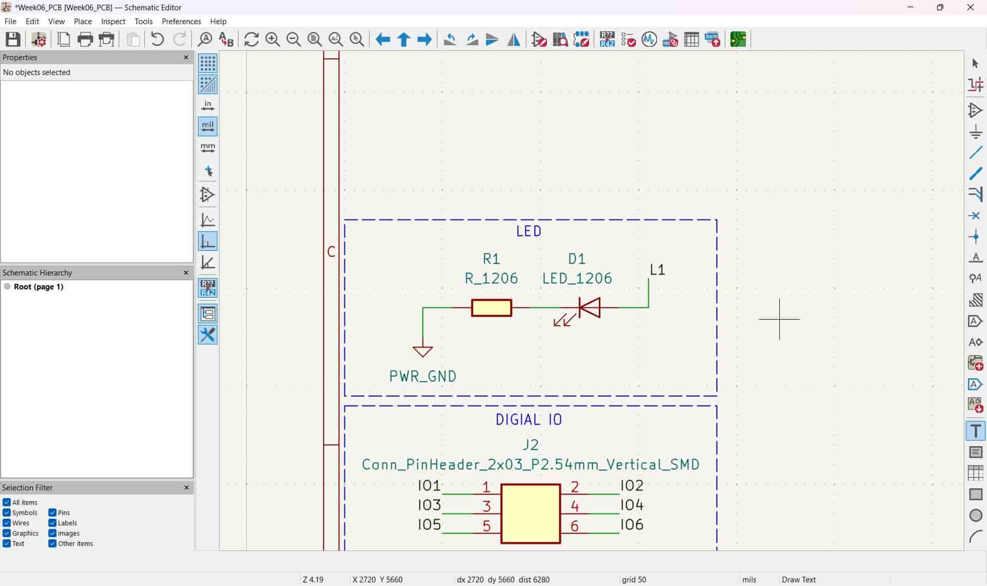
4.9 LED
To create a funcional LED subsystem we need to insert two components, an LED and a resistor, but we won't be working with the usual through-hole components, we will instead be working with surface-mount components, which are soldered directly on top of the PCB.
Surface-mount components come in a variety of sizes, but share the same funcionality. To maintain a balance between compactness and easy handling, we will be working with 1206 components, which are 3.20 x 1.60 mm.
We open the place component menu and insert a 1206 LED and a 1206 resistor, we then wire them to the label corresponding to the pin on the XIAO and to ground.
The value that I chose for the resistor which after the LED was 1kΩ, this will limit the current to 1.3mA, which will keep the LED visible and maintainin power efficiency, while preventing the LED from burning from an excess of current.
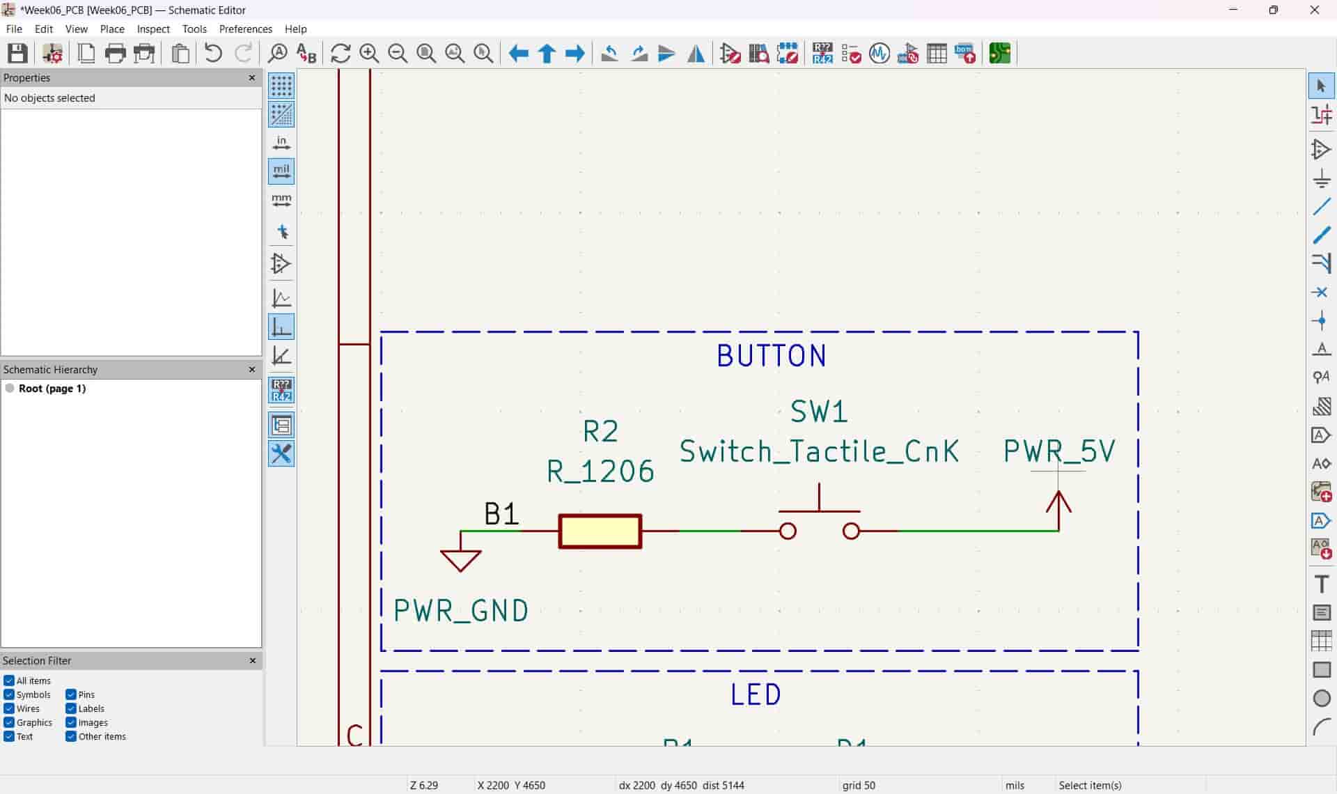
4.10 Button
We will make a button in a pull-down configuration, which means that the default state of the input will be false. We insert the button, the resistor, the label, power and ground.
We wire the power to the button and place the label on the other side, we then continue to the resistor and end at ground.
The vaule that I chose for the pull-down reistor was 10kΩ, which is a standard value used in digital electronics because it pulls the pin LOW reliably without wasting power, ensuring stable, low power operation when the button is not pressed..
4.11 Voltage Regulator
The final subsystem of our PCB is the voltage regulator, which will recieve electrical signals and turn them into 3.3V signals. I had no previous knowledge about these regulator systems prior to their introduction by our instructor, but to find how we can find out how to integrate them into our PCB, we can look for the datasheet of the component, and copy the intended applications.
From the intended applications, we can copy the components and wiring that the system requires, which is precisely what we did to integrate the system into our schematic.
The regulators output voltage is 3.3V, which is the voltage that the XIAO uses to operate, the value of the capacitors is of 10µF on the input side and 22µF on the output side. The input capacitor reduces voltage ripples from the power source and helps smooth sudden changes in current draw. The output capacitor keeps the 3.3V line stable when the circuit's current demand changes and prevents oscillations in the voltage regulator. The 10µF and 22µF values are recommended in most regulator datasheets, since larger caps handle power fluctuations better than smaller ones such as lµF, but too much capacitance can slow down response time, so 10µF and 22µF are a good balance.

4.12 Electrical Rules Checker
Once we are finished with the schematic, we have to use the Electrical Rules Checker or ERC to check for any errors in our design.
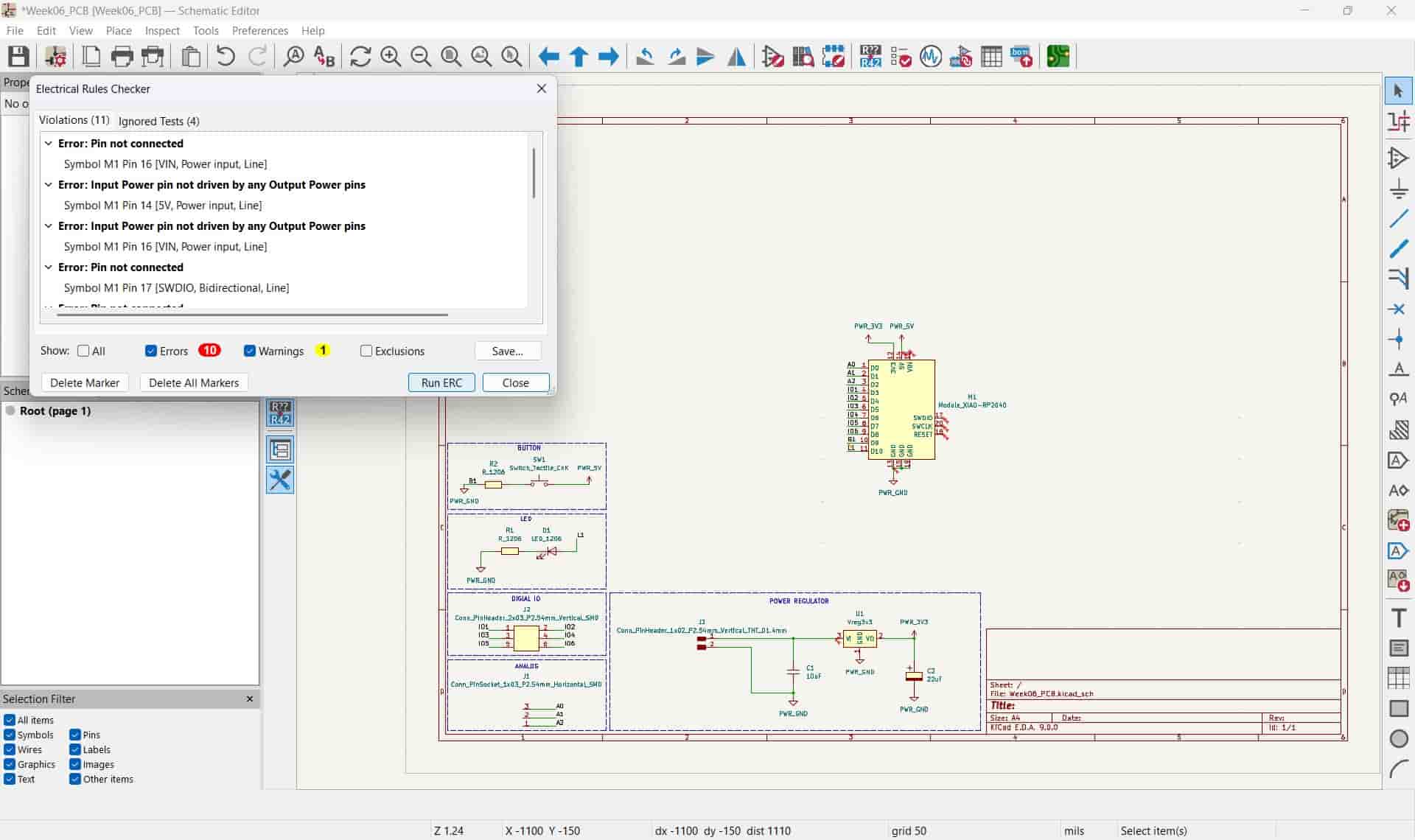
We open the inspect menu and select the Electrical Rules Checker, we then run the ERC, which will display all possible errors in our schematic.

It's worth noting that any unused pins will be classified as an error, to bypass this we will use the place no connect flags tools, denoted by a line and a cross. We will place one of these crosses on any unused pins. When we run the ERC again, these errors will disappear.

Some other errors will persist, but they won't have any effect in our current purposes.
If we are satisfied with the results provided by the ERC, we are finished with the schematic.
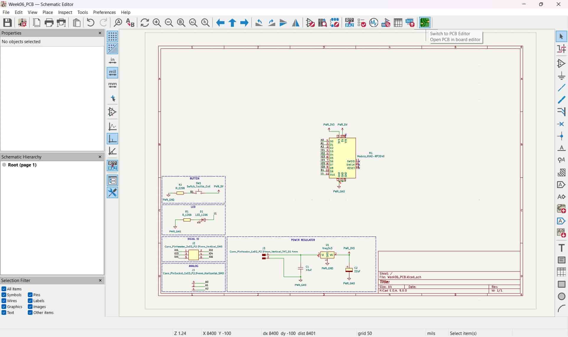
5. KiCAD PCBnew
From the schematic editor, we can go to the PCB layout editor, we do this by clicking on the icon with the image of a PCB on the top of the screen.
5.1 PCBNew
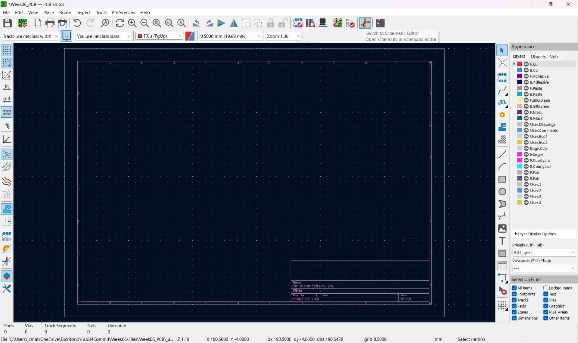 Once we are in the PCB layout editor, we have to update the PCB from the schematic. We do this by clicking on the icon with half a schematic and half a PCB on the top of the screen and then on the update PCB button, this will import all of the components present on the schematic.
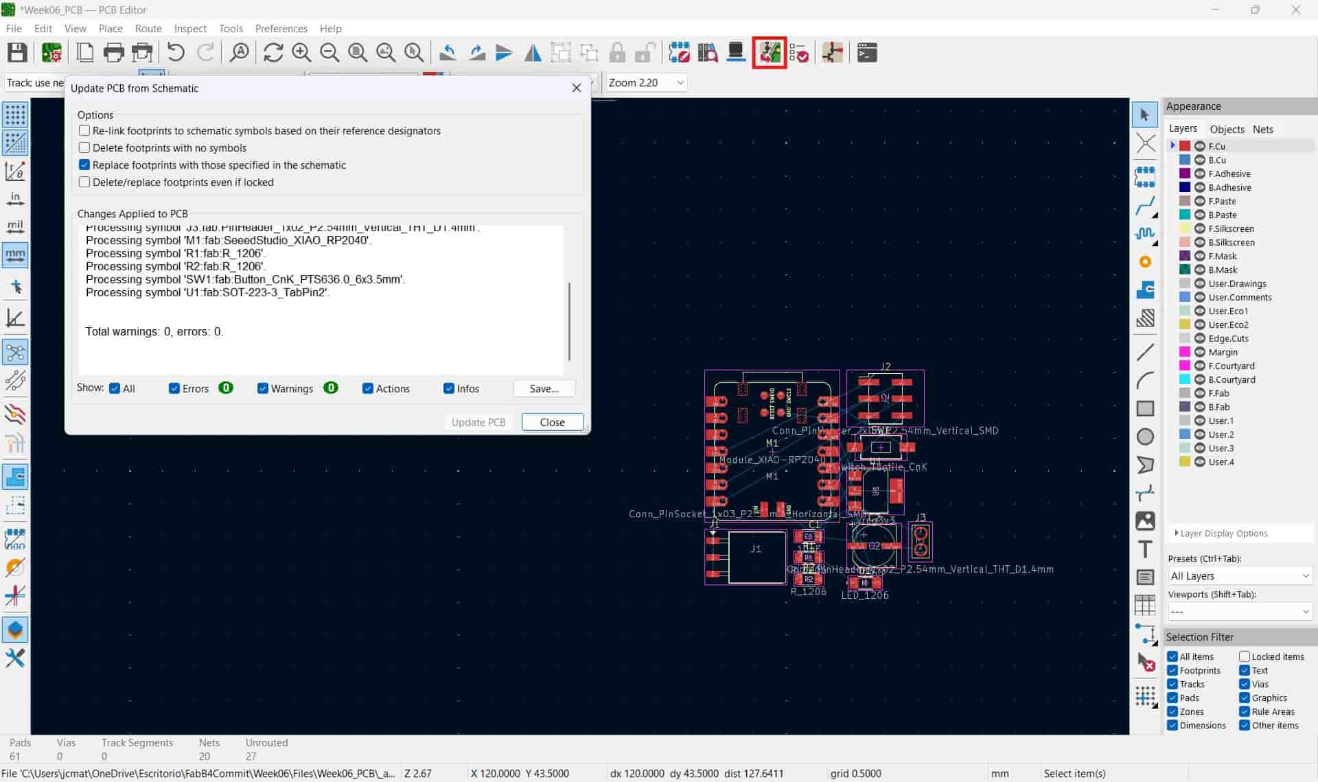
Now, as you may notice, the PCB suddenly looks very cramped, so we will hide all of the layers that aren't relevant to our purposes, leaving visible the Front Copper, Front Silkscreen and Front Mask layers.
We can move a group of components or individual components around the screen, which will arrange in accordance with the design's intended connections.

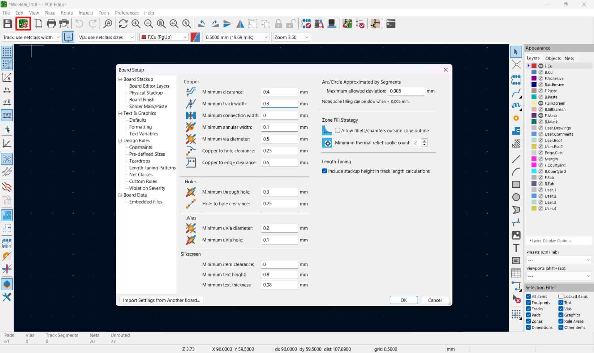
5.2 Calculations
Before we begin routing, we have to determine the width of our routes and the spacing between them, we will do this by using the calculator tool.
To access the calculator, we go to the KiCAD's main menu and select the calculator icon, this will open the calculator tools program.
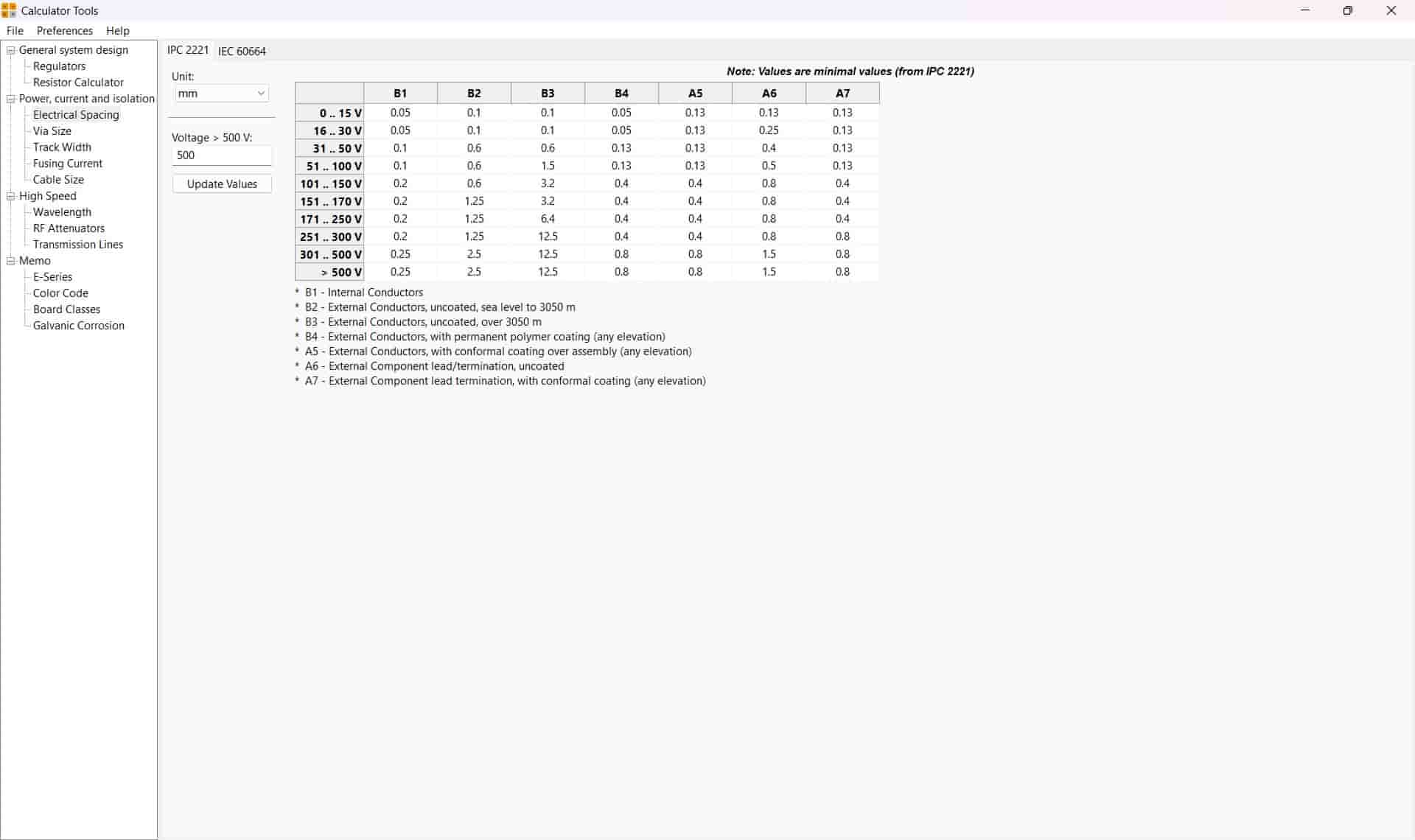
Once in the calculator, we can consult the electrical spacing chart to determine the minimum distance required between our routes, in my case I will be working with B2 type conductors at no more that 12V, so the minimum electrical spacing is of 0.1 mm, however, I will be using 0.4 mm spacing to ease the soldering process.
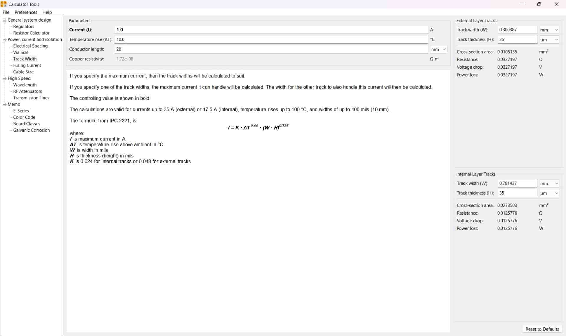
I then calculate the track width, where I input the maximum current and temperature rise parameters, which tells me that the minimum width is of 0.3 mm, I will go with 0.4 just in case. This calculation is important because having insufficient route width could lead to overheating or signal integrity issues.
Once we have calculated these parameters we can input them in the constraints section of the board setup menu, which we can access by clicking the icon with a PCB and a gear on the top left of the screen.
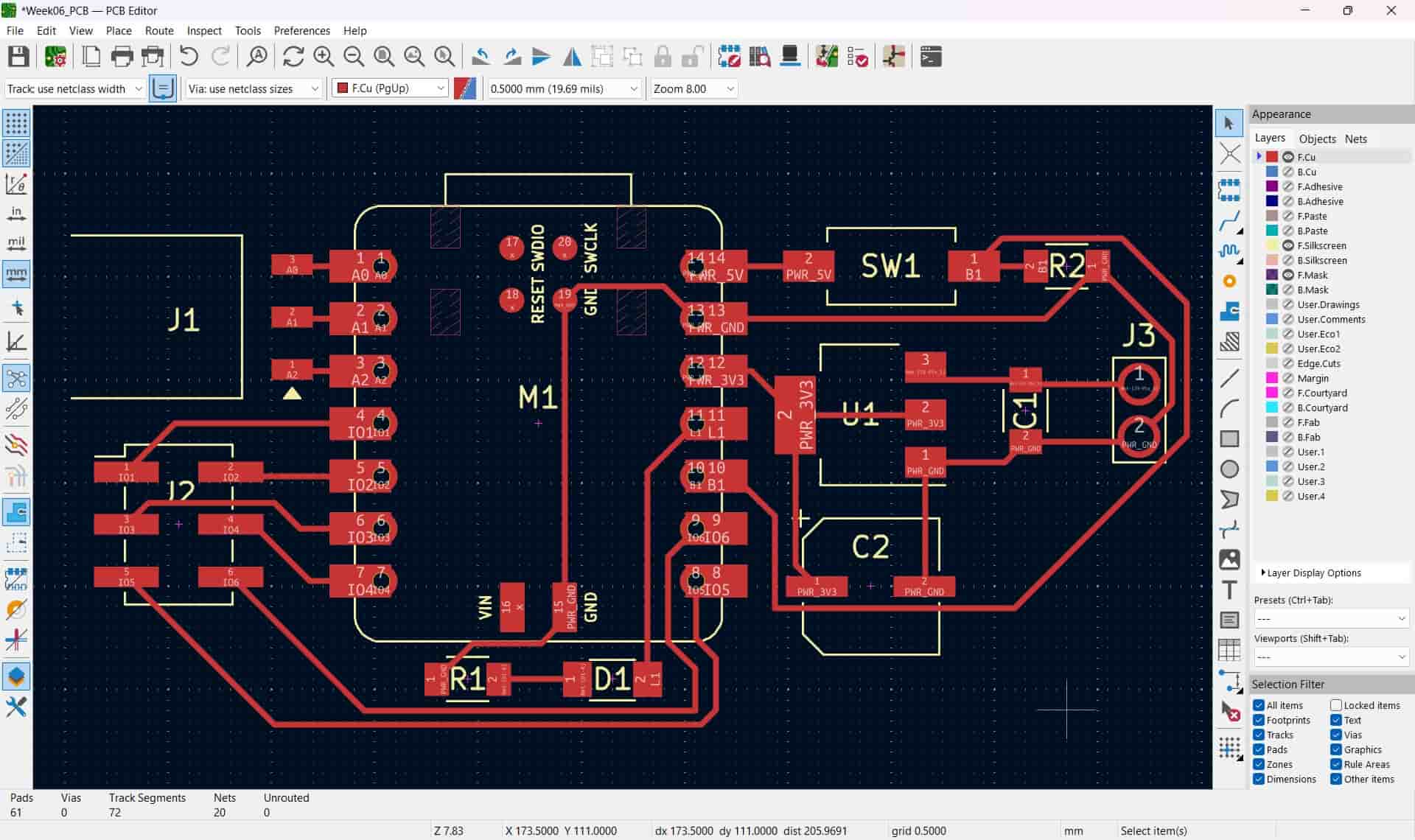
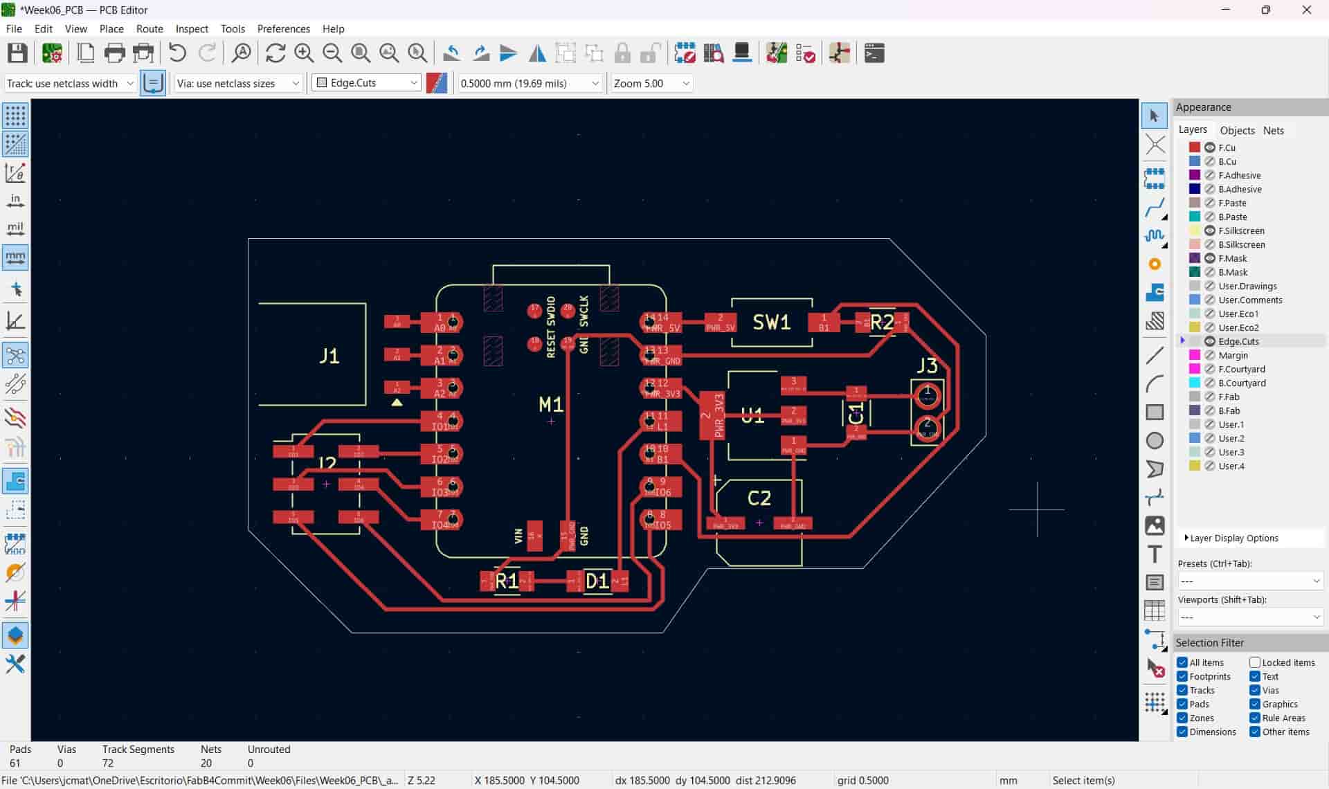
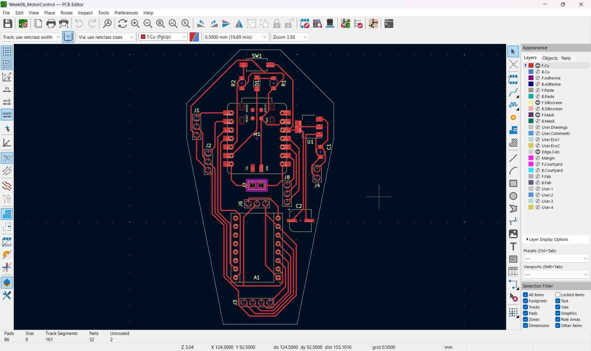
5.3 Routing
Now we can begin routing our components, this will establish the conductive routes of our circuit.
On the right side of the screen we can see an icon of diagonal blue line, this is the route single track icon. Once we press it, we can select any terminal of our components, and a route will be generated.
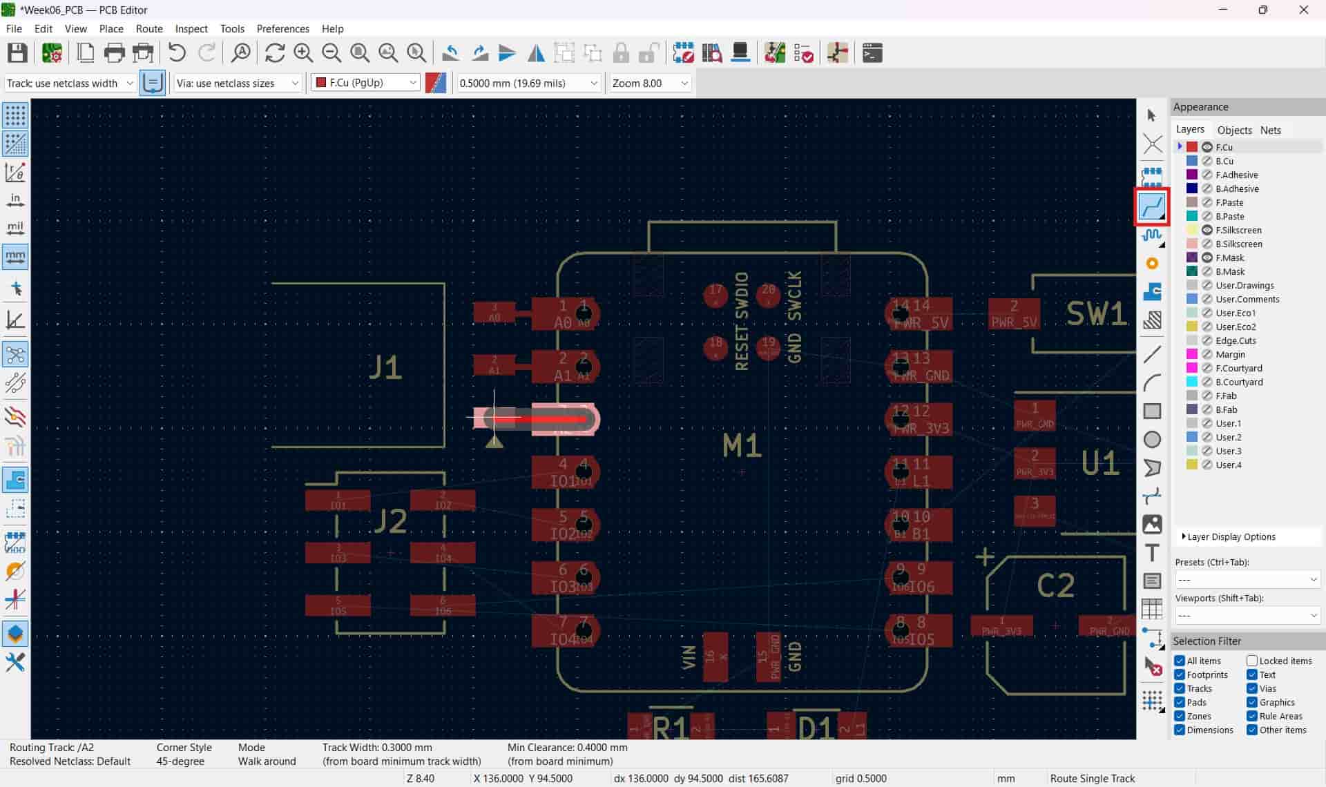
From there, we can drag the route around the circuit to our liking, connecting it to its intended destination.
We then route all of the components, which can be quite entertaining, since you have to establish the routes without touching other routes, except for the power and ground routes, it feels like solving a fun puzzle.
5.4 Drawing Edges
Once we have routed all of the components, we can draw the external edges of the PCB, which will determine the board's geometry and maximum dimentions.
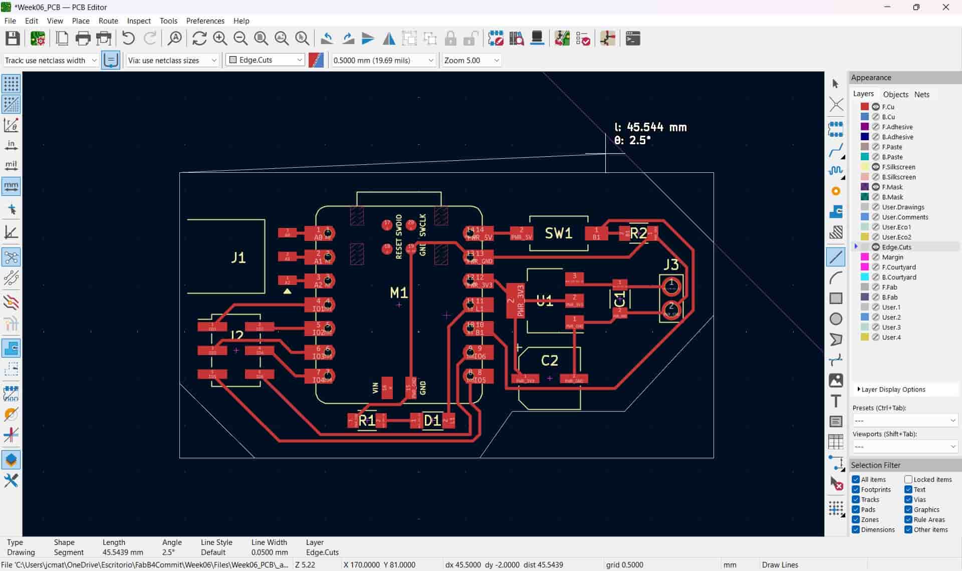
To do this we can use the grey tools at the right of the screen, such as the line tool, curve tool or rectangle tool.
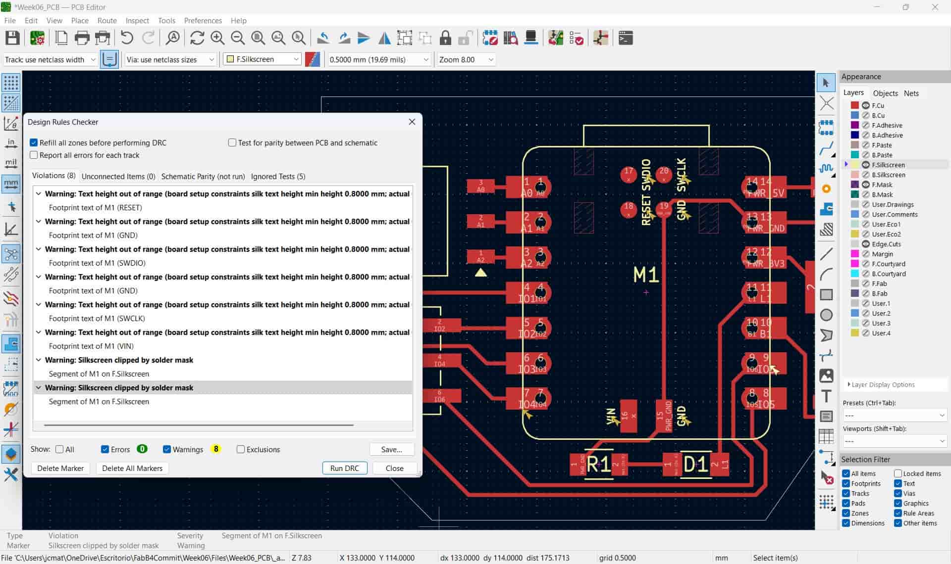
5.5 Design Rules Checker
Similar to the ERC, the DRC helps us analyze our design and identify potential flaws. To access the DRC, we open the inspect tab and select the Design Rules Checker, we then press run DRC.
My DRC generated various error messages related to text and the Silkscreen, which are irrelevant to me since I will only carve the routes, vias and edges during electronic production week.
Once we have rectified all the relevant errors, we have finished our design.
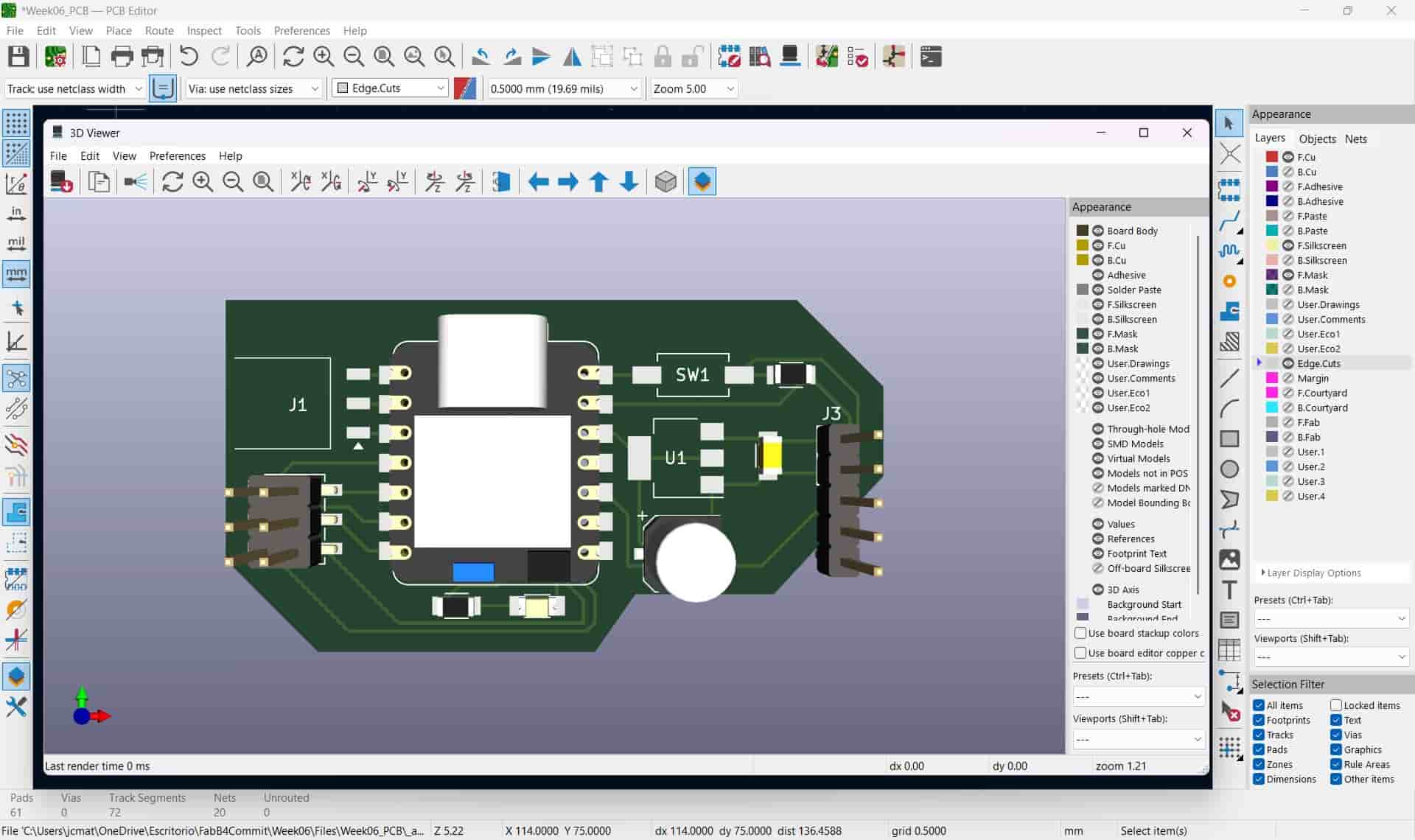
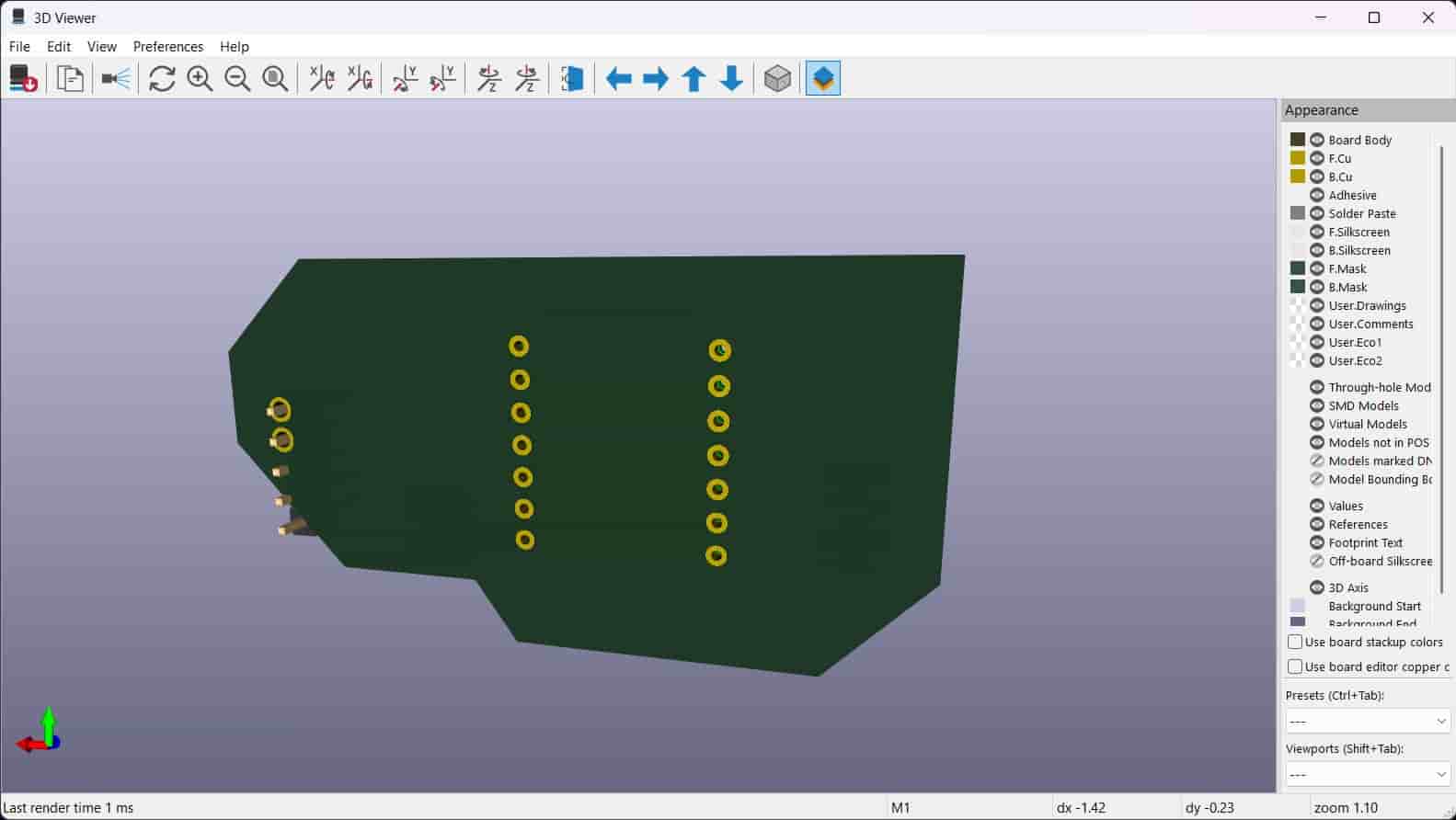
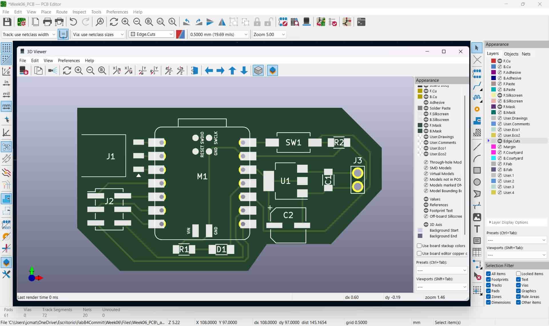
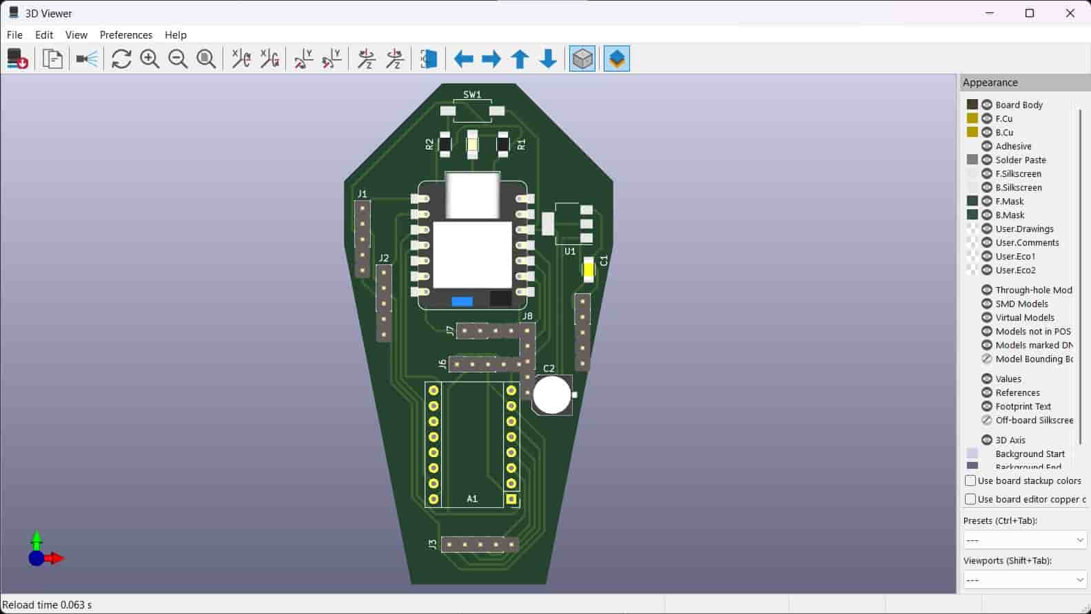
5.6 3D Viewer
We can generate a 3D model of our PCB with the 3D viewer, which will generate the PCB and the components that have a 3D model in our libraries.
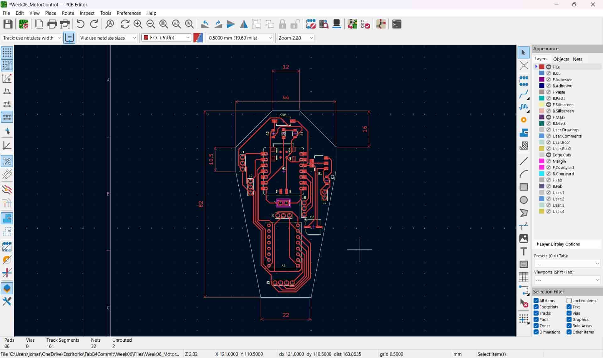
6. Motor Control PCB
I designed a second PCB intended for my final project.
The circuit consists of a XIAO-RP2040, an A4988 stepper motor driver, I/0 pins, a button and LED for debugging, a voltage regulator and a set of pins intended for two servomotors. This design was based on the simulated embedded system from week 4.
The resistors and capacitors are of the same values as the ones used in the first PCB.
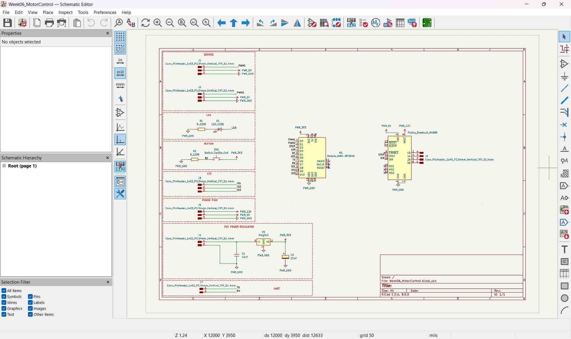
This system is supposed to take inputs from an OpenMV Cam H7, and process said inputs to engage our actuators.
It's worth noting that this design is still a work in progress, as I have still much to learn and integrate into the final version.
7. Case for Motor Control PCB
I decided to design a case for my Motor Control PCB, using SolidWorks.
First I took the measurements of the PCB's edges, and drew said edges on a sketch. I then proceeded to draw a larger outline to fit bores for M3 screws.
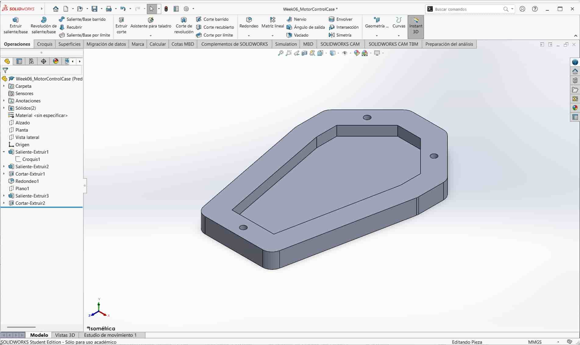
After extruding the base of the case, I generated an offset plane to draw the cover.

8. Comments and Recommendations
I recommend seeking insights on your circuits by an experienced colleage or your instructor, since we are new to electronic design, we could be ignoring important aspects of our design.
You can leave larger spacing between routes, use larger routes and leave more space between individual components to ease the electronic production process, though this will reduce the space efficiency of the design. Once you are more experience with the production process, you should try to optimize your designs as much as possible.
9. Learning Outcomes
This week I learned how to use EDA software and I designed two PCBs, with one being a general-purpose development board and the other being a motor controller for my final project.