11 - Embedded Networking and Communications
This week, we will learn how to establish communication between different embedded systems to exchange information in a secure and optimal manner. To do so, we will learn the most used communication protocols in embedded systems, as well as their advantages and disadvantages. To become familiar with different microcontrollers, we decided to use the ATtiny along with the XIAO RP2040, which has been used in previous weeks.
INTRODUCTION
Communication protocols are rules that allow the exchange of information between devices connected to a network. Their goal is to enable devices to communicate with each other efficiently, securely, and reliably. Below are some of the most popular communication protocols in embedded systems.
I2C
I2C communication only uses two wires to transmit information between devices.
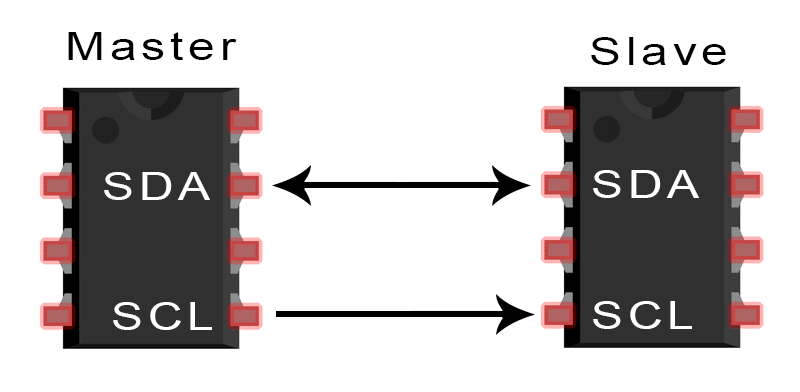
- SDA (Serial Data) - The line for the master and secondary to send and receive data.
- SCL (Serial Clock) - The line that carries the clock signal.
With I2C, data is transferred in messages. Messages are broken up into frames of data. Each message has an address frame that contains the binary address of the slave, and one or more data frames that contain the data being transmitted. The message also includes start and stop conditions, read/write bits, and ACK/NACK bits between each data frame:
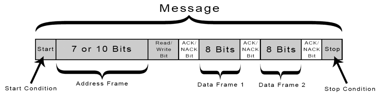
- Start Condition: The SDA line switches from a high voltage level to a low voltage level before the SCL line switches from high to low.
- Stop Condition: The SDA line switches from a low voltage level to a high voltage level after the SCL line switches from low to high.
- Address Frame: A 7 or 10 bit sequence unique to each slave that identifies the slave when the master wants to talk to it.
- Read/Write Bit: A single bit specifying whether the master is sending data to the slave (low voltage level) or requesting data from it (high voltage level).
- ACK/NACK Bit: Each frame in a message is followed by an acknowledge/no-acknowledge bit. If an address frame or data frame was successfully received, an ACK bit is returned to the sender from the receiving device.
SPI
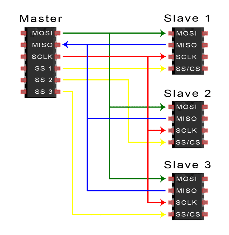
Devices communicating via SPI are in a master-secondary relationship. The master is the controlling device (usually a microcontroller), while the secondary (usually a sensor, display, or memory chip) takes instruction from the master. The simplest configuration of SPI is a single master, single secondary system, but one master can control more than one secondary.
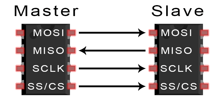
- MOSI (Master Output/Secondary Input): Line for the master to send data to the secondary.
- MISO (Master Input/Secondary Output): Line for the secondary to send data to the master.
- SCLK (Clock): Line for the clock signal.
- SS/CS (Secondary Select/Chip Select): Line for the master to select which secondary to send data to.
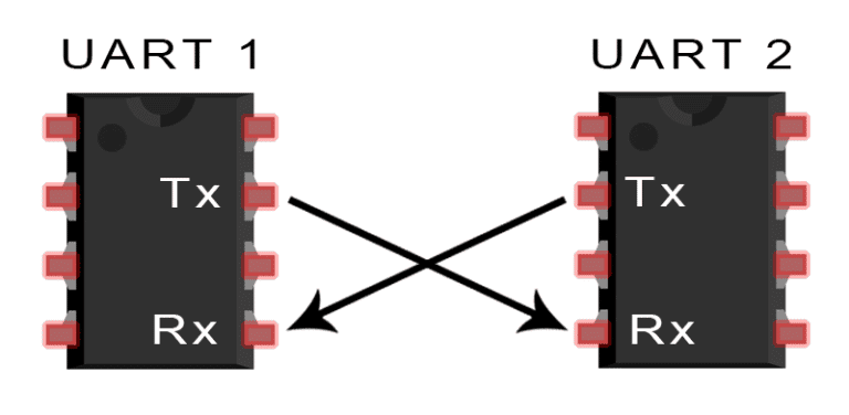
UART
Only two wires are needed to transmit data between two UARTs. Data flows from the Tx pin of the transmitting UART to the Rx pin of the receiving
UART.
UARTs transmit data asynchronously, which means there is no clock signal to synchronize the output of bits from the transmitting UART to the
sampling of bits by the receiving UART. Instead of a clock signal, the transmitting UART adds start and stop bits to the data packet being
transferred. These bits define the beginning and end of the data packet so the receiving UART knows when to start reading the bits.
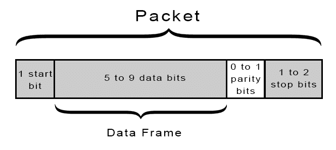
UART transmitted data is organized into packets. Each packet contains 1 start bit, 5 to 9 data bits (depending on the UART), an optional parity bit, and 1 or 2 stop bits:
Comparison table between I2C, SPI and UART
| Protocol | Characteristics | Advantages | Disadvantages |
|---|---|---|---|
| I2C |
|
|
|
| SPI |
|
|
|
| UART |
|
|
|
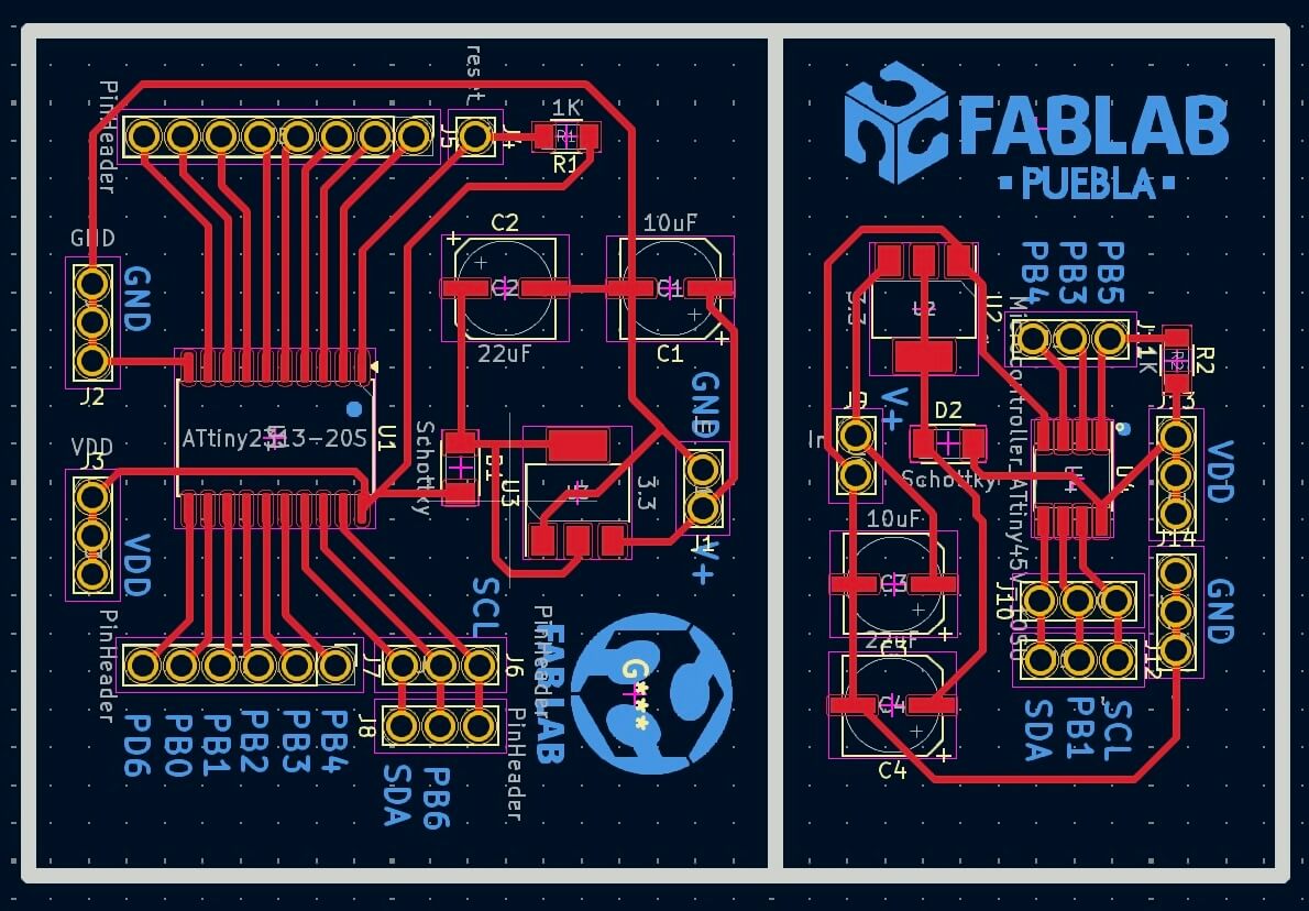
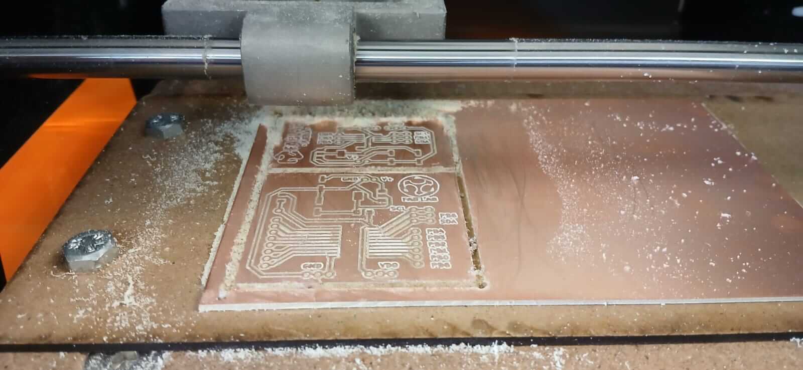
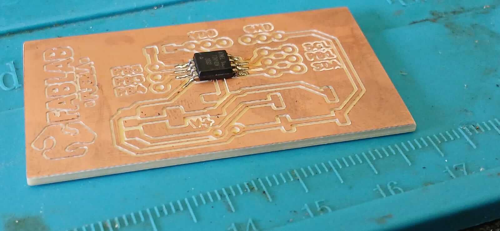
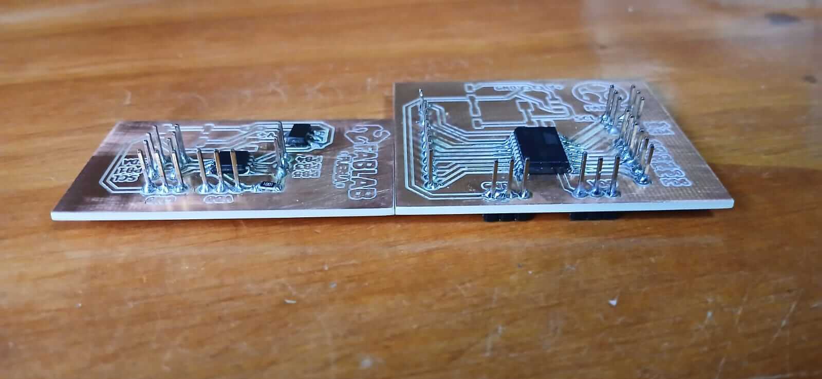
New boards Attiny 45/2313
It was decided to make two new boards, with the goal of practicing using the "ATtyni45" and the "ATtiny2313" along with the XIAO RP2040 designed during the " 8.- Electronics Production ". week. The datasheets for the ATtinys are shown in the following links.
The following images show the schematic and layout designs.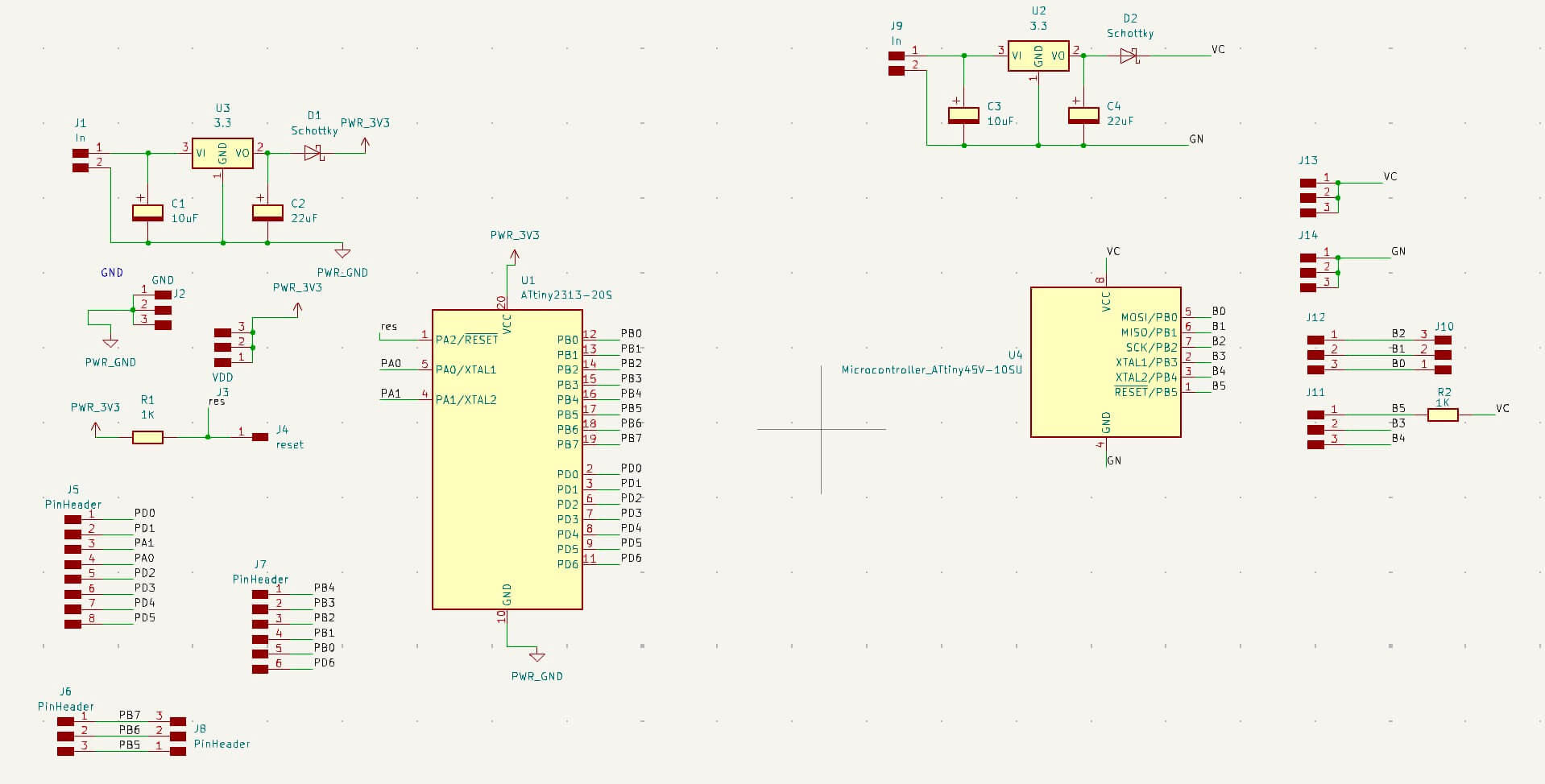
The machining and solding process is shown below.
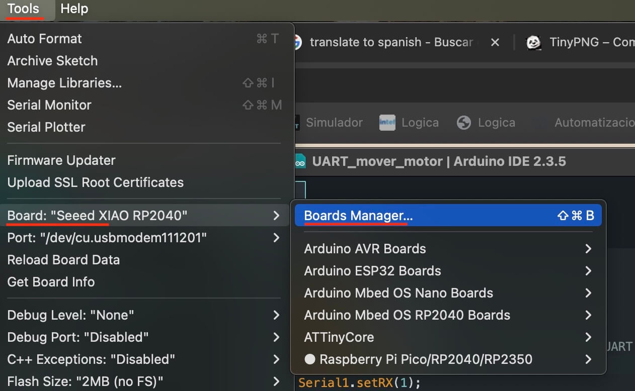
FIRST STEPS WITH ATTINY
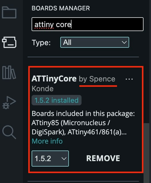
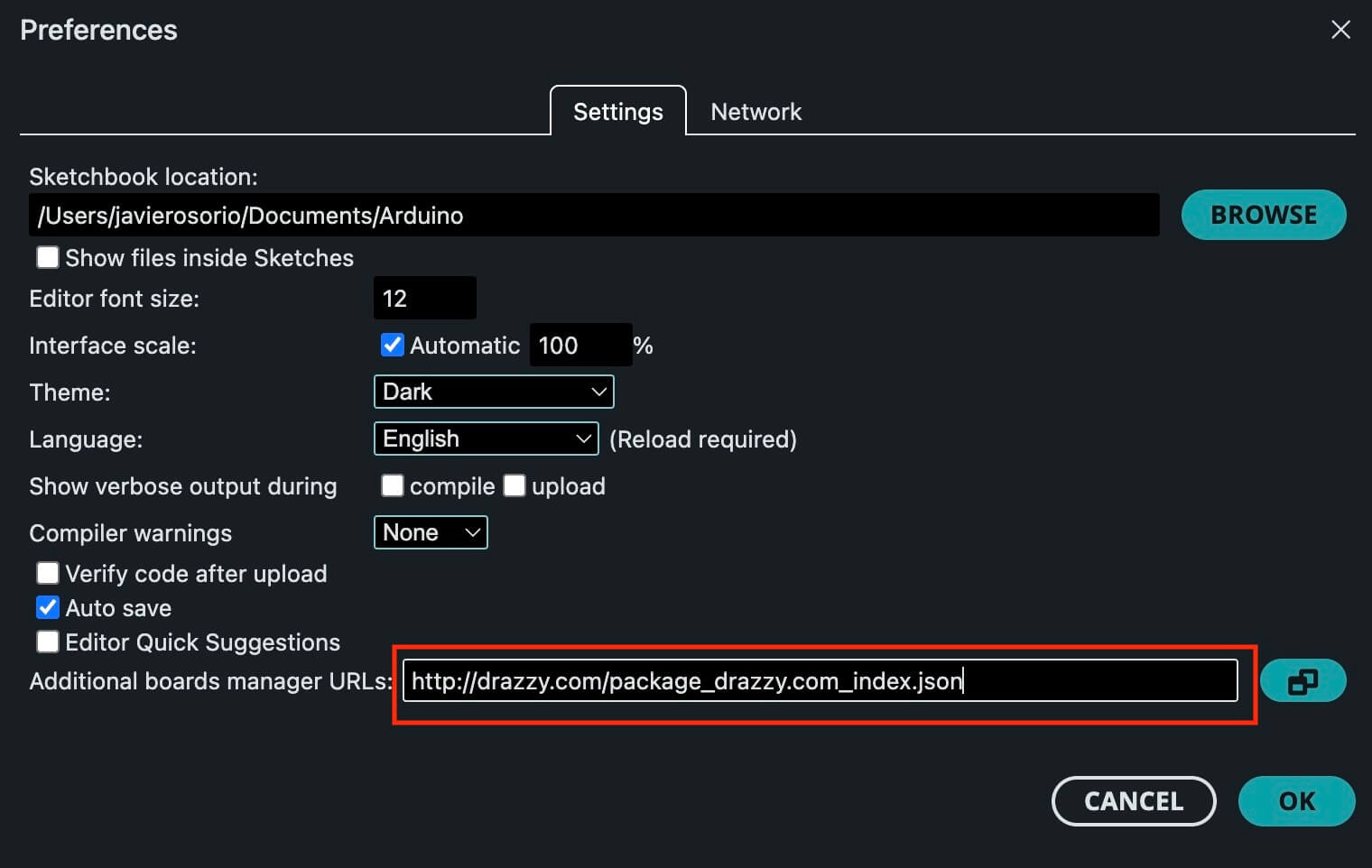
To start, it is important to download the “ATtiny boards”, to do this go to "Tools - Board - Boards Manager...".
Programmer
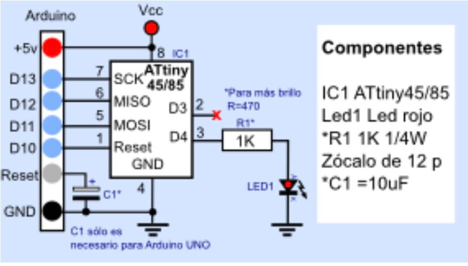
One of the drawbacks we have when working with "ATtiny" is that we need another board to be able to load the program onto it. In our case, we will use the "Arduino UNO" and follow the following diagram.
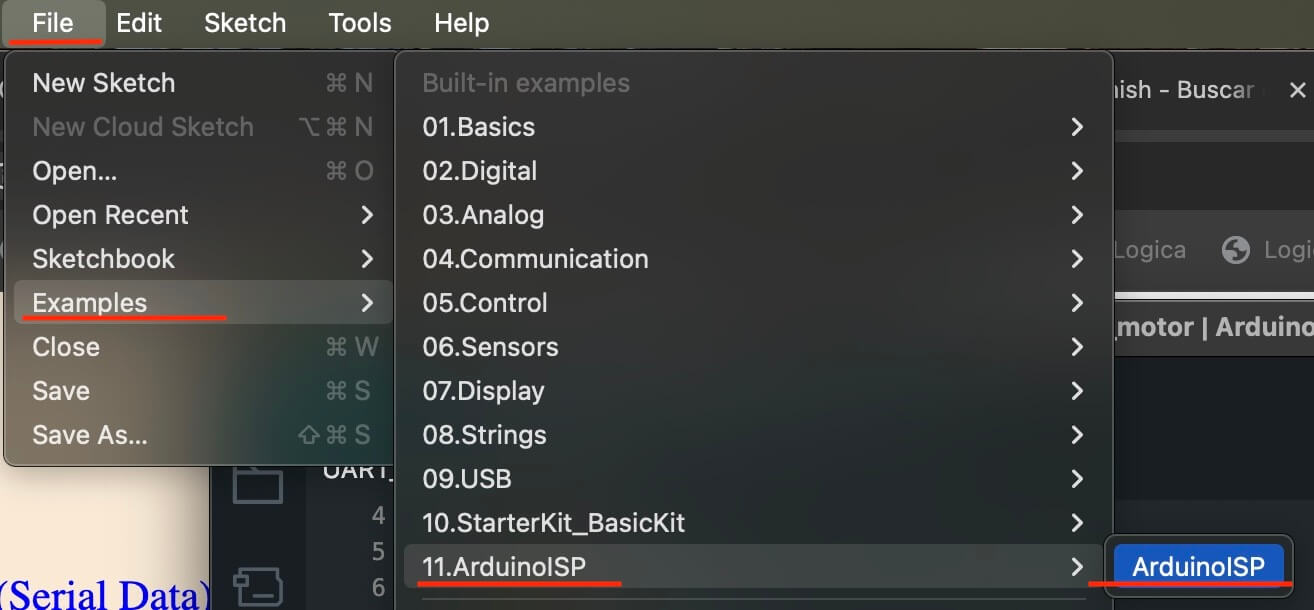
Without connecting the \(10 \mu F\) capacitor to the Arduino, we go to "File - Examples - ArduinoISP - ArduinoISP", and load the Arduino to be able to use it as a programmer.
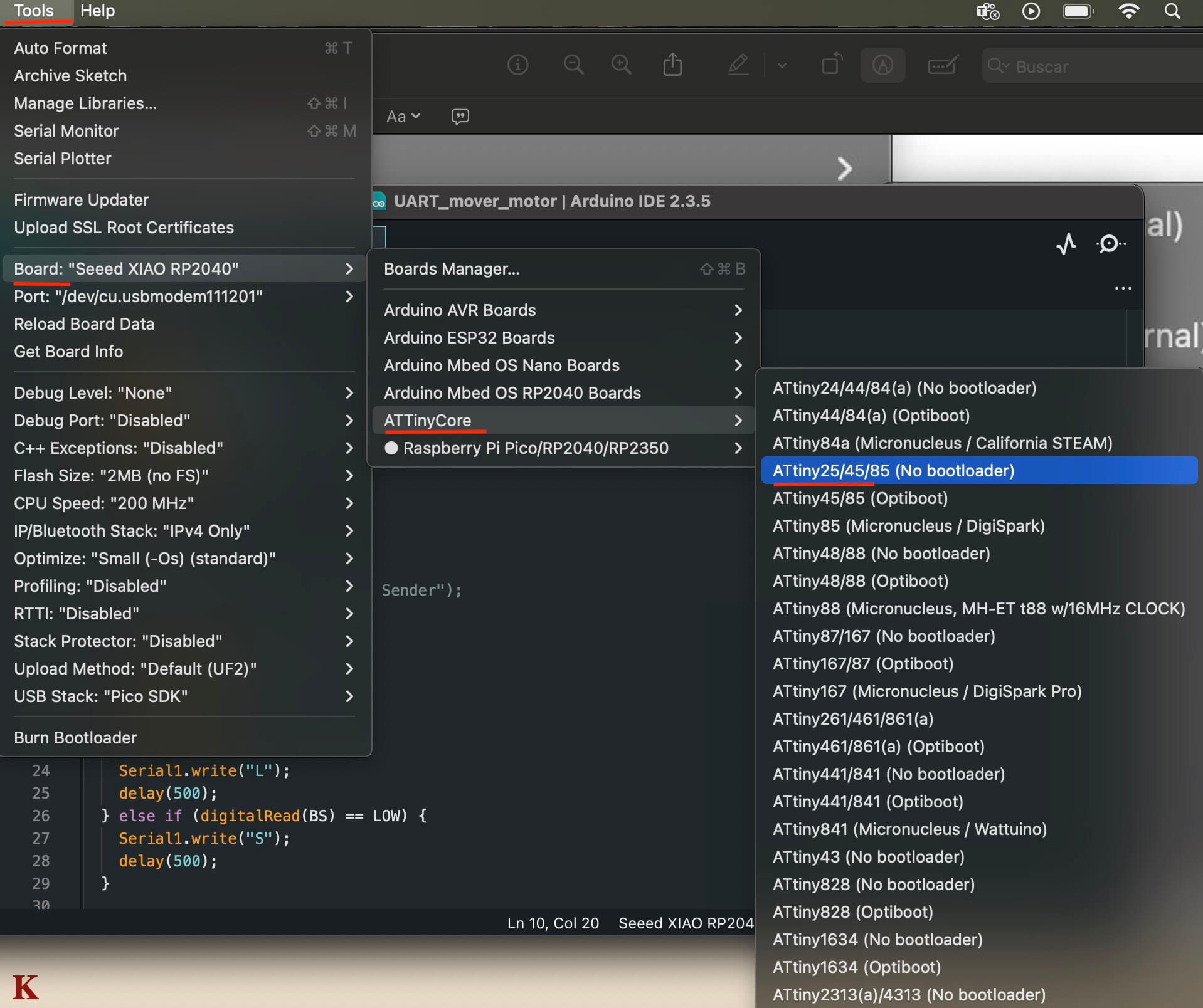
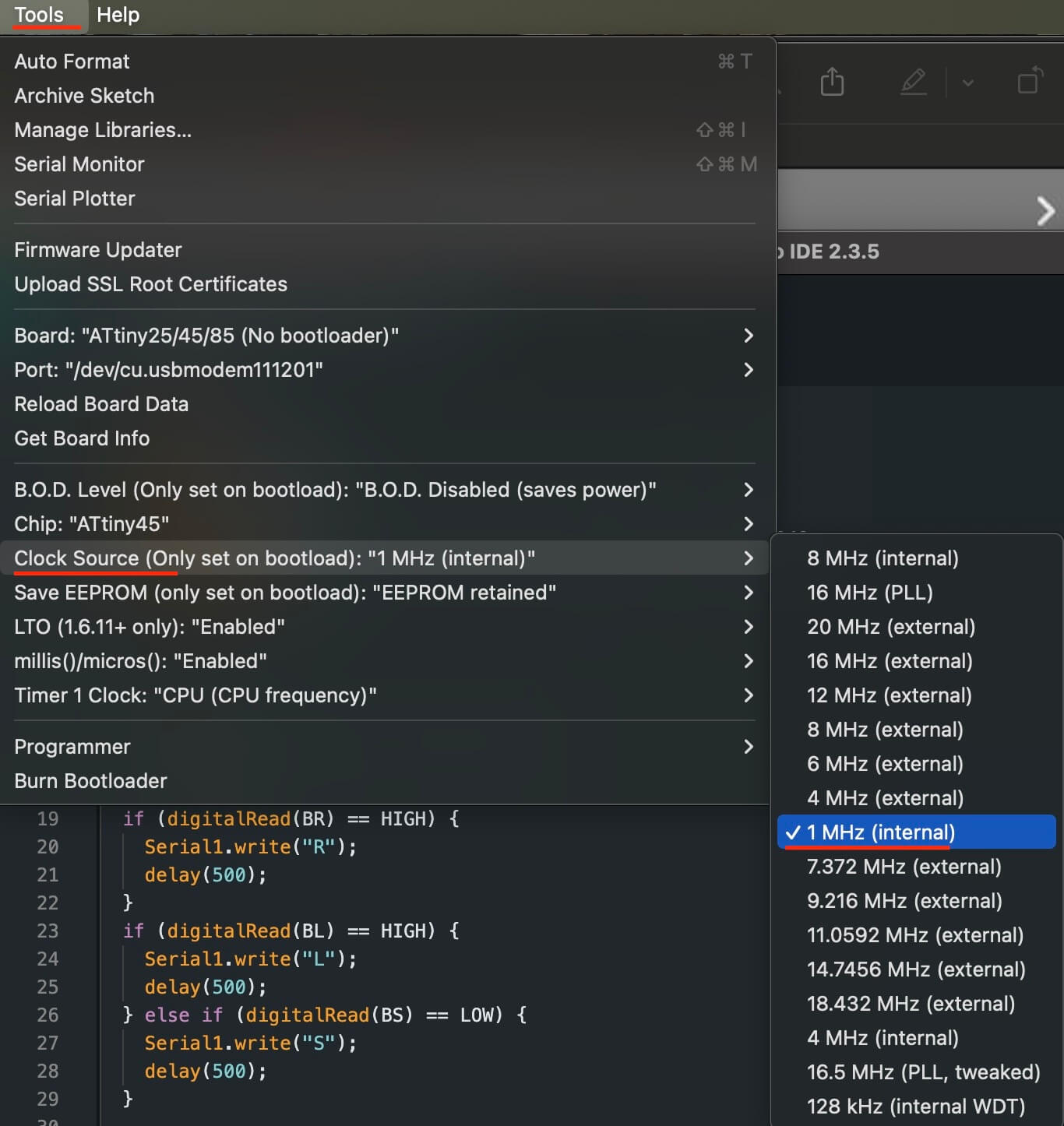
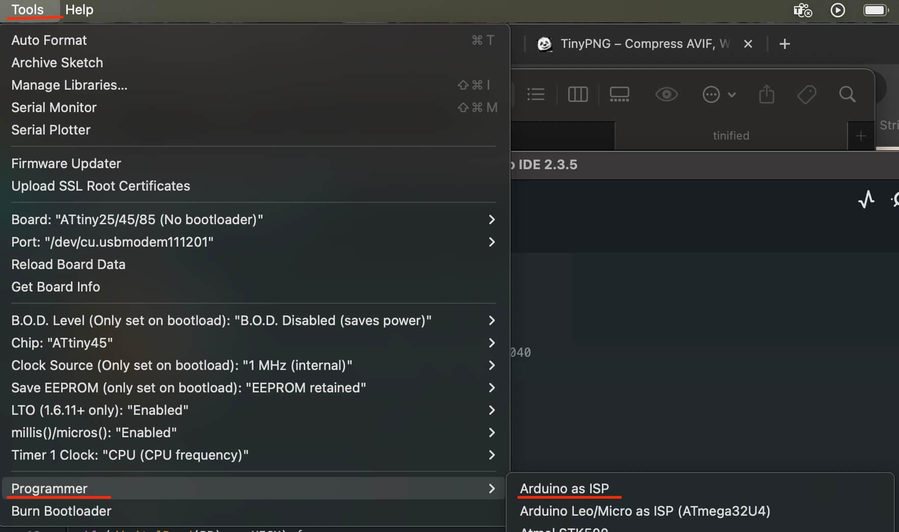
When the Arduino has been loaded as a programmer, we proceed to open and load the program corresponding to “ATtiny". To do this, we need to select the “ATtiny” board we will be using. Once the “ATtiny” is configured, we go to "Tool - Programmer" and select "Arduino as ISP". With this step is completed, we can "Upload" the program.
Code
I2C
One of the biggest problems we had was that when trying to communicate with "ATtiny" via "I2C", "ATtiny" could not be recognized, so searching in the web it was recommended to install the "TinyWire" package, for that the .zip that appears in the following link was downloaded.
Once you've downloaded the .zip, we recommend saving it into the "Arduino" libraries folder in your home directory (if you don't have one, create a new one in Arduino). After that, go to "Sketch - Include Library - Add .ZIP Library..." and add your "TinyWireS-master.ZIP" file.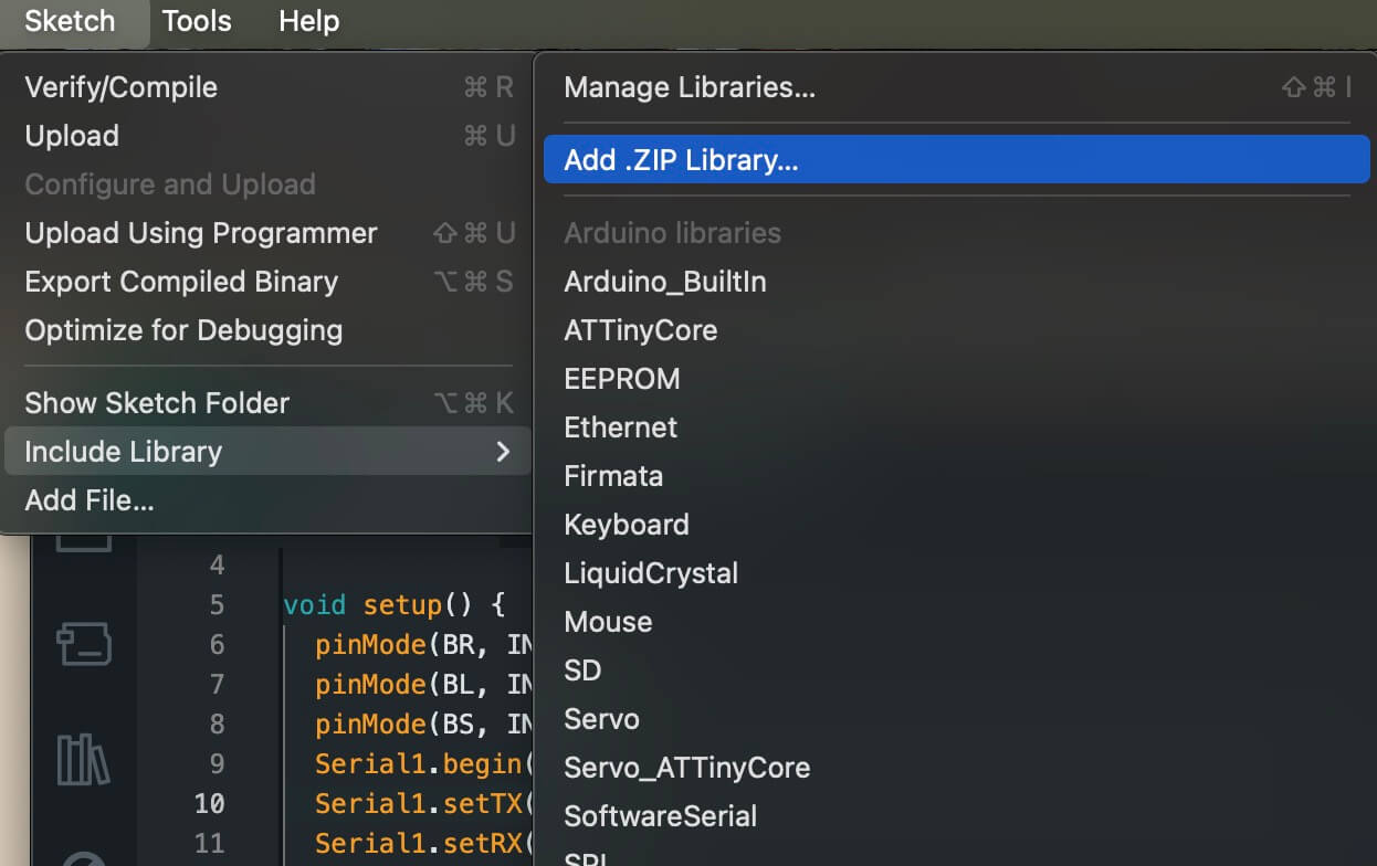
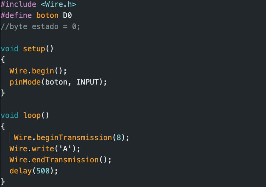
The first thing we do is use the "Wire.h" library, in the "void setup," and we must start the "Wire" using the "Wire.begin();" instruction. In the "void loop()," we begin the transmission to the "secondary" 8; where we send an 'A' and end the transmission.
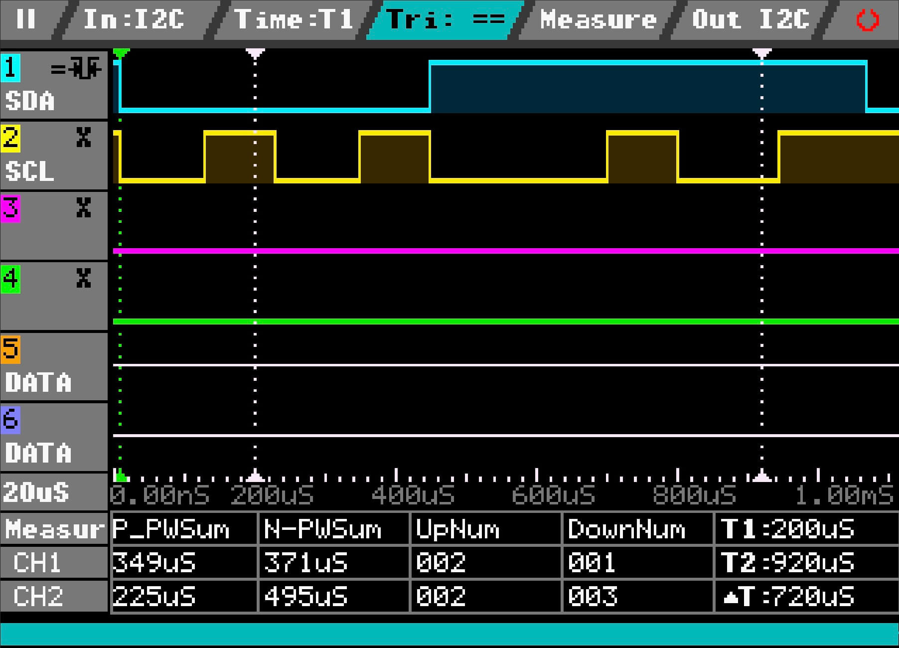
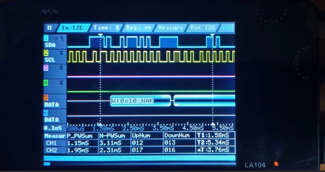
To observe I2C communication, the "LA104 Logic Analyzer" was used; below are the images from the analyzer, as well as the link to the manual.
To test the functionality and see if communication existed, the following program was created on the "ATtiny45." The first thing you see in
the code is the "#include < TinyWireS.h >"file. Note that it begins with "Tiny," indicating that it's an "ATtiny," and ends with an "S,"
indicating that the program was created for the "secondary" ATtiny..
Inside the "void setup()" we have two important instructions.
- TinyWireS.begin(I2C_SLAVE_ADDRESS); An address is assigned to the secondary.
- TinyWireS.onRequest(requestEvent); In response the secondary makes us go to the "requestEvent" function
SPI
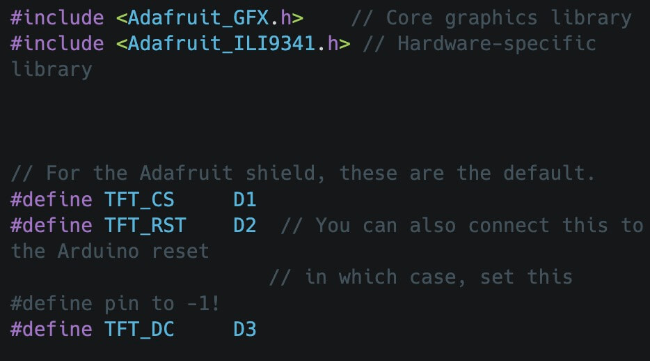
In this section, we'll be using the ILI9341 TFT display connected to the XIAO RP2040. Information on connecting the display to the XIAO can be found at the following link.
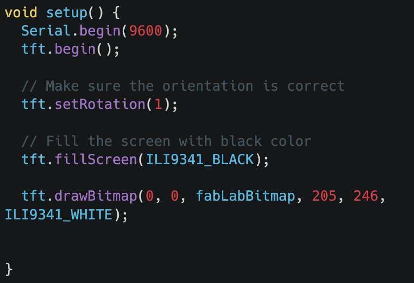
What we're looking for is to generate images on the screen, so we need to create a bitmap. A good way to create them is with image2cpp , which is a simple tool for converting images into byte arrays.To begin, it is important to declare the "Adafruit" libraries, as well as define the "CS", "RST" and "DC" pins.
Inside the "void setup()" section, we initialize the serial port and the TFT. In this section, we set the initial parameters for the TFT display and place a created "Bitmap" image.
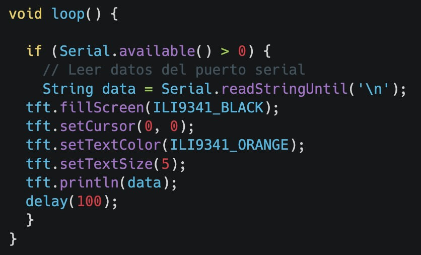
Inside the "void loop()", we wait for some input on the serial port, the value of which will be displayed on the OLED screen.
The complete code is shown below.
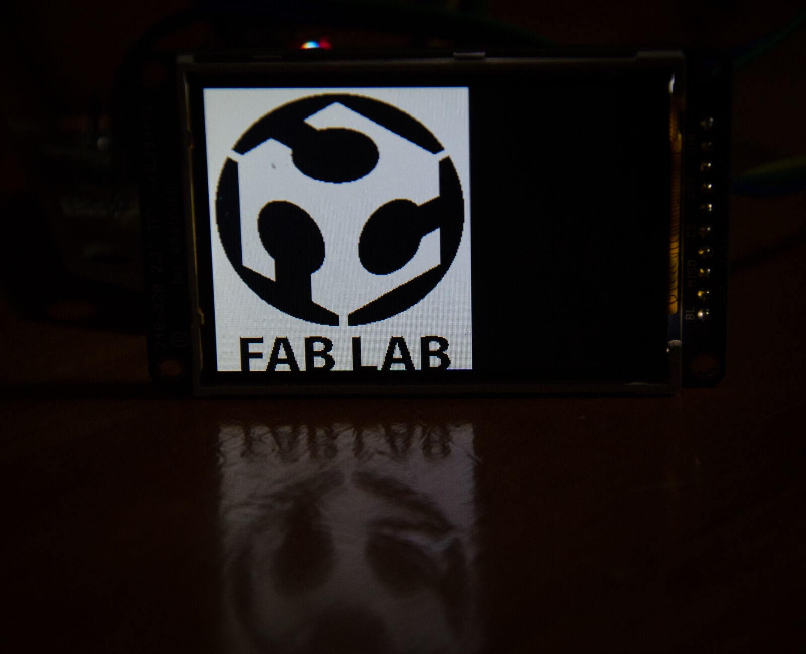
The results can be seen below.
Learning outcome
This week we learned the importance of communication between devices. While there are many communication protocols, it's important to understand their pros and cons, as well as the limitations of our own microcontrollers. As for the ATtiny, although it's a very efficient and compact microcontroller, its limited compatibility with certain libraries and tools can be a challenge when it comes to specific applications.