week8. Electronics Production
Assignment
Group assignment
- characterize the design rules for your in-house PCB production process
- submit a PCB design to a board house
Individual assignment
- make and test a microcontroller development board that you designed
- extra credit: make it with another process
Group assignment
For more information about group projects, please see the group project page on the FabLab Kannai website.
Group assignment page is here
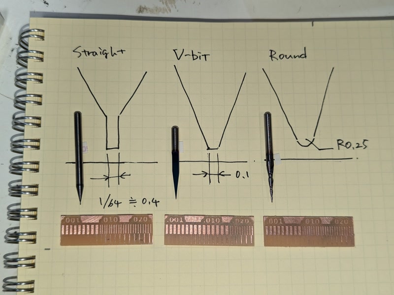
In the environment of FabLab Kannai, the V bit 30 degree End Mill was the most accurate of the following three End Mills, and it was able to cut the copper printed circuit board material.
| 1/64 Straight bit | V bit 30 degree | R0.25 Ball-nose tapered |
|---|---|---|
| Traces thicker than 0.12mm are retained | Traces thicker than 0.07mm are retained | 0.10~0.16mm traces are gradually removed |
| A little burr occurred (may be due to wear) | Almost no burrs occurred | A large amount of burrs occurred though it was new |
| Good | Great 👍 (At least while new) | Not suit for PCB milling |
Thank you, Naoki Hayashi-san!
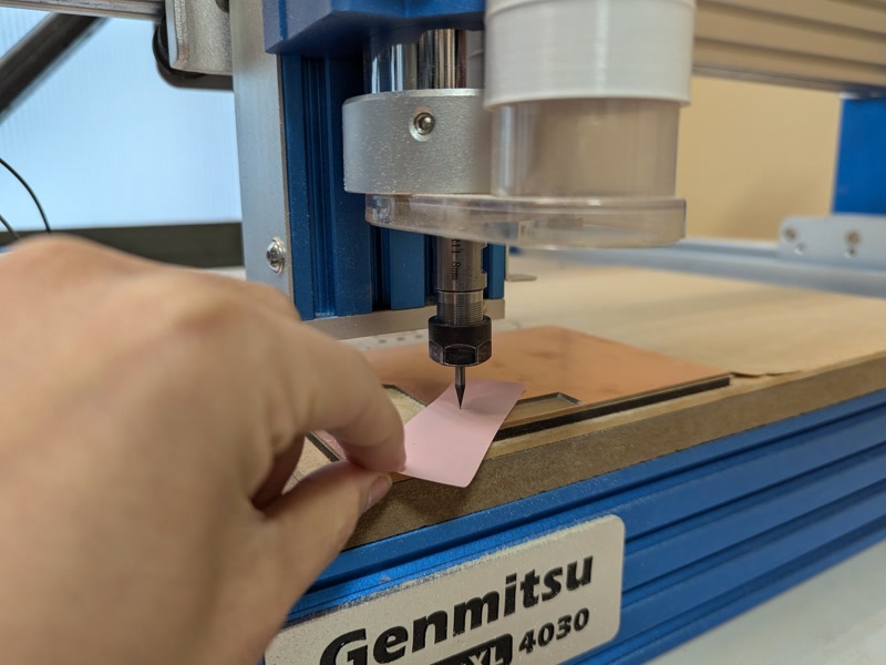
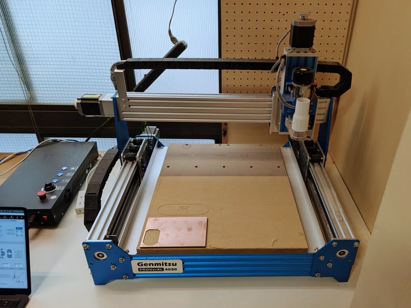
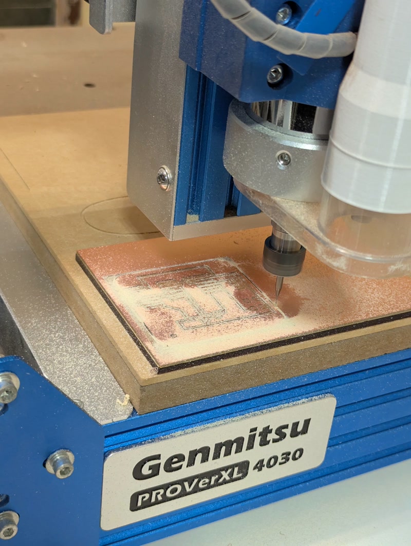
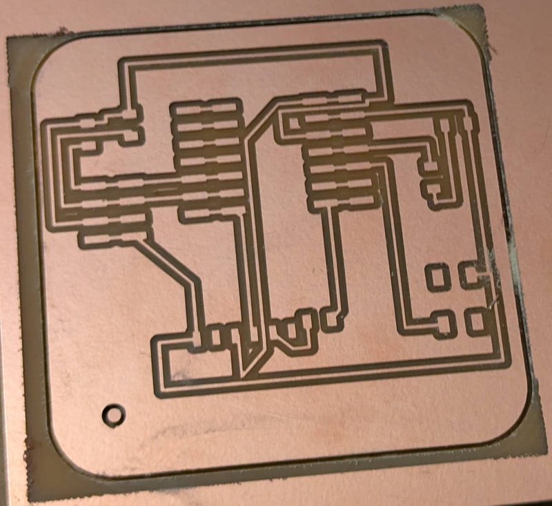
PCB board manufacturing
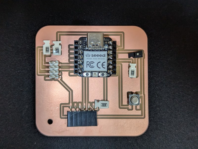
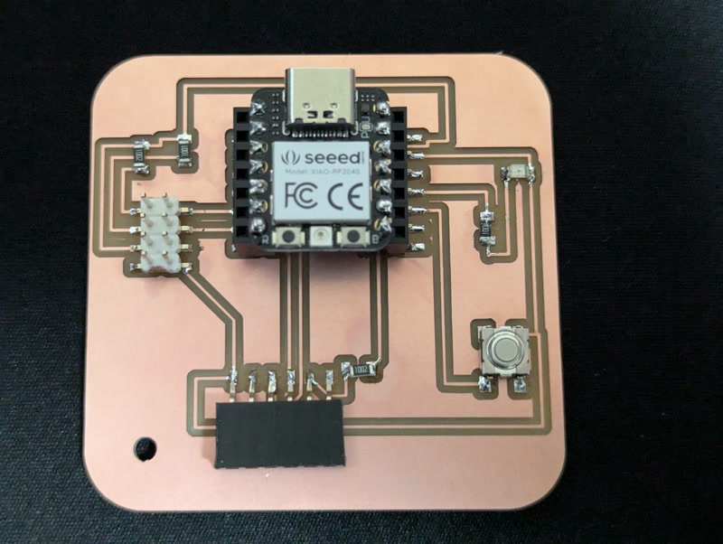
The process of cutting the PCB board to create the microcontroller development board for FabLab Kannai in the Individual assignment was carried out using a CNC router Genmitsu PROVerXL 4030.
Creating data for milling
Using the electronic circuit created in week06, we used Fusion Electronics to create the data for milling. It is necessary to create each file according to the type of cutting work for the CNC router.
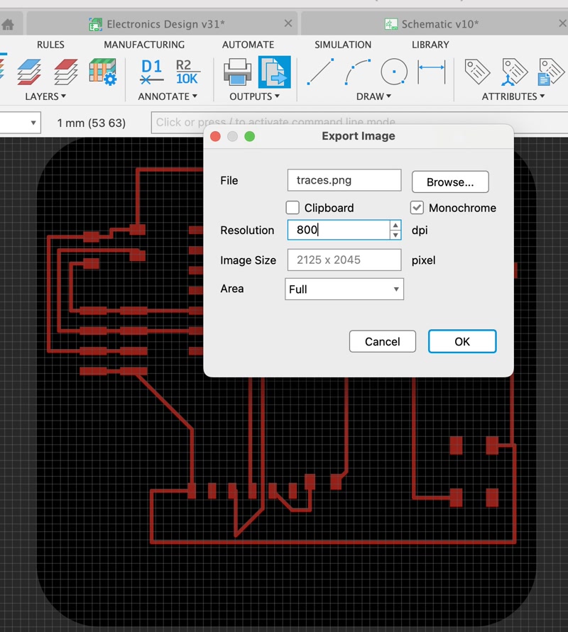
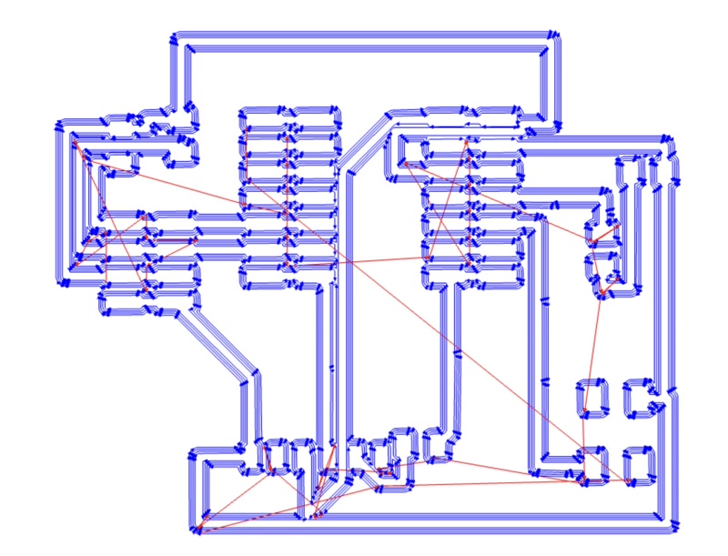
- traces.png: Data for creating circuits by shaving the copper on the surface of the board
- millholes.png: Data for holes that penetrate all the way to the bottom of the circuit board
- outline.png: Finally, the data for cutting out the outline of the PCB
Creating traces.png
Create a new layer called “RawPCB” in the right panel.
Draw a rectangle that is slightly larger than the entire circuit.
Display only the layers you need.
Adjust the “SELECTION FILTER” so that unnecessary shapes such as “+” are not displayed.
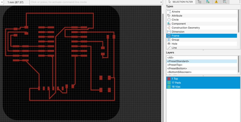
Export as traces.png.
- Documents > Print > Export
- Check “Monochrome”
- Resolution: 800dpi
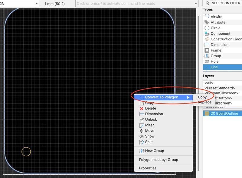
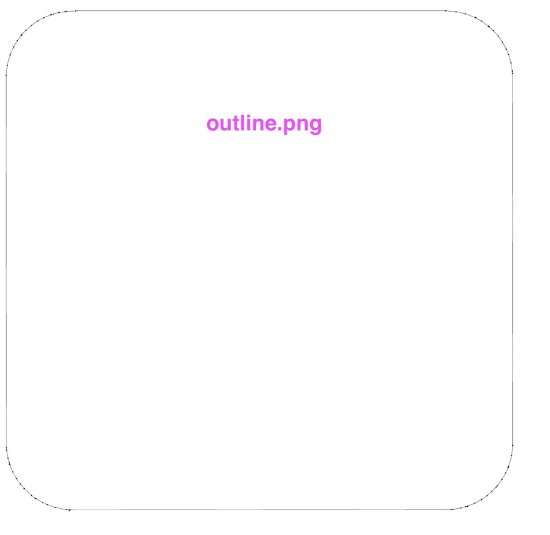
Create outline.png
- In the right panel, display only the “BoardOutline” layer.
- In the “SELECTION FILTER”, select Type: “Line”.
- Select all (Ctl+A).
- Right-click to select “Covert To Polygon”, then select “Copy” > “MillOutline”.
- In the right panel, display only the “MillOutline” layer.
- Export as outline.png.
Creating millholes.png
- Create a new layer called “MillHoles” in the right panel.
- Display only the “BoardOutline” layer.
- In the “SELECTION FILTER”, select Type: “Circle”.
- Select all (Ctl+A).
- Measure the diameter of the millhole (3.2mm).
- Select the tab “DOCUMENT” > “Grid Settings” and change the “Grid Size” to 1mm.
- Set the “Hole Drill” to the diameter (3.2mm) size.
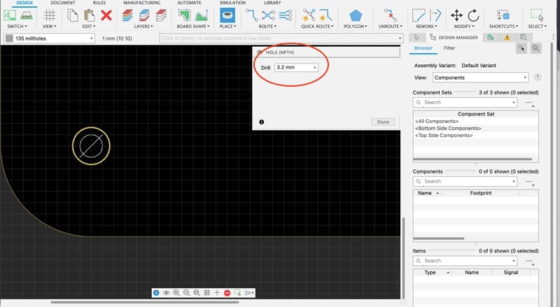
- Place a Circle on the MillHole.
- Select the tab “AUTOMATE” > “Run ULP” and set “drill-aid” to 0.
- In the right panel, display only the layer “centreDrill” created in the previous operation.
- Change the color of the layer “centreDrill” to gray.
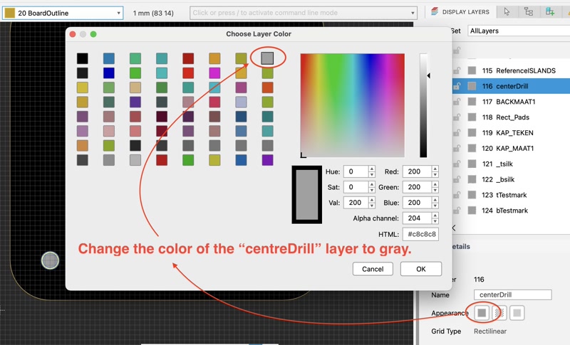
- Export as millholes.png.
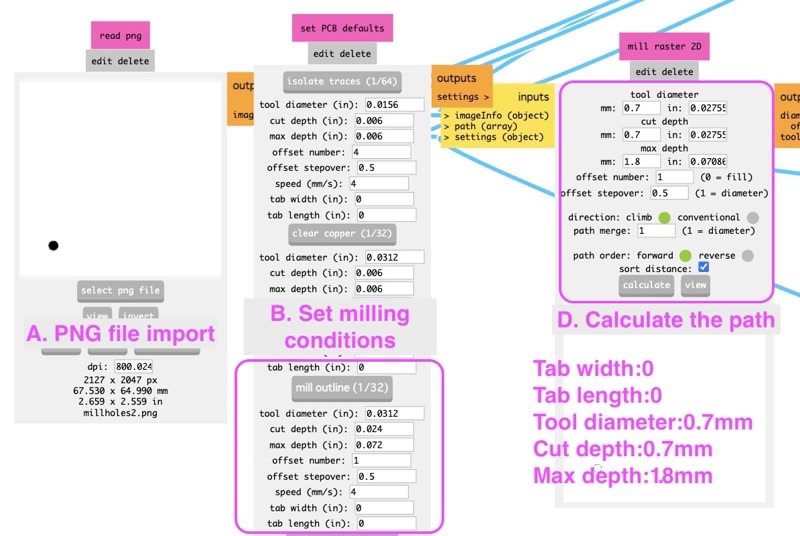
Creating G-code with Mods
Use the mods G-code generator to create G-code.
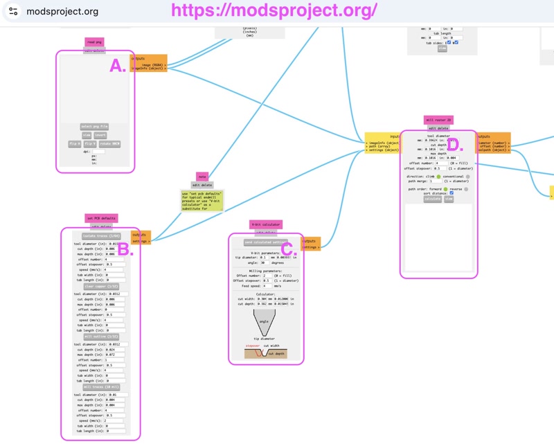
Right-click on the white canvas and select Program > Open program > machines > G-code > mill 2D PCB.
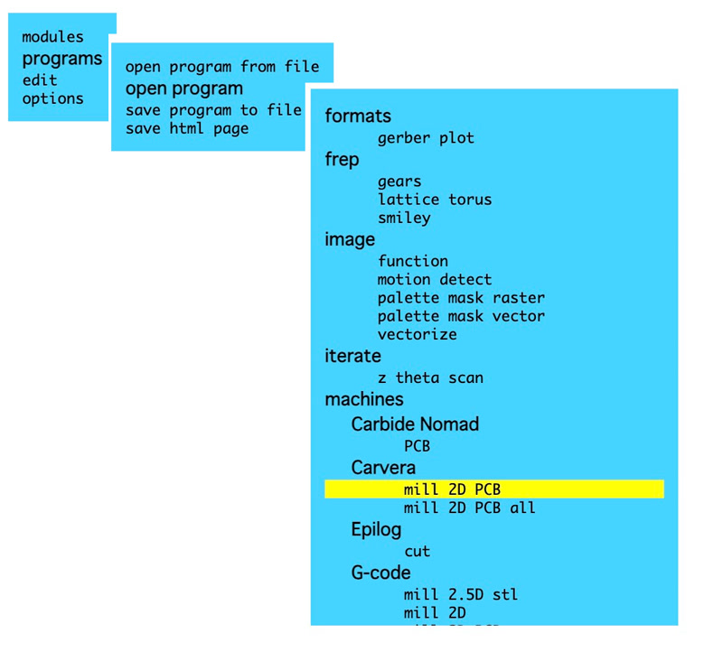
The structure of the "Mill 2D PCB" page is as follows.
- A.: Read PNG
- B.: Set PCB defaults
- C.: V-bit calculator(if you use V-bit)
- D.: Mill raster 2D
Milling the Traces
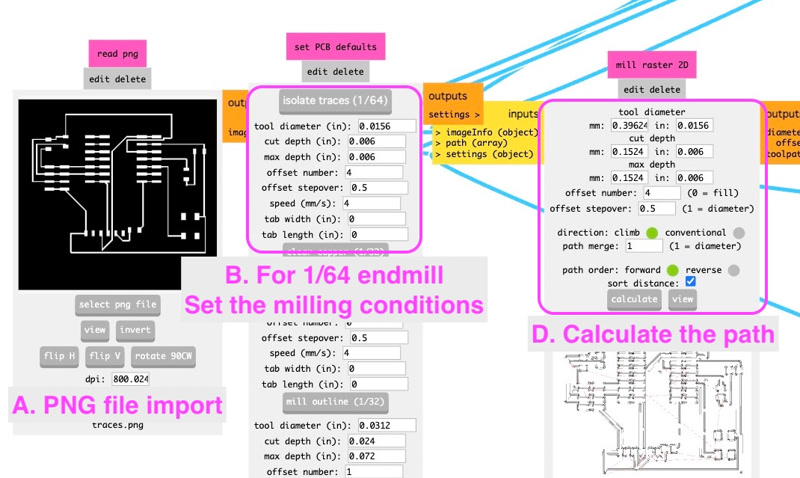
Milling the Interior
When you load millholes.png, click the “invert” button to reverse the black and white.

G-code file
The following is the G-code file we created this time.
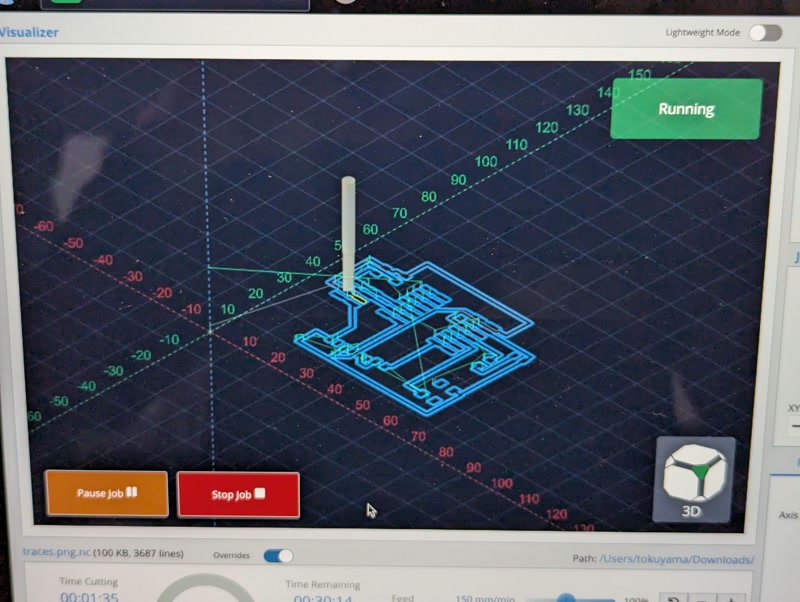
Controlling a CNC router with G-Sender
The PCB boards are milled using the CNC router Genmitsu PROVerXL 4030 based on the G-code created by GSender.
GSender Settings
- Start GSender: Start the software and wait until the CNC router is recognized.
- Check the connection:
- Click the “Connect” button.
- Select the connected port and click “Connect”.
- Secure the material:
- Secure the material firmly to the workbench. Use double-sided tape.
- Set the home position:
- Set the initial position of the CNC router using the “Zero X” and “Zero Y” buttons.
- Place a piece of paper between the material and the End Mill, and lower the End Mill until the paper stops moving, then lower it a further 0.1mm.
- Set the initial position of the Z-axis using “Zero Z”.
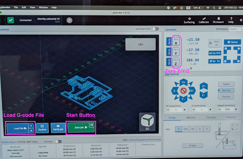
Start milling
- Import G-code file:
- Select “Open File” to load the G-code to be used for the machining.
- Preview check:
- The G-code preview will be displayed, so check the working range and cutting depth.
- Set speed and progress:
- Adjust the cutting speed and spindle speed in the “Settings” menu.
- Start cutting:
- Press the “Start” button to begin milling.
- While cutting, check the CNC router's operating status and remaining time on the GSender screen.
WARNING
If you do not pay attention to the following points before starting the milling process with GSender, the milling process may stop partway through.
- Close any other applications other than GSender.
- Connect the power supply and set it so that it does not go into sleep mode.
- Use the official USB adapter.
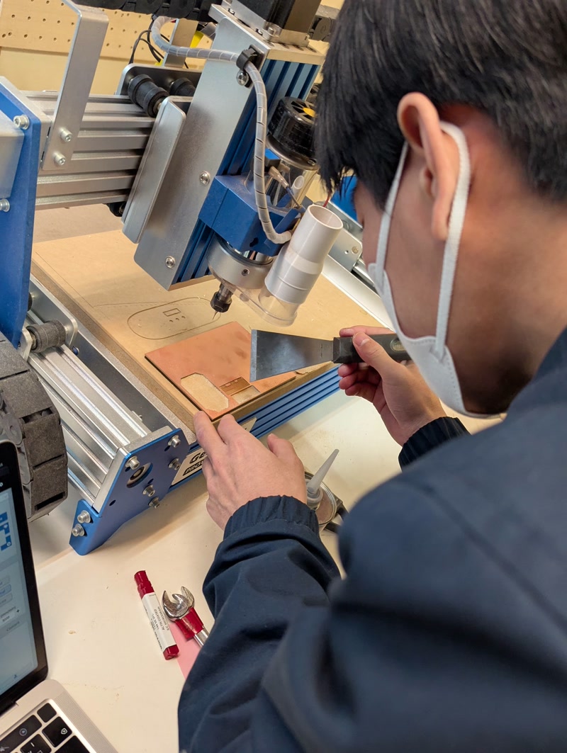
Soldering components to the PCB board
Solder the components to the PCB board using surface mounting.
Preparing the work environment
- Organize the workbench and make sure you have enough space to fix the components and the board in place.
- Ensure good ventilation so that you don't inhale any fumes from the solder.
- Set the soldering iron to the appropriate temperature (usually around 300℃ to 350℃).
- Clean the tip of the soldering iron with a sponge or cleaner to remove any oxides.
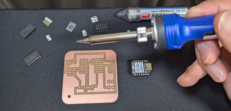
Part positioning
- Place the parts in the corresponding locations on the board.
Soldering
- Put a small amount of solder on one of the lands on the circuit board in advance.
- Grab the chip component with tweezers and place it in the correct position (as close to the center of the pattern as possible).
- Hold the component in place with tweezers, and hold the soldering iron in the other hand to temporarily fix the side with the pre-applied solder.
- Join the other side of the component to the soldering iron and solder.
- Reheat the temporarily fixed side to finish the soldering.
Programming
Connect the soldered PCB board to a USB cable, and use the development environment Thonny to program in the programming language MicroPython. The aim is to make the LED on the PCB board light up only when the tact switch is pressed.
Installing the firmware
Upload the latest MicroPython firmware (RPI_PICO-20241129-v1.24.1.uf2) to the XIAO RP2040. Download the firmware from the official website, and write it to the RP2040 in boot mode.
TIP
Uploading using Finder didn't work, but uploading the firmware using the cp command from the terminal did work.
MicroPython code
The LED is turned on only when the tact switch is pressed.
from machine import Pin

# Pin settings
button = Pin(4, Pin.IN, Pin.PULL_UP)  # Tact switch: pull-up resistor enabled
led = Pin(3, Pin.OUT)                 # LED: Output mode

while True:
    if button.value() == 0:  # When the switch is pressed (LOW)
        led.value(1)         # Turn on the LED
    else:
        led.value(0)         # Turn off the LED
You can see that the LED in the lower left corner is lit up only when the tact switch is pressed.
Afterthoughts
It's a great feeling of accomplishment to make your own PCB board. I was really impressed.
It was difficult to solder the surface mount components on the PCB board. My fingers shook.