week6. Electronics Design
Assignment
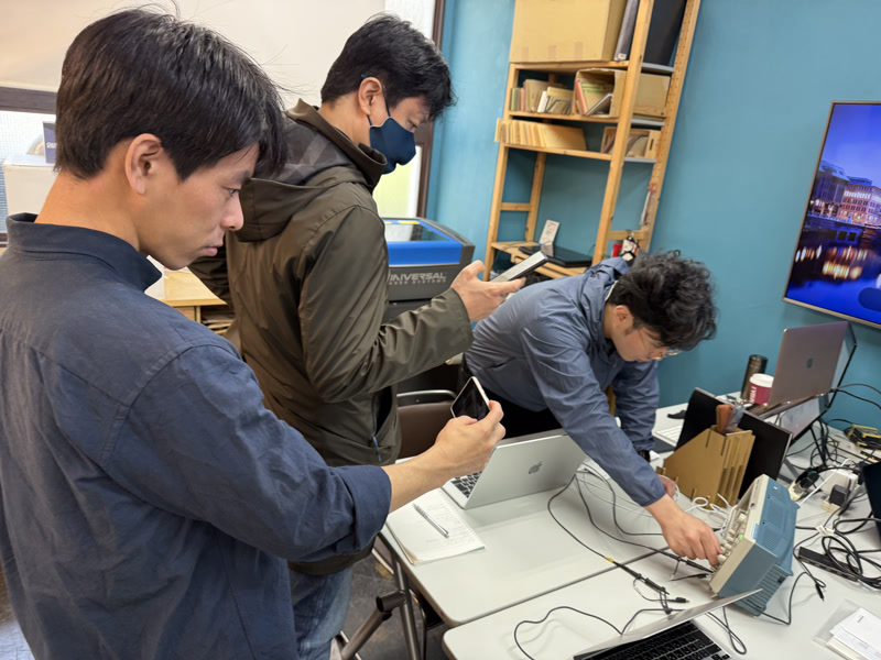
Group assignment
- use the test equipment in your lab to observe the operation of a microcontroller circuit board
Individual assignment
- use an EDA tool to design a development board that uses parts from the inventory to interact and communicate with an embedded microcontroller
- extra credit: try another design workflow
- extra credit: simulate your design
- extra credit: design a case around your design
Group assignment
For more information about group projects, please see the group project page on the FabLab Kannai website.
Group assignment page is here
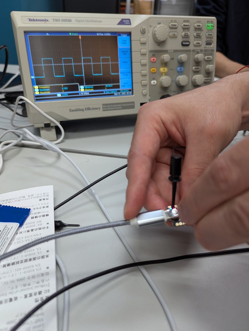
The above photo shows the waveform of the oscilloscope when the following code is executed. It is a clean waveform with no noise.
from machine import Pin, PWM
import time

# Output pin (GPIO of RP2040)
PWM_PIN = 7

# PWM initialization
pwm = PWM(Pin(PWM_PIN))
pwm.freq(50000)         # Set the PWM frequency to 50 kHz.
pwm.duty_u16(32768)     # 50% duty cycle (range 0-65535) in 16-bit values

while True:
time.sleep(1) # Maintains PWM signal in an infinite loopThe above video shows the waveform of an oscilloscope when the following code is executed. The ratio (duty cycle) of the “on time” and “off time” of the PWM signal changes depending on the change in the PWM (pulse width modulation) signal. This shows that the width of the signal is changing and that noise is being generated.
import math
from machine import Pin, PWM
import utime

# Output pin
PWM_PIN = 7

# Sampling rate and frequency settings
SAMPLE_RATE = 50000  # 50kHz
WAVE_FREQ = 1000  # 1kHz sine wave

# PWM resolution (maximum for RP2040 is 16 bits)
PWM_RES = 256

# Sine Wave Table Generation (256 Samples)
sine_wave = [int((math.sin(2 * math.pi * i / 256) + 1) * (PWM_RES // 2)) for i in range(256)]
print(sine_wave)

# PWM initialization
pwm = PWM(Pin(PWM_PIN))
pwm.freq(SAMPLE_RATE)
pwm.duty_u16(0)

# Outputs a sine wave
index = 0
while True:
    pwm.duty_u16(sine_wave[index])
    index = (index + 1) % 256
    utime.sleep_us(int(1e6 / WAVE_FREQ / 256))
EDA tool
At FabLab Kannai, we used Fusion Electronics to design circuits.
Schematic design
Select “New Electronics Design” from the menu to start Schematic design.
Basically, four files are created.
- Electronics design: A design file created by integrating various elements related to electronic circuit design.
- Schematics: A conceptual diagram of an electronic circuit that does not include the specific placement of actual components.
- PCB layout: A design (2D drawing) that physically arranges electronic components on a circuit board.
- 3D PCB design: A design file that creates a 3D version of a PCB layout.
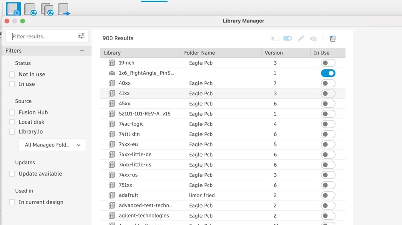
Register the necessary libraries
Select “Library” > “Open Library Manager” from the menu to open the Library Manager. Download and import the necessary libraries in the Library Manager and register them. The required libraries were based on the fab library in the fab inventory.
TIP
Please note that you will not be able to register the library in the design screen until you turn on the “In Use” switch after importing it.
Component layout
Select the required components from the “Component Placement” menu and add them to the design screen.
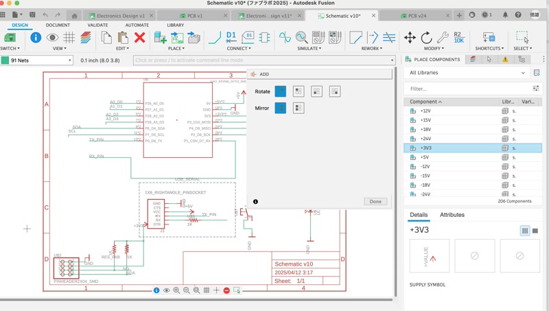
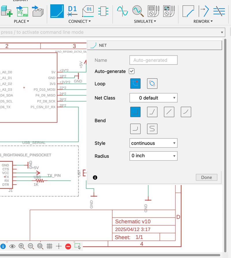
Next, connect the parts. I used the “Net” tool to draw a green line to connect the parts. Please check that each part is securely connected by the green line.
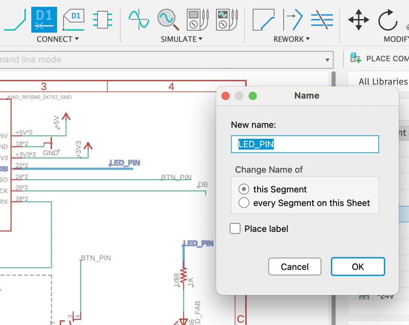
I used “Name” to give a name to the green wire used to electrically connect the components.
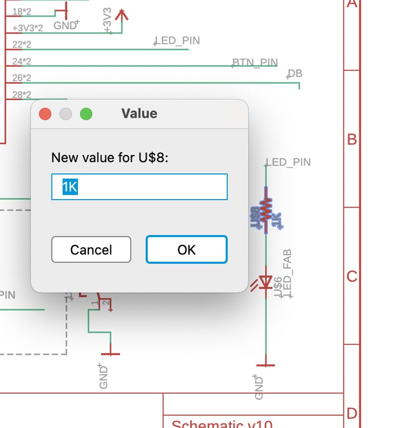
I used “Value” to add value to income components such as resisters.
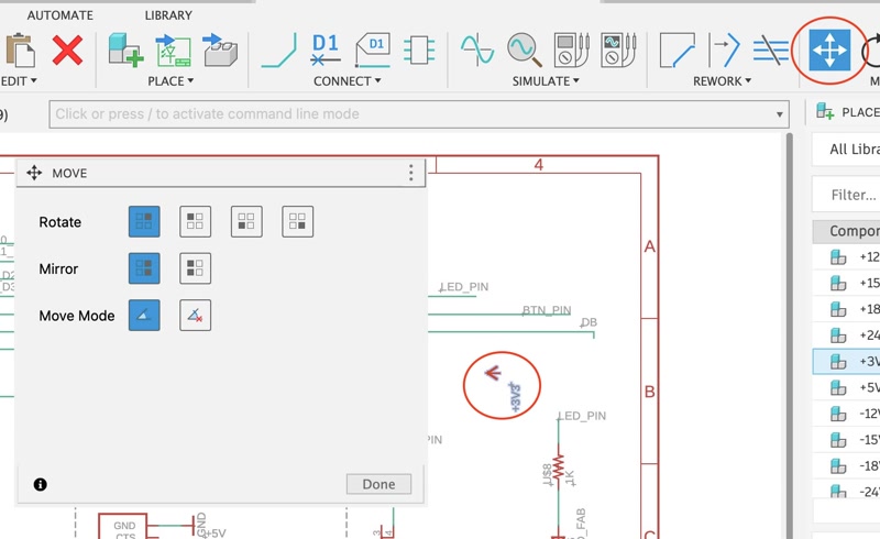
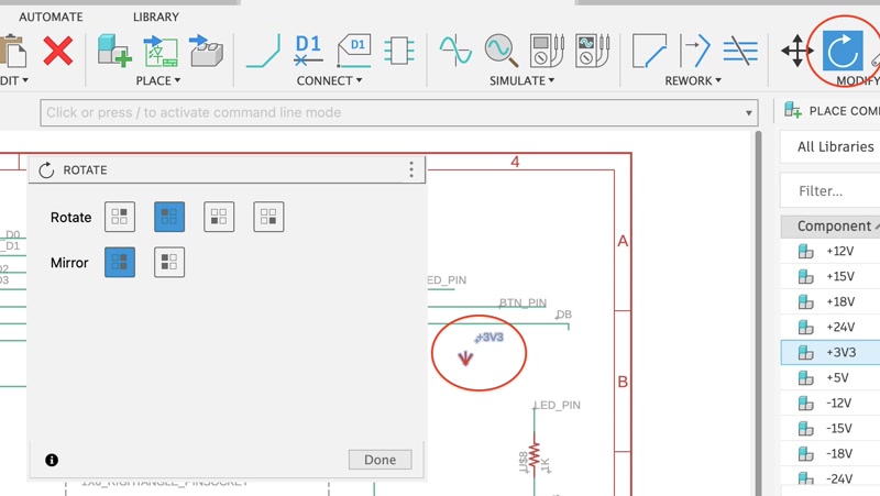
I used “Move” and “Rotate” to place symbols and green lines where they should be.
PCB Layout
Select the “Switch” icon in the top left corner of the menu to switch to “PCB Document” mode.
Setting design rules
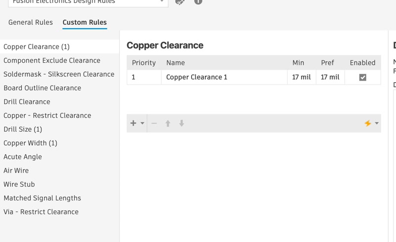
Set the rules as follows in the “Rules” > “Design Rules” > “Custom Rules” tab of the menu.
- Copper Clearance: 17 mil
- Drill Size: 0.8 mm
- Copper Width: 16 mil
Create a path
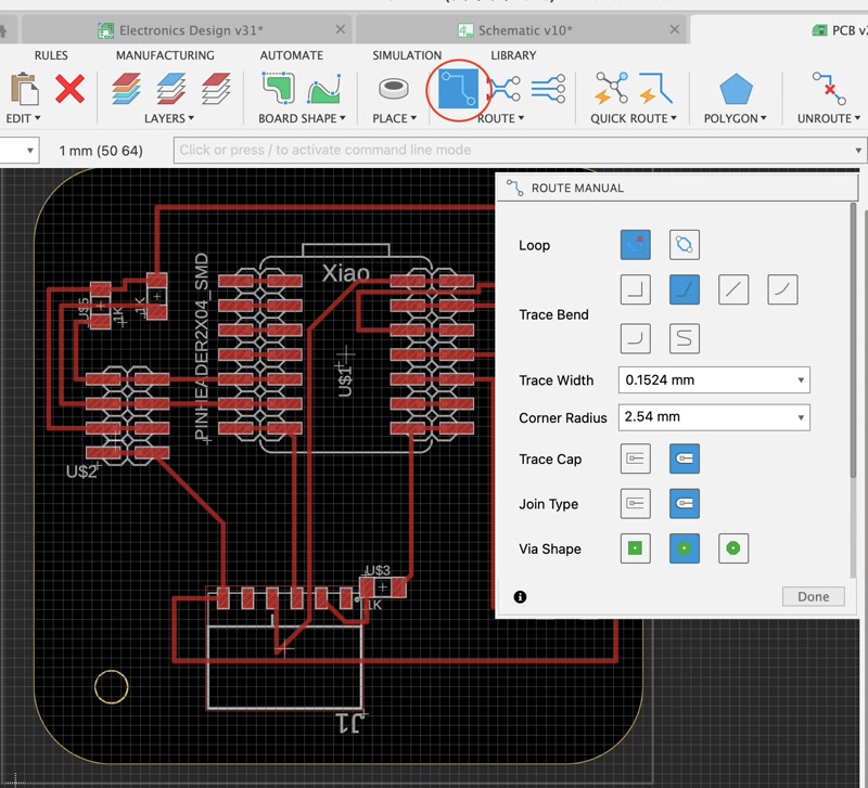
Arrange each component in the appropriate position, and create a path using the “route” command.
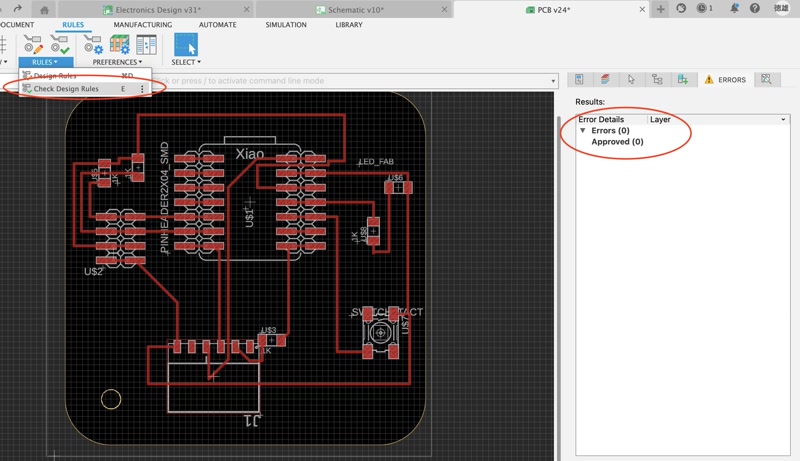
After creating the path, execute the DRC command to check for errors. Check the contents of the error messages, and make corrections until there are no errors.
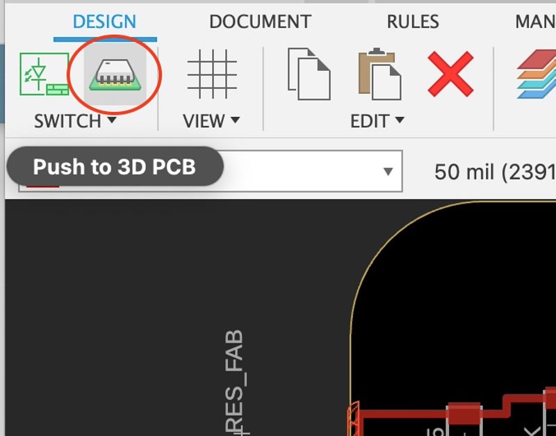
Push to 3D PCB
Select “Switch” > “Push to 3D PCB” from the menu to push the 3D data.
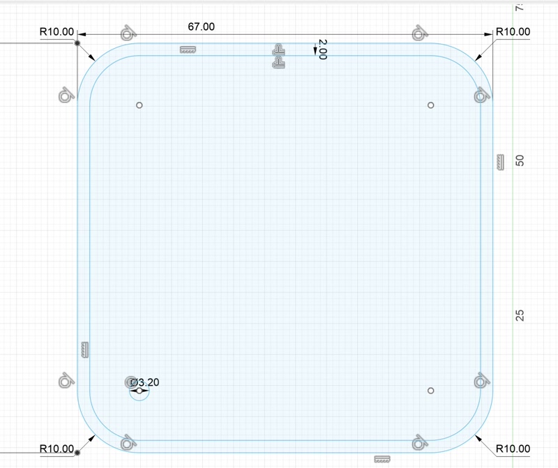
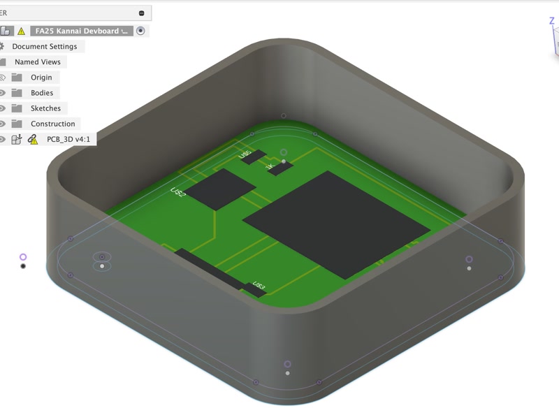
Design of enclosure
Right-click on “PCB_3D” in the data panel > Select “Insert into current design” to design the enclosure based on the PCB dimensions.
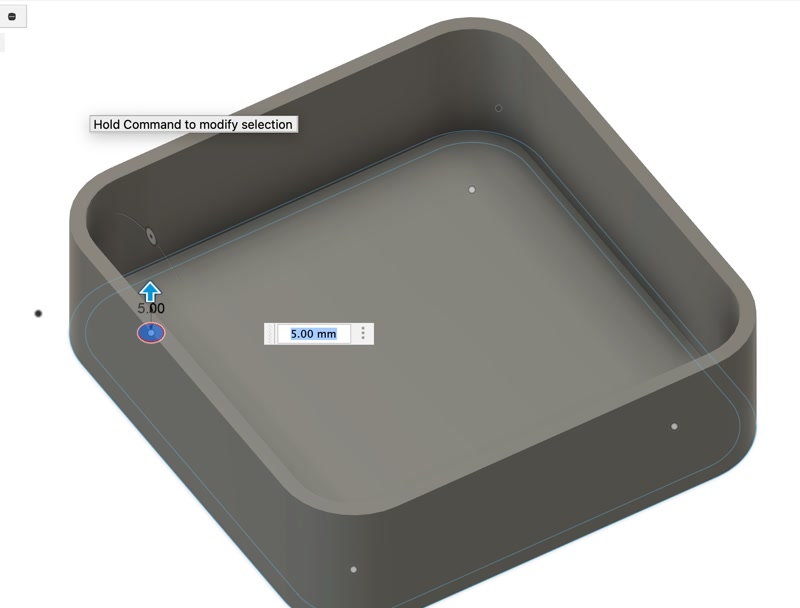
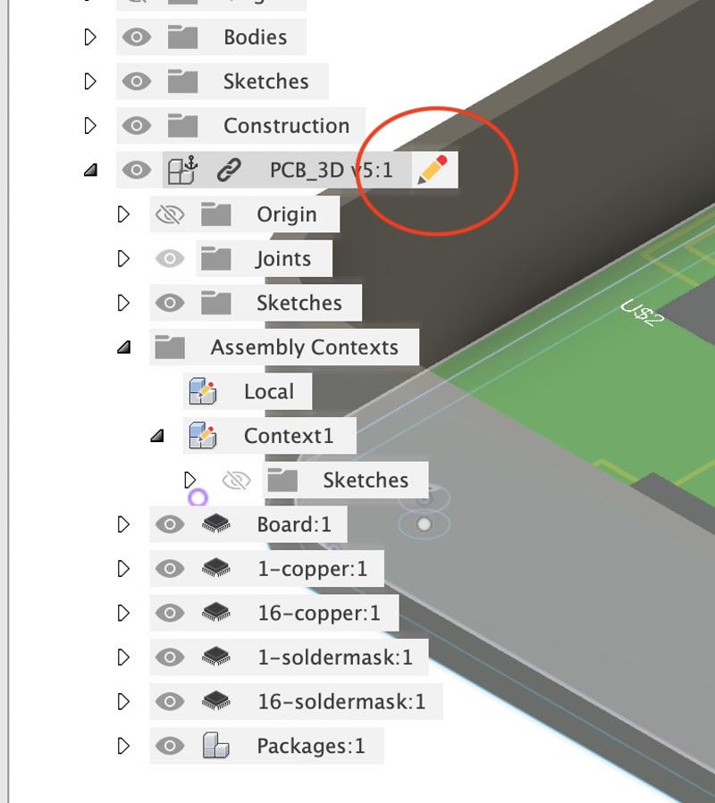
Update PCB outline (adjusted to match enclosure)
- Select the PCB_3D component and click the “pencil icon” to start in-place editing.
- Select PCB_3D > Outline Sketch to delete the sketch (a warning will appear, but don't worry).
- Go to the History panel at the bottom and apply a new sketch from “Edit Board”.
- Select a new sketch from the Enclosure and adjust the PCB outline to fit the enclosure.
Design file
The following are the design files for the development board and its case that were designed using the EDA tool this time.
Afterthoughts
I felt that Fusion was suited to designing products with electronic circuits because the design of the circuit board and the design of the casing are seamlessly connected.
Using the “route” command to create a path in the PCB layout was fun and challenging, like solving a maze.