6. Electronics Design
Group assignment:
- Use the test equipment in your lab to observe the operation of a microcontroller circuit board.
Group Assignment Highlights
In this group assignment, we explored several essential test equipment used in electronics labs to observe and analyze microcontroller circuit boards. The key tools we worked with include:
1. Multimeter
- Purpose: Measures voltage, current, resistance, and continuity in circuits.
- Key Features:
- Auto/manual range selection.
- Overload and low battery indication.
-
Used for troubleshooting circuit issues (e.g., checking voltage levels, resistor values).
-
Application:
- Measured voltage levels in the Arduino circuit.
- Checked resistance of components.
2. Oscilloscope
- Purpose: Visualizes electrical signals over time, helping in debugging and signal analysis.
- Key Features:
- 200MHz bandwidth for accurate signal capture.
- Supports multiple channels for comparing signals.
- Displays digital and analog waveforms.
- Application:
- Observed digital signals from the microcontroller.
- Verified PWM (Pulse Width Modulation) signals.
3. Function Generator
- Purpose: Generates test signals (sine, square, triangular, ramp waves) for circuit testing.
- Key Features:
- 25MHz bandwidth.
- Adjustable frequency and amplitude.
- Application:
- Generated square, sine, and ramp waves.
- Displayed waveforms on the oscilloscope for analysis.
4. DC Power Supply
- Purpose: Provides stable DC voltage to power circuits.
- Key Features:
- Programmable voltage/current settings
- Overload and short-circuit protection
- Multiple isolated outputs
- Application:
- Supplied power to the microcontroller board.
- Verified voltage output using a multimeter.
These tools are fundamental in electronics testing, allowing us to measure, visualize, and verify circuit behavior. The multimeter helps in basic checks, the oscilloscope provides detailed signal analysis, the function generator creates test signals, and the DC power supply provides stable power. Knowing how to use these instruments is crucial for debugging and optimizing microcontroller-based systems.
Here is the link to our group assignment.
Individual assignment:
-
Use an EDA tool to design a development board that uses parts from the inventory to interact and communicate with an embedded microcontroller.
Extra credit: - Try another design workflow. - Design a case for it.
For the group assignment, we learn how to use some test equipments available in our lab. Here is the link to the Group assignment.
Individual Assignment
1. XIAO RP2040
I started by exploring the XIAO RP2040 Pin diagram so that I can think about how I can use it for my custom PCB.
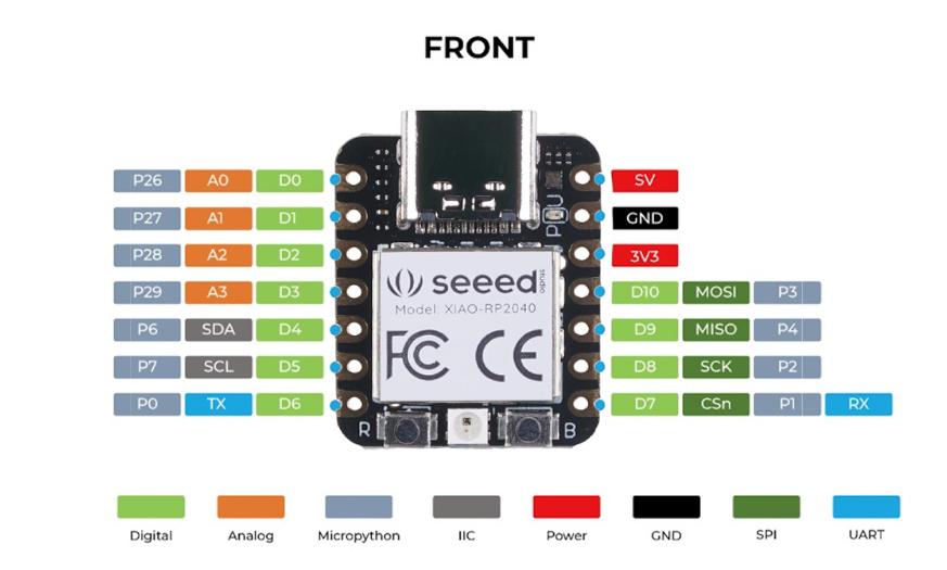
  *Specifications:*

  i. CPU: Dual-core ARM Cortex M0+ processor up to 133MHz

  ii. Flash Memory: 2MB

  iii. SRAM: 264KB

  iv. Digital I/O Pins: 11

  v. Analog I/O Pins: 4

  vi. PWM Pins: 11

  v. I2C interface: 1

  vi. SPI interface: 1

  vii. UART interface: 1

  viii. Power supply and downloading interface: Type-C

  ix. Power: 3.3V/5V DC

  x. Dimensions: 21×17.8×3.5mm
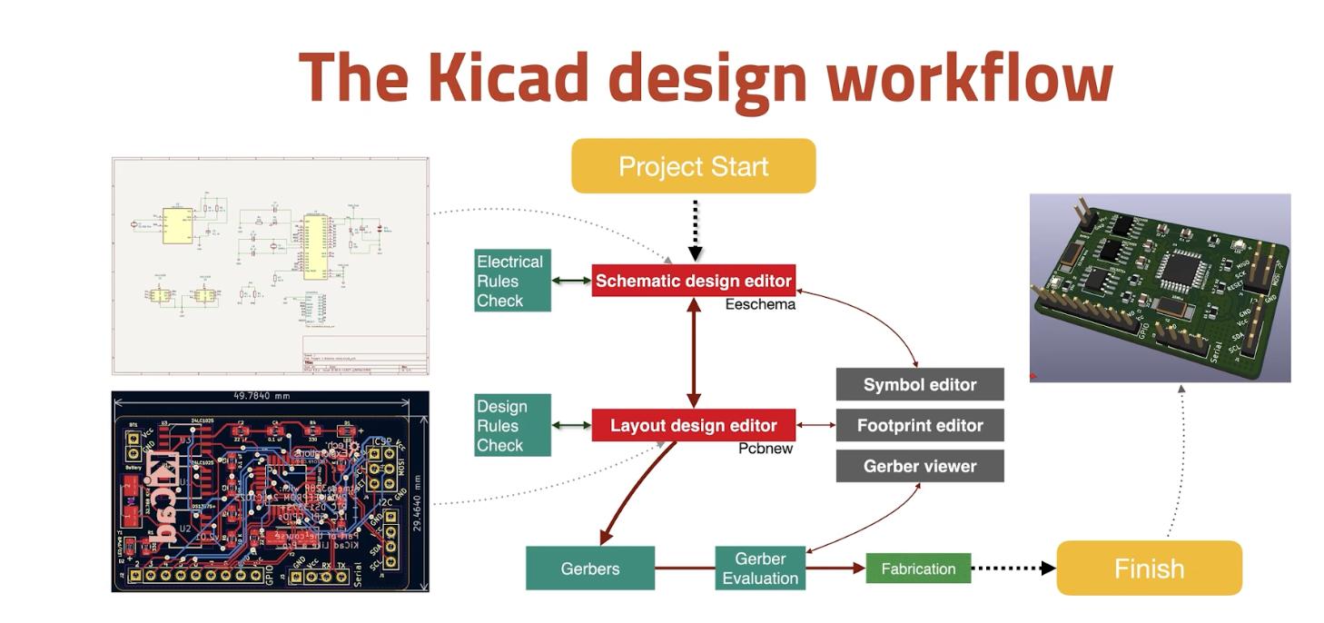
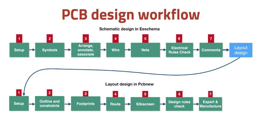
2. Kicad Design Workflow - I have included some images form PCB Designing course I had taken on Udemy few months ago. These are some pictures which are very helpful for me to understand the PCD designing workflow using Kicad.
-
This is the overall Kicad Design Workflow.
-
More elaborated Kicad Design Workflow.
-
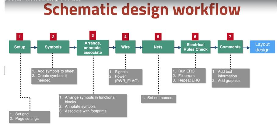
Breakdown of Schematic Design Workflow.
-
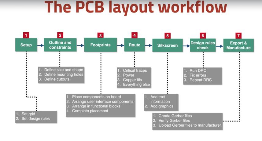
Breakdown of the PCB layout Workflow.
3. Designing a development board in Kicad Since I am already familiar with the kicad Desing Workflow, I don’t have to learn kicad from Basic.
-
I Downloaded Kicad from here.
-
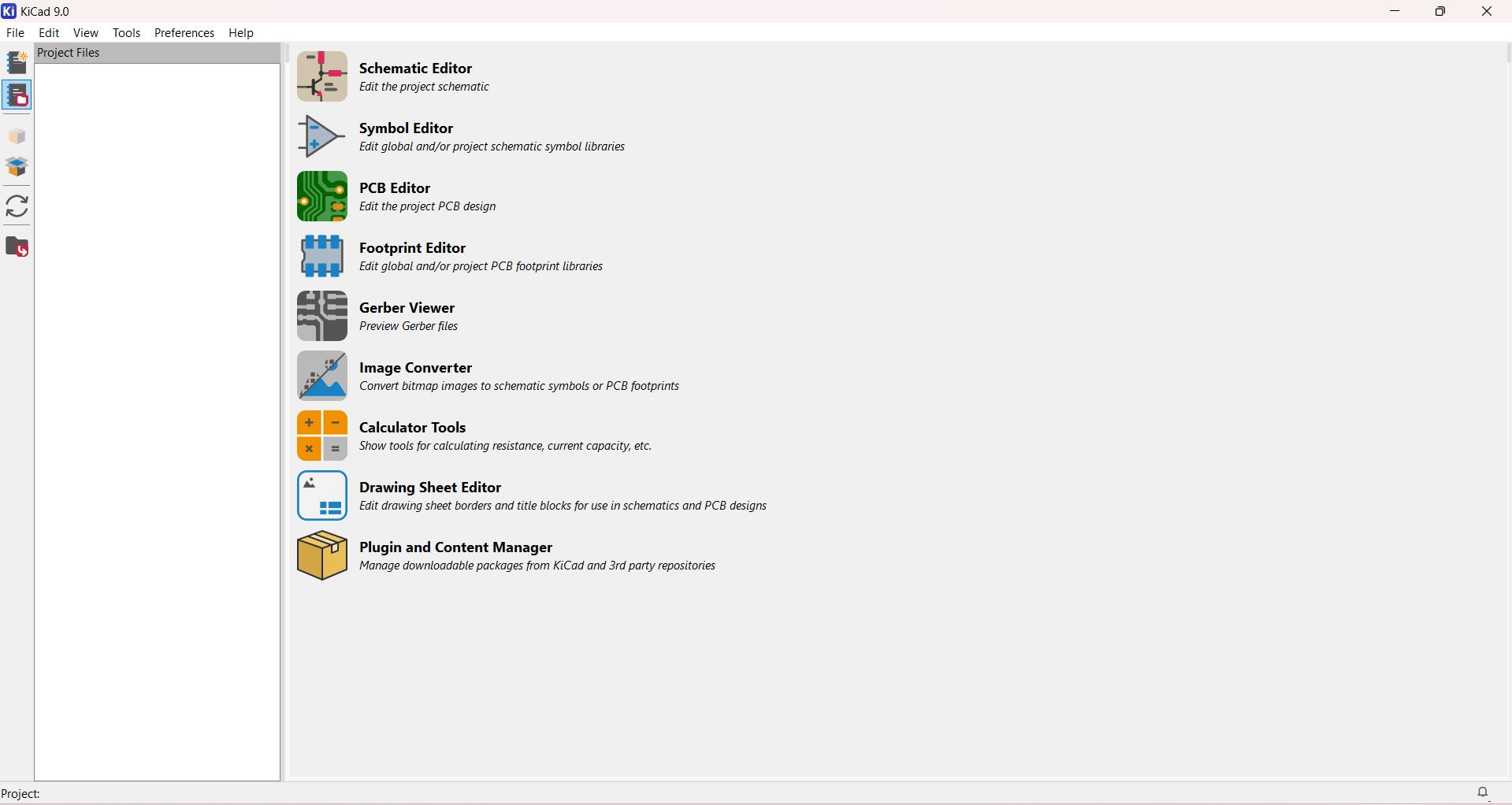
Open Kicad.
-
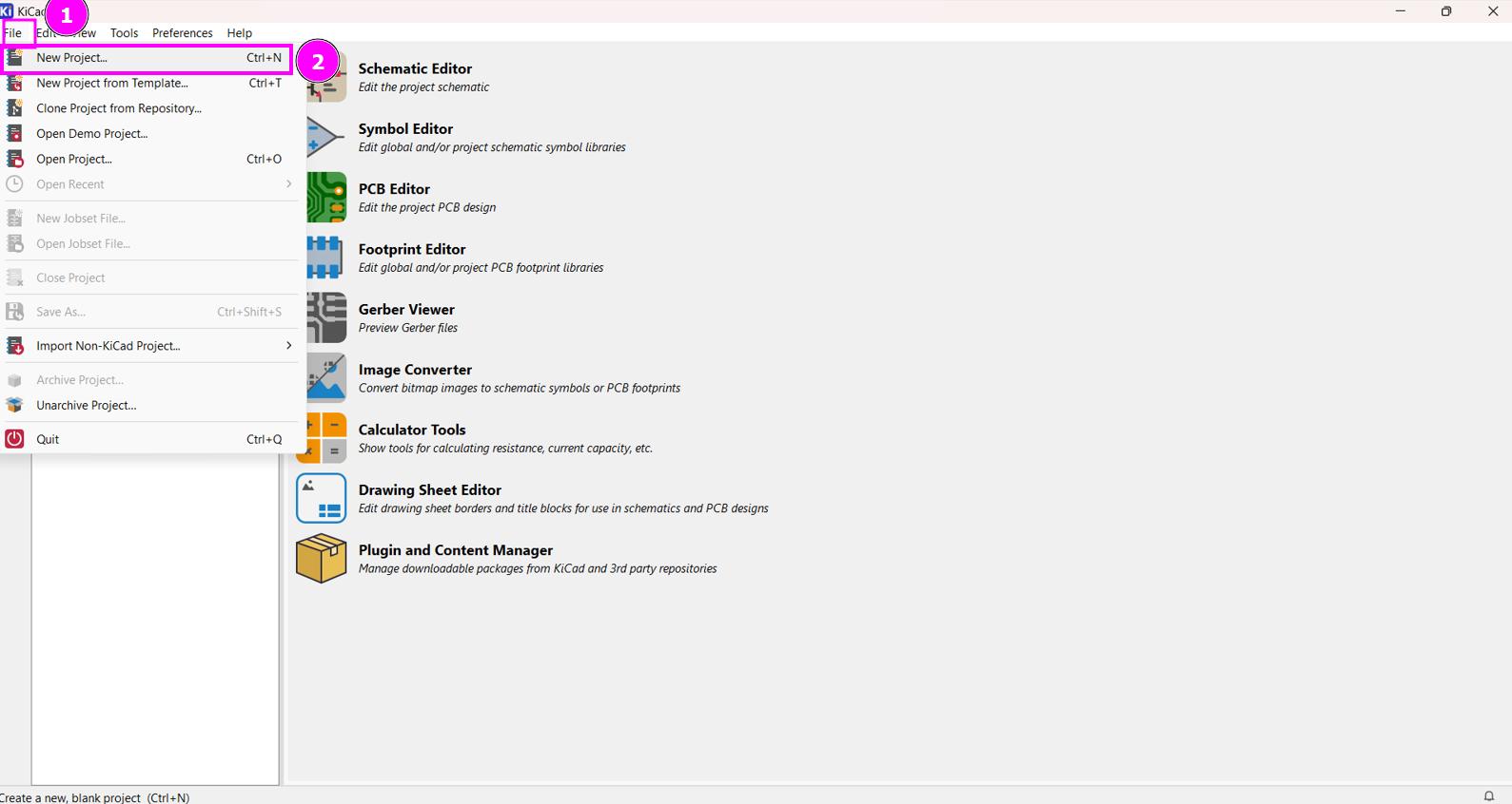
Create a new project.
-
Once you created your project, go to the Schematic Editor where you can build your circuit.
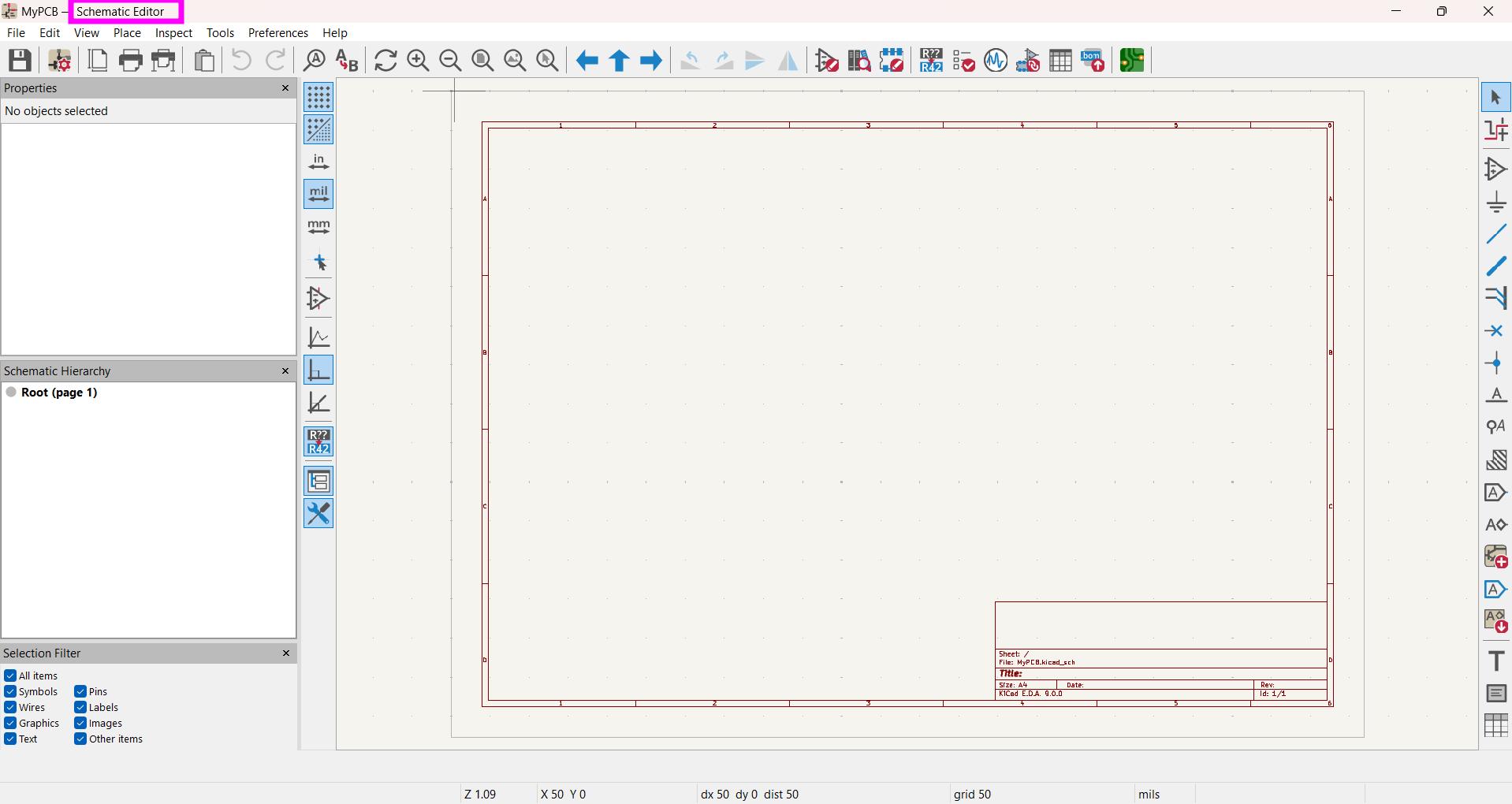
-
This is the interface of Schematic Editor.
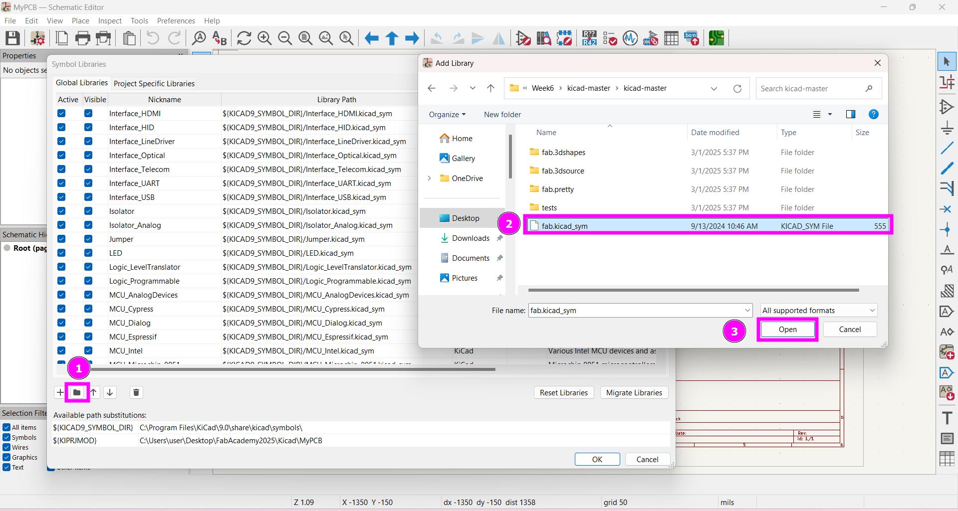
-
Download Fab Library for symbols and footprint form here.
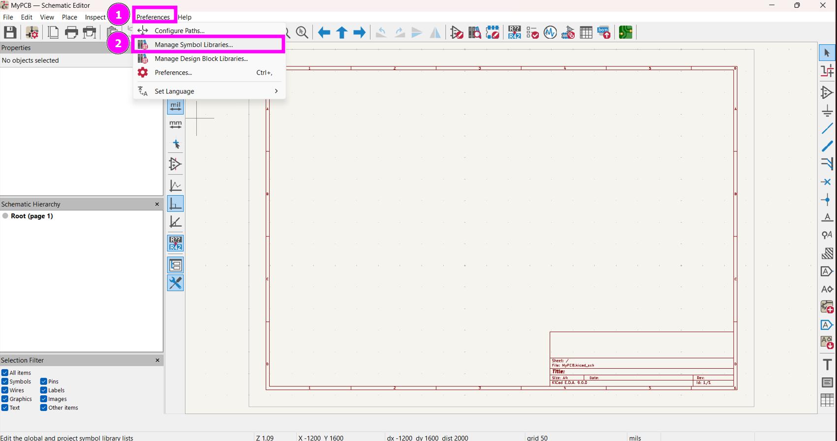
-
Click on Preferences*>>Manage Symbol Libraries** to add fab Libraries for symbol.
-
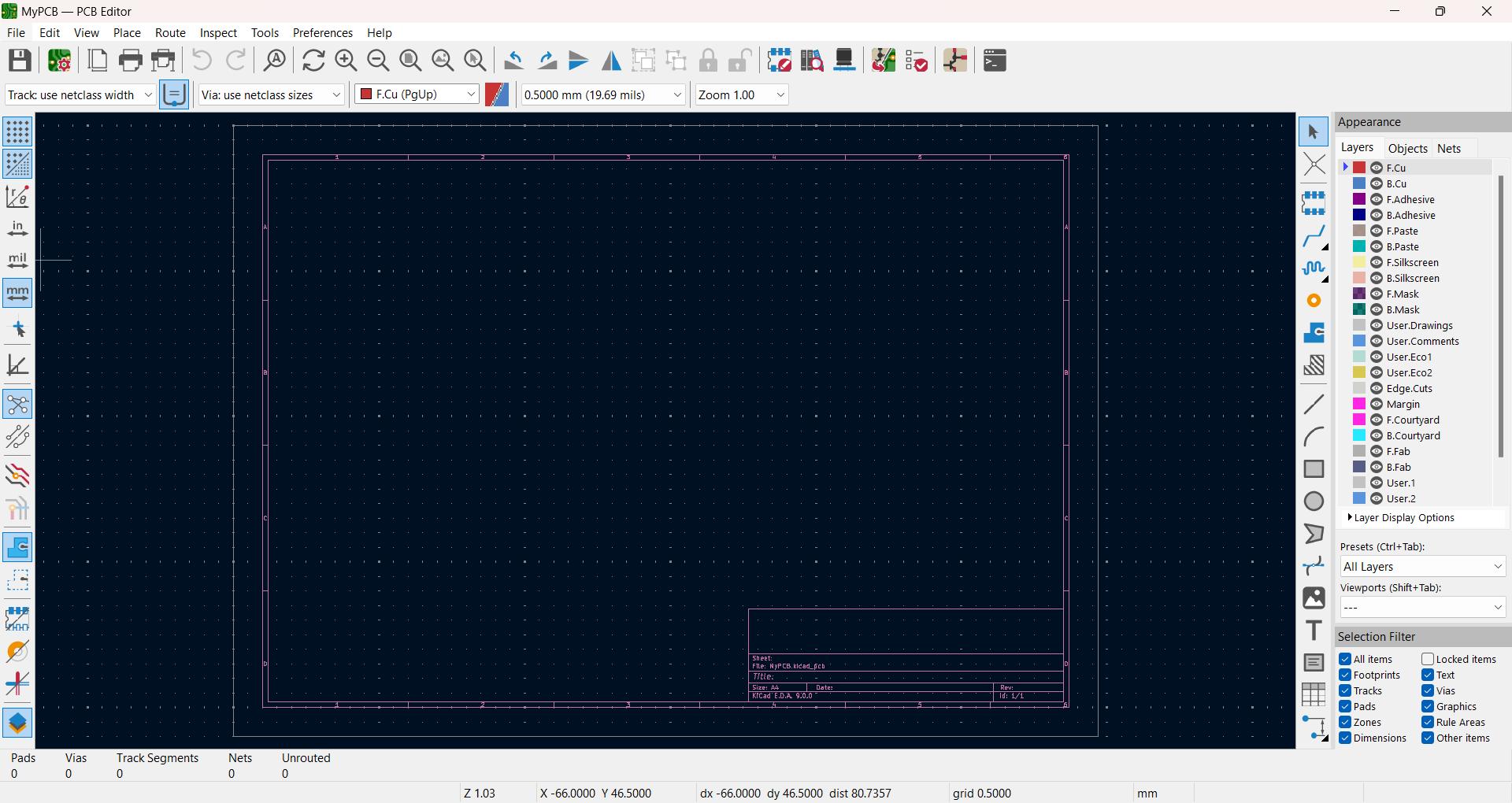
Now go to PCB Editor
-
This is the Interface of PCB Editor.
-
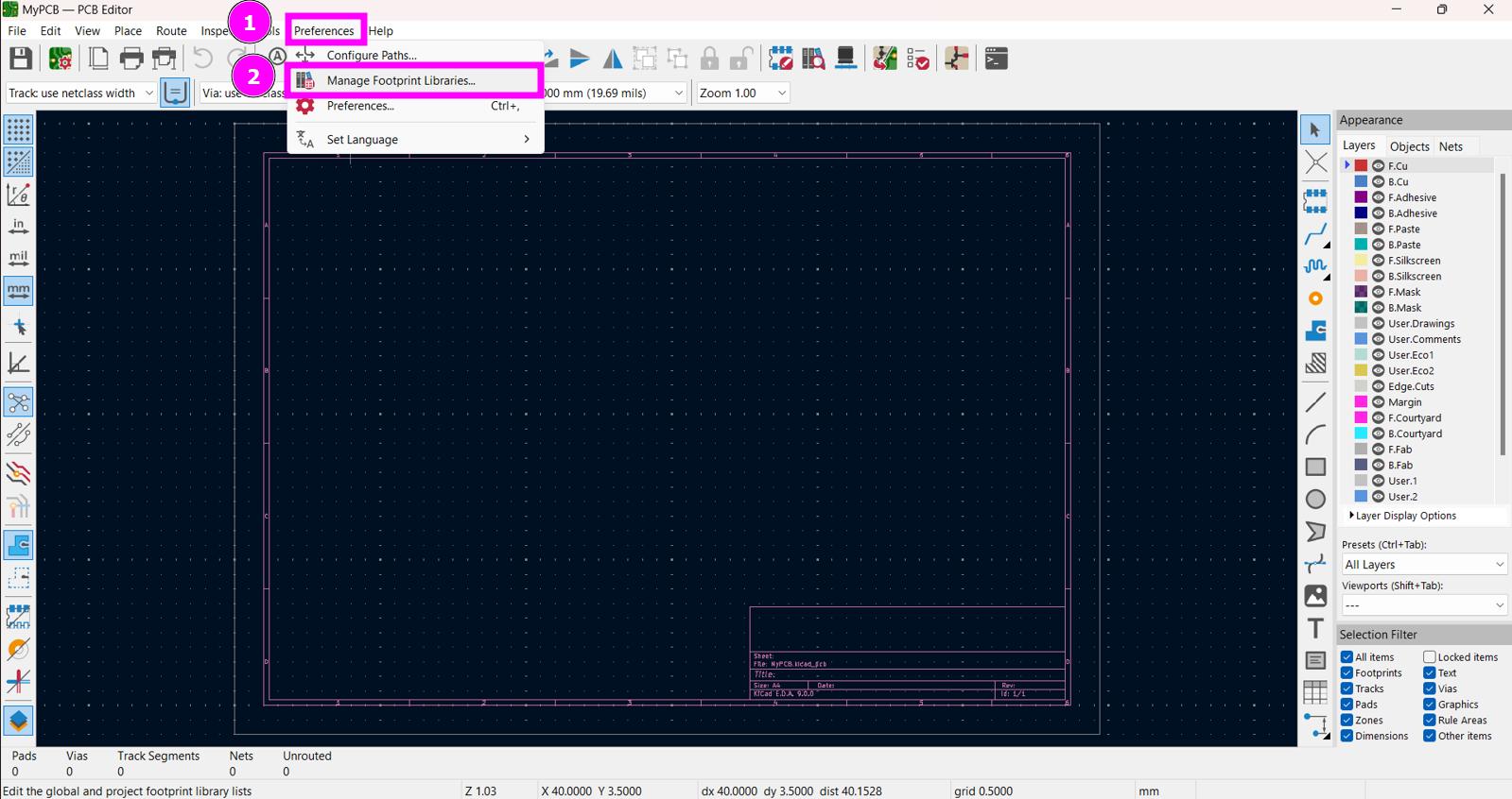
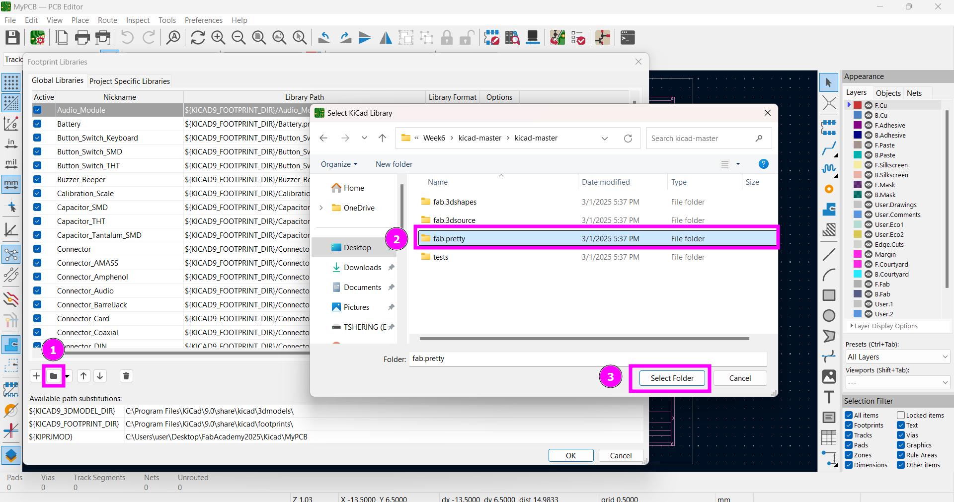
Go to the Preferences>>Manage Footprint Libraries to add fab footprint library
-
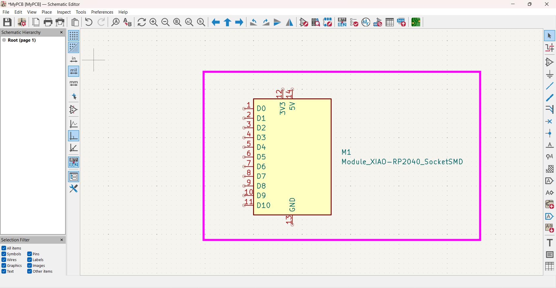
Now that I have added fab libraries for both symbol and Footprint, I will start with the schematic design for my PCB by adding symbol of RP2040 (SMD).
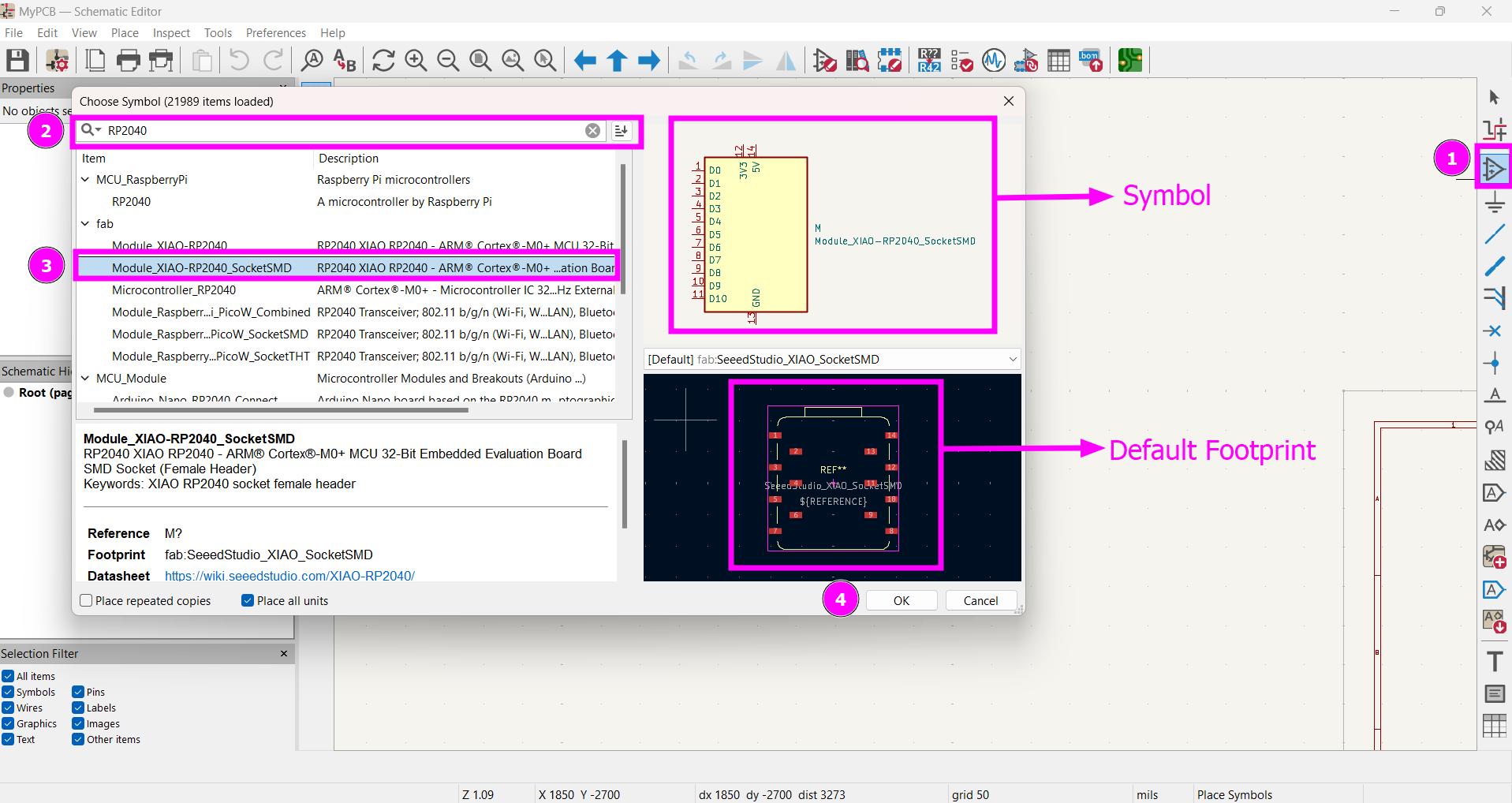
-
SMD Symbol for RP2040 added.
-
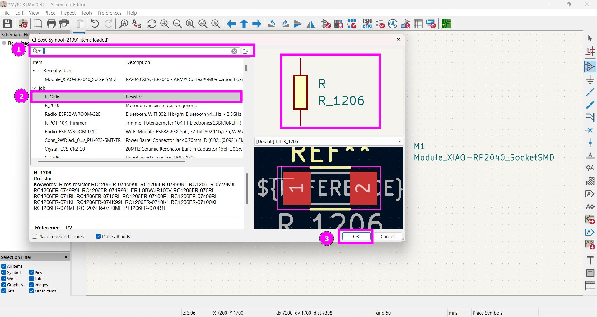
Add Resistor.
-
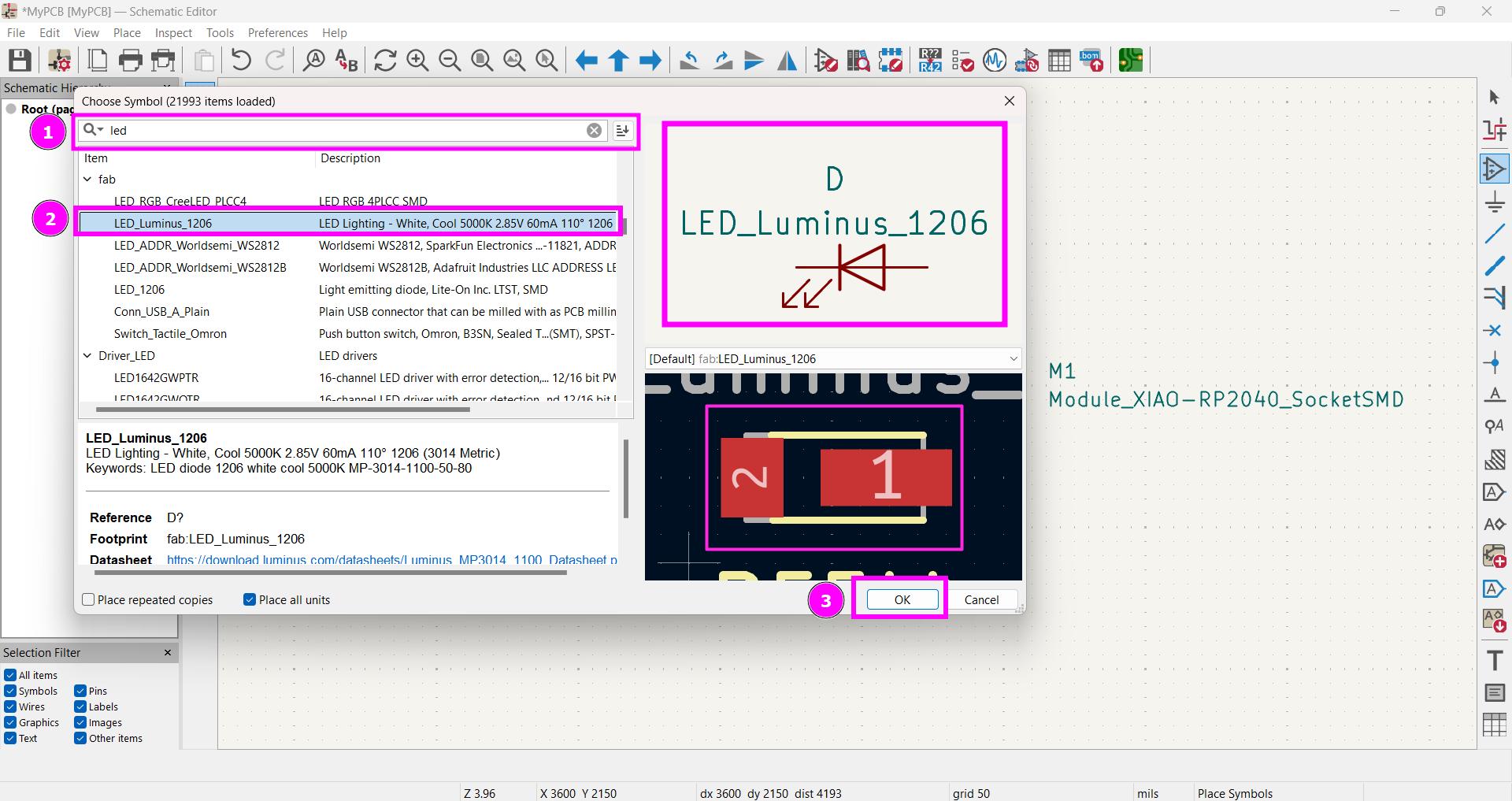
Add LED.
-
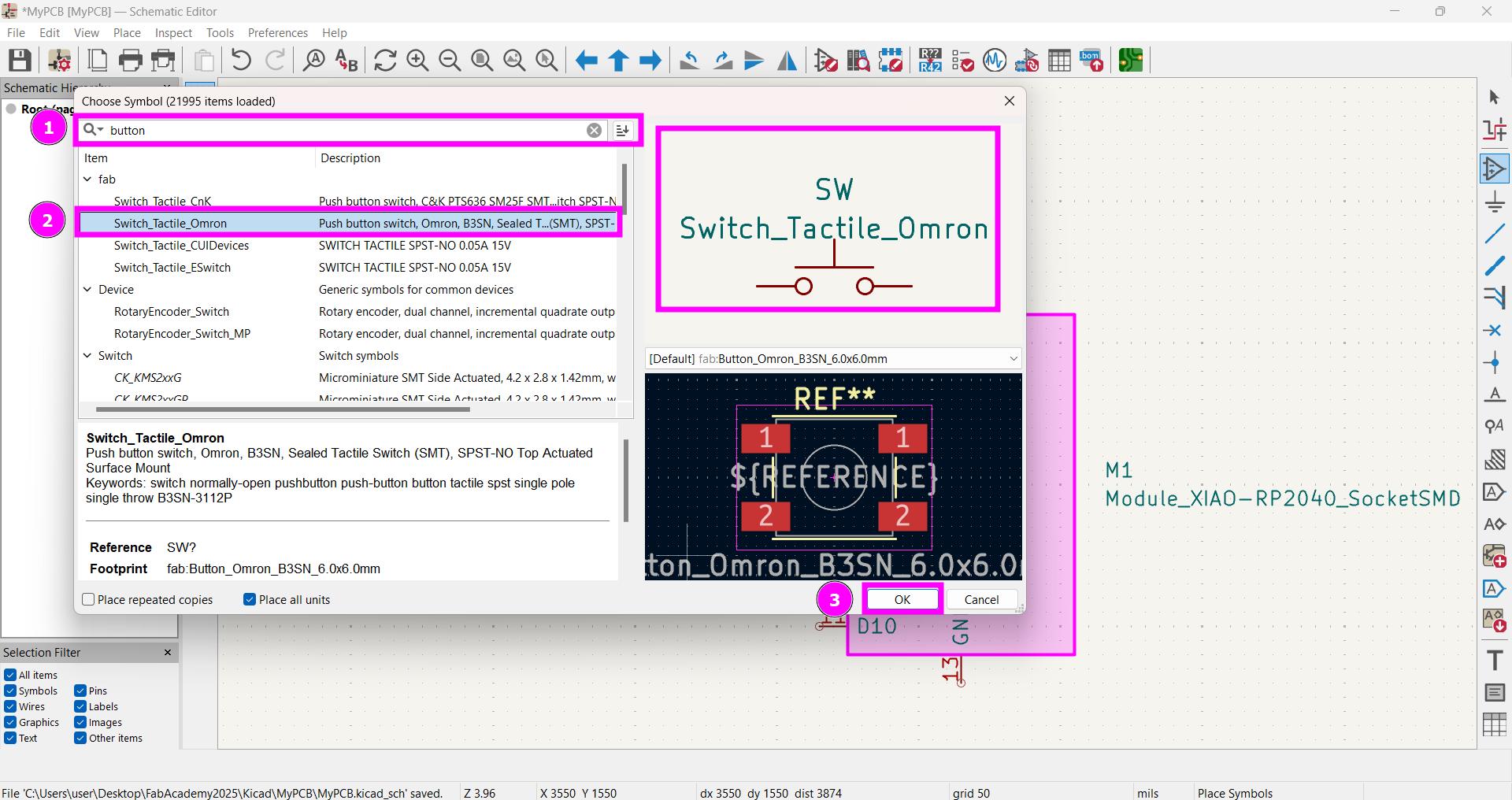
Add Switch.
-
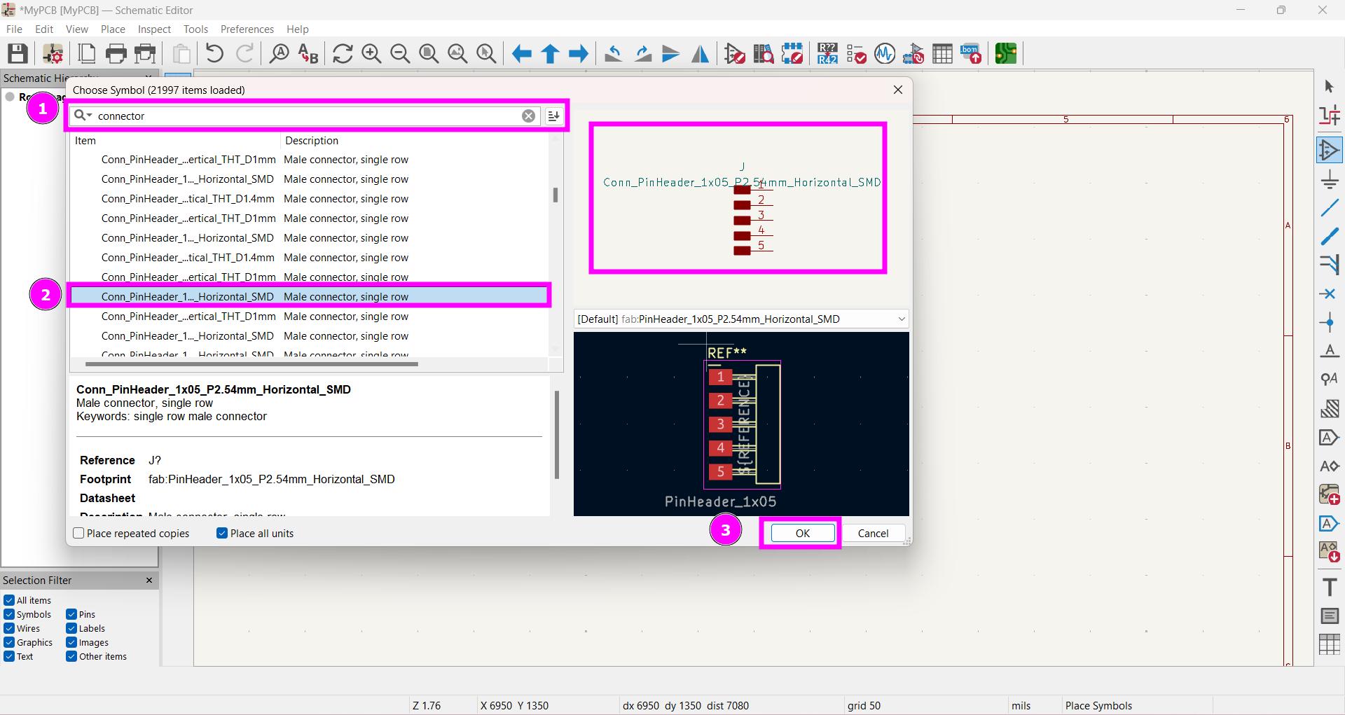
Add Connector.
-
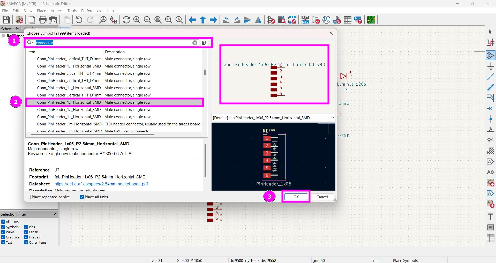
More connector.
-
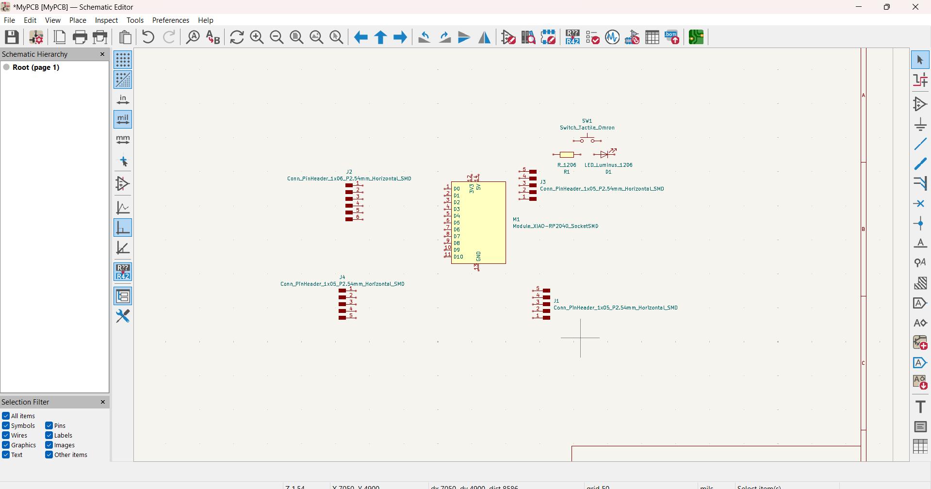
All the required components are added.
-
Wire the circuit using Net Label and run Electrical Rules Checker.
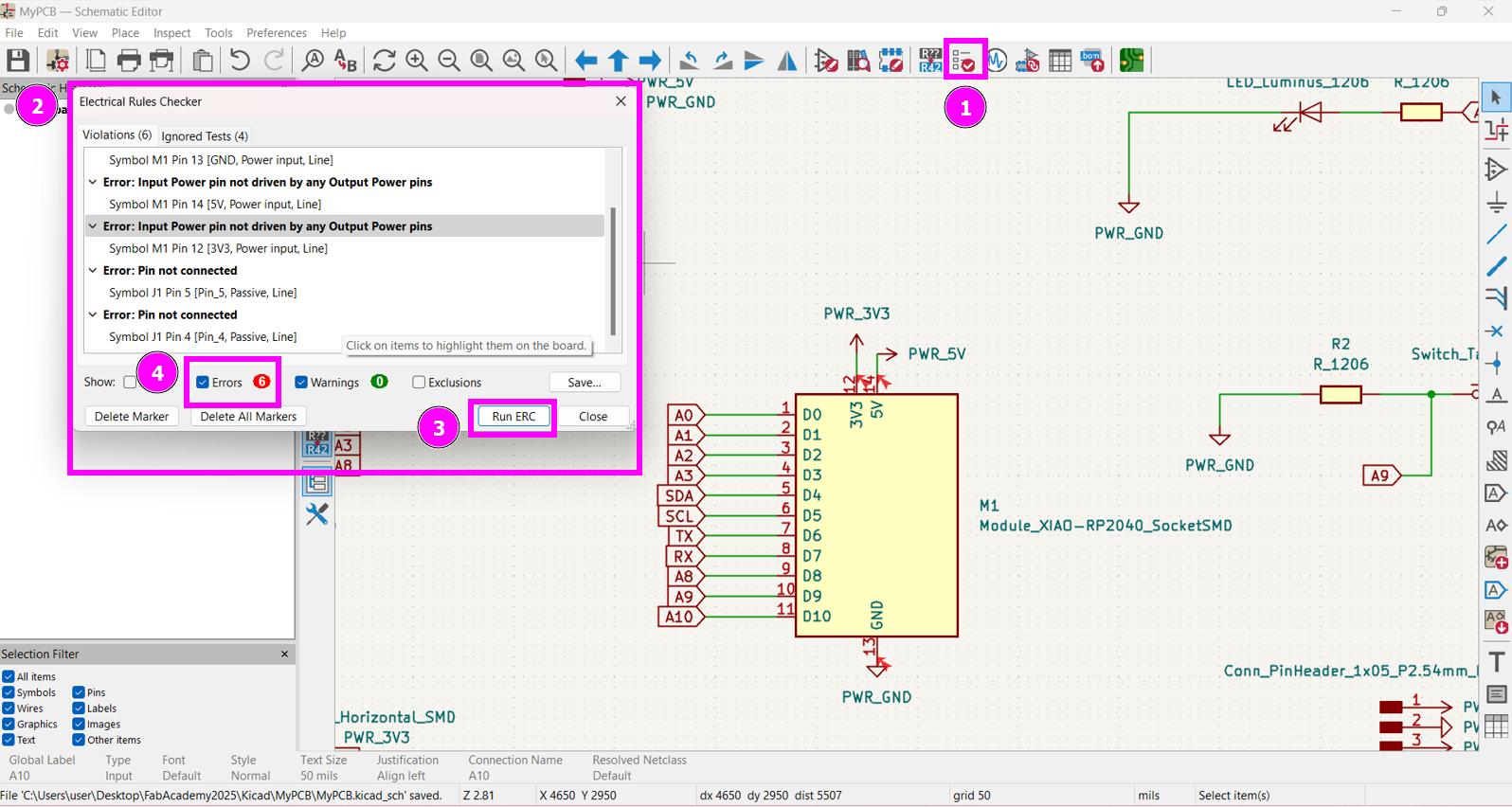 I encounter an error saying “Input Power pin not driven by Output Power pin”.
I fixed this by connecting a power flag to all the power line and ground.
I encounter an error saying “Input Power pin not driven by Output Power pin”.
I fixed this by connecting a power flag to all the power line and ground. -
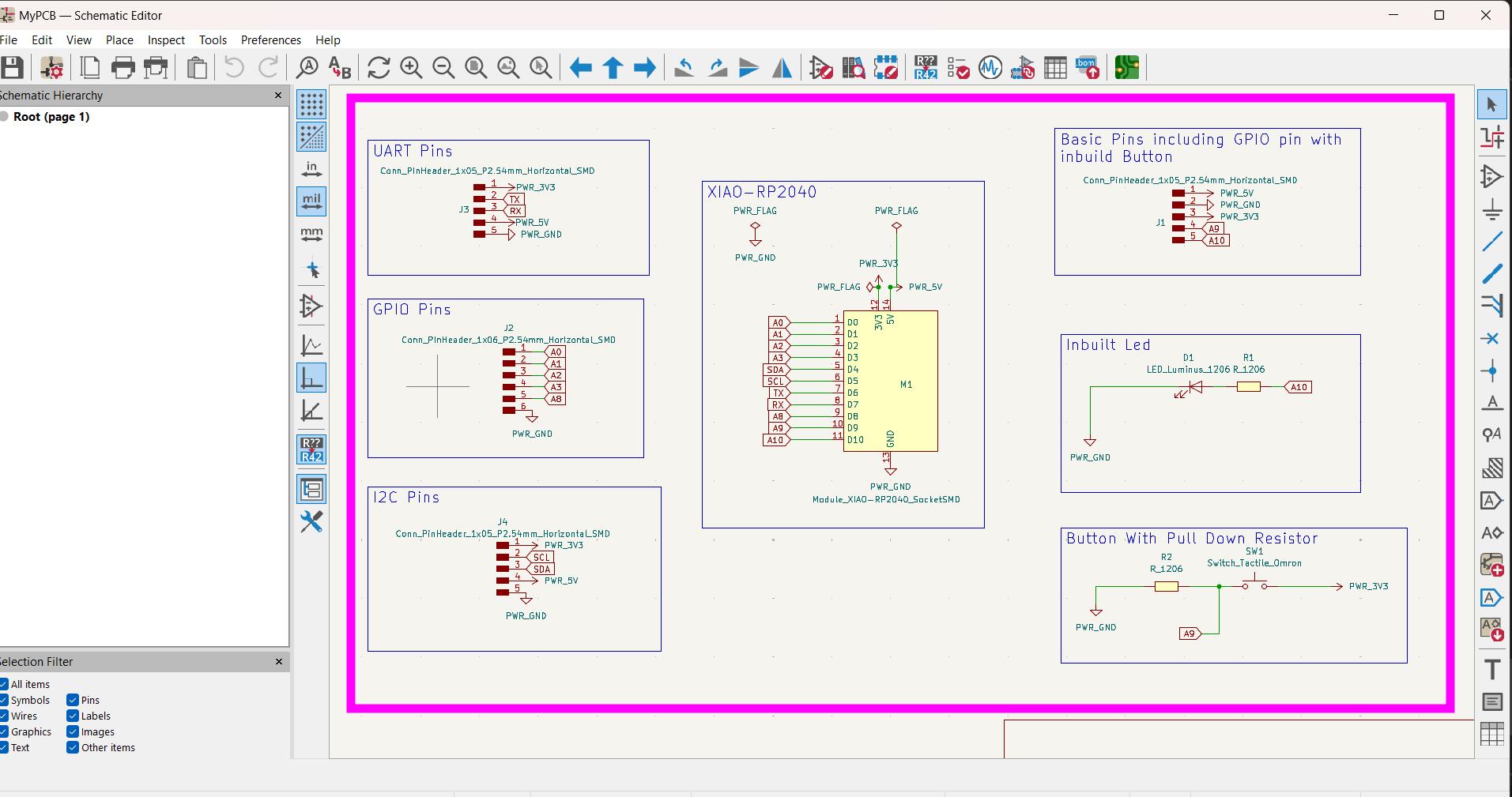
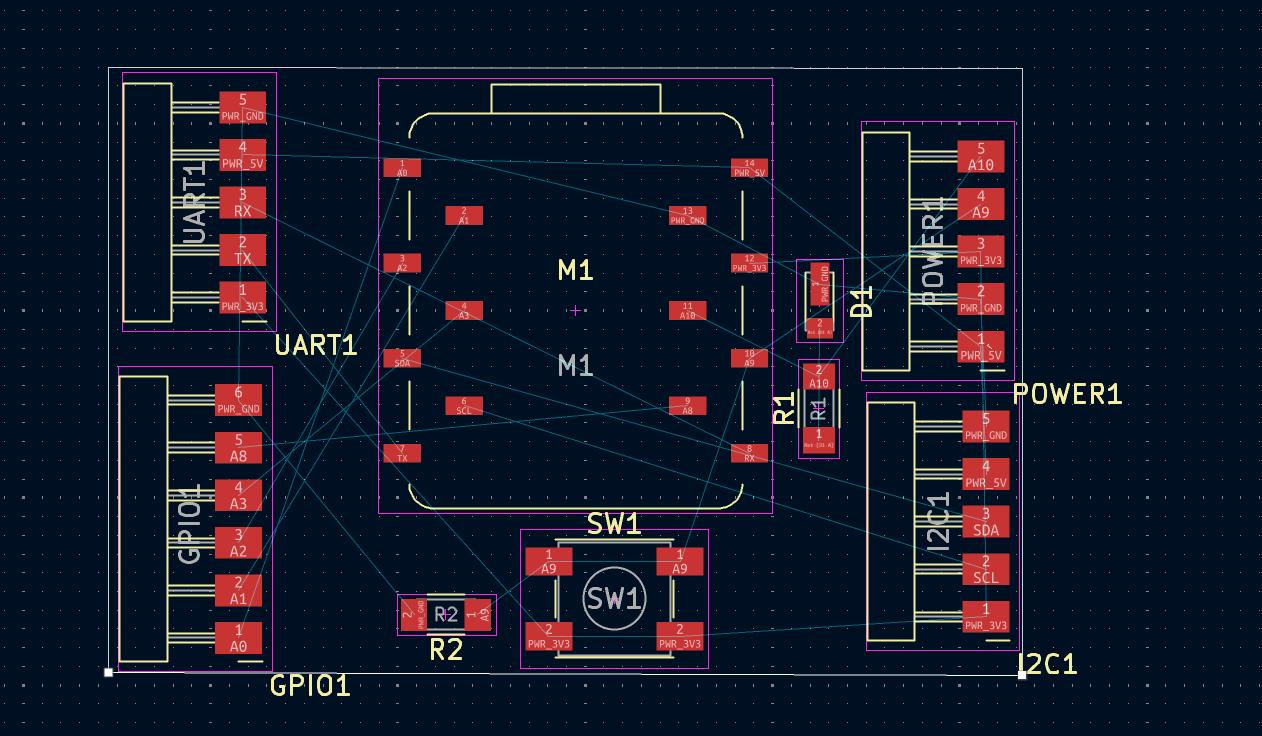
Arrange all the components and comment them with Box so that you can understand your circuit clearly.
-
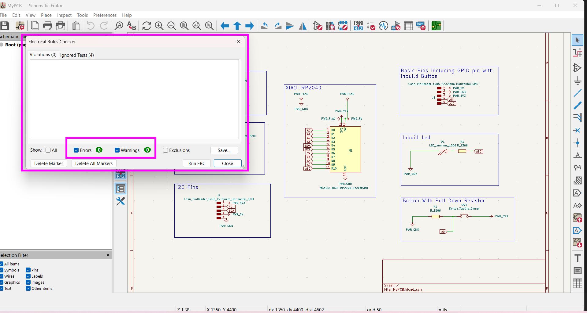
Run Electrical Rule Check once again to make sure you fix all the errors before going to PCB Editor.
-
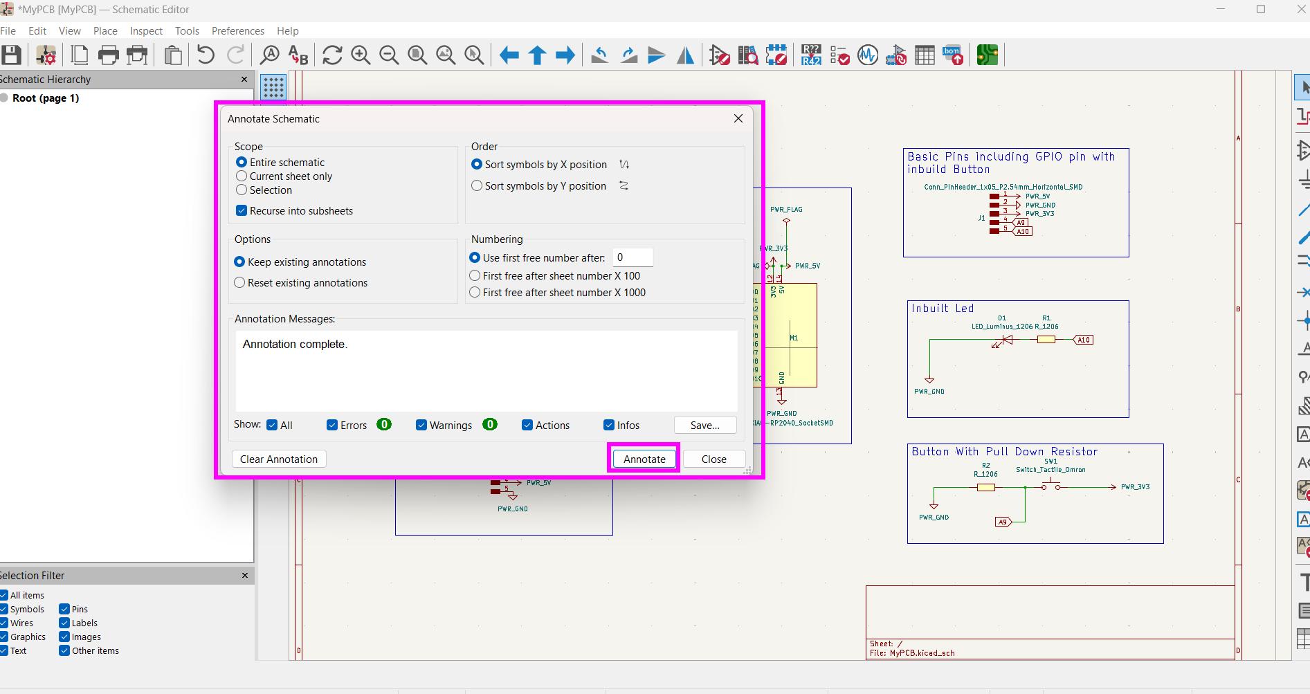
Also make sure to annotate your schematic.
-
Make sure you assigned right footprint required for your PCB according to the component you used.
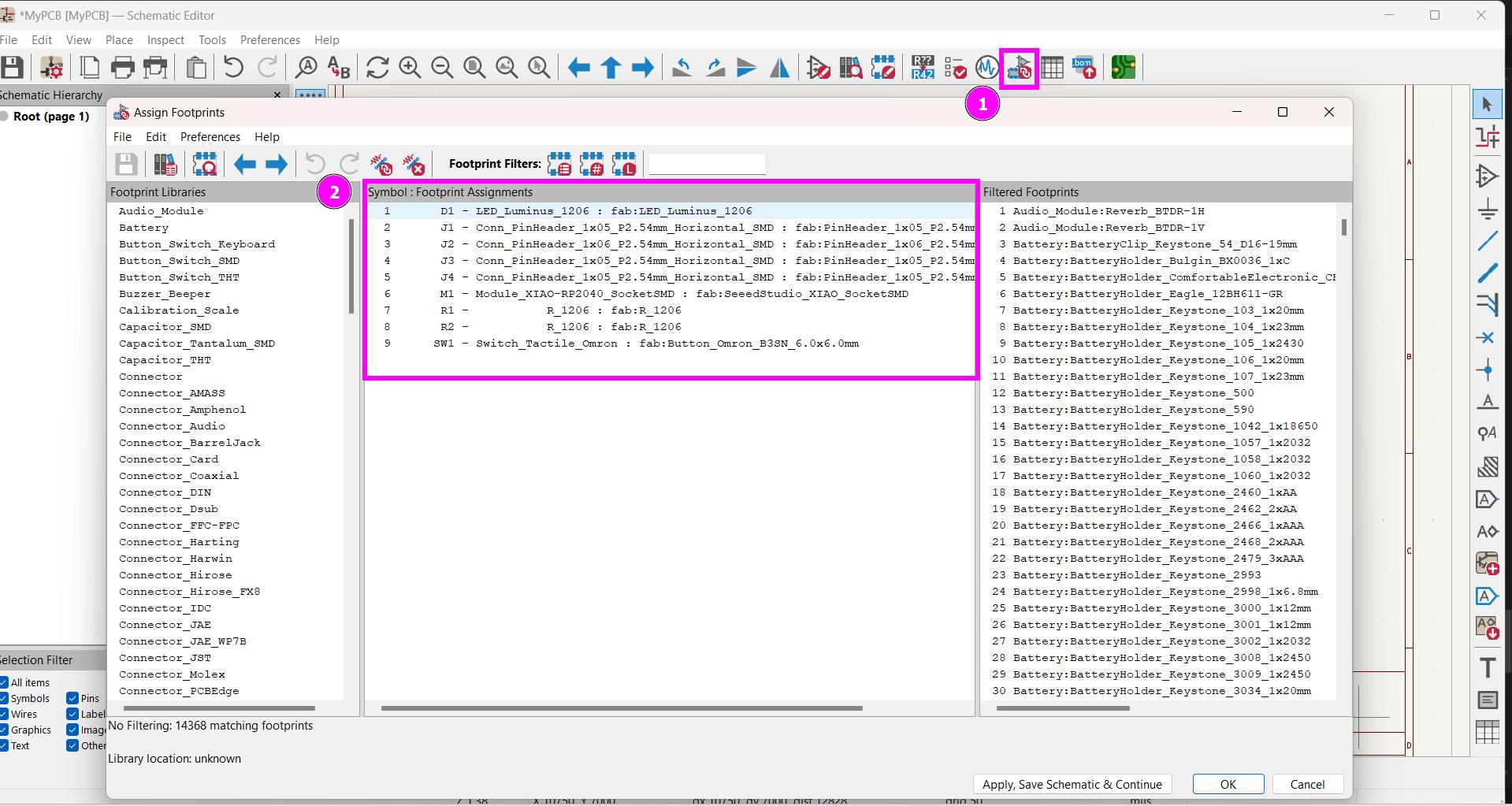
-
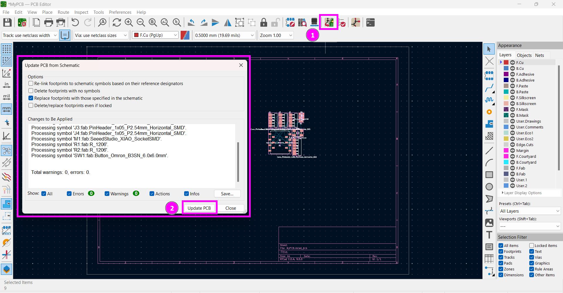
Jump to PCB Editor and update the footprint so that all the footprint will show up in PCB Editor.
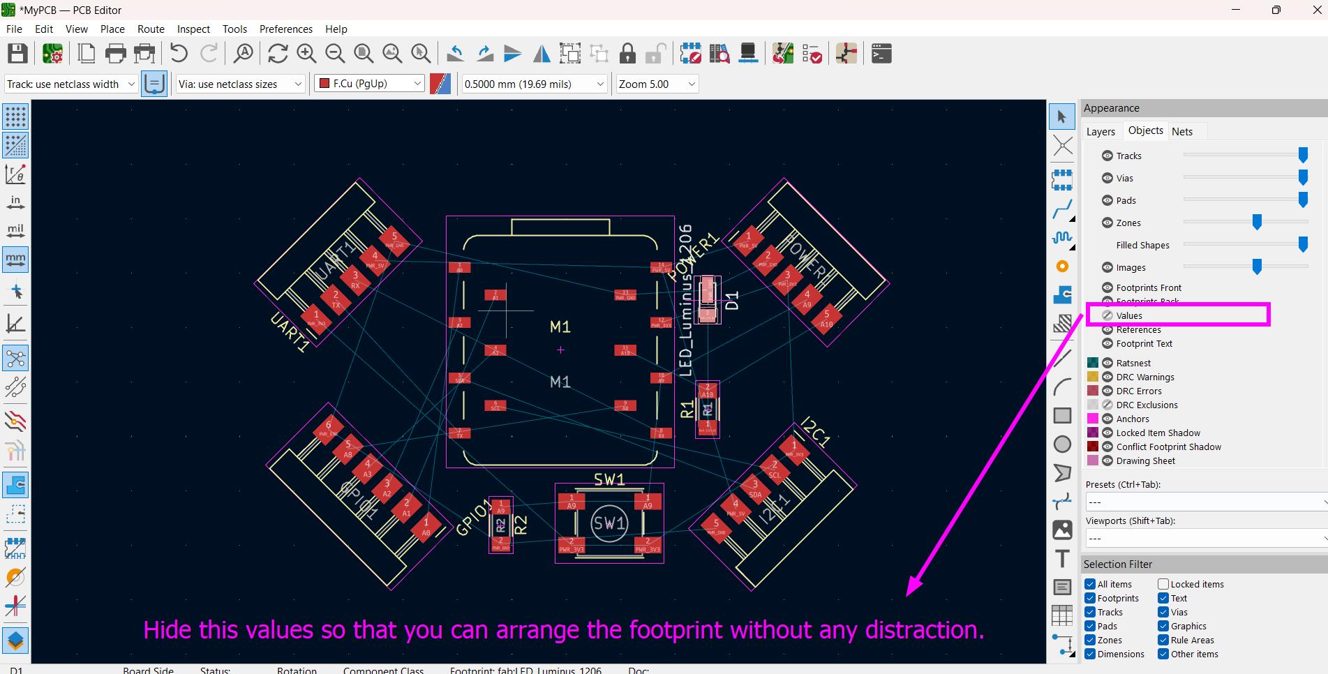
-
Arrange all the footprint carefully according to PCB design.
-
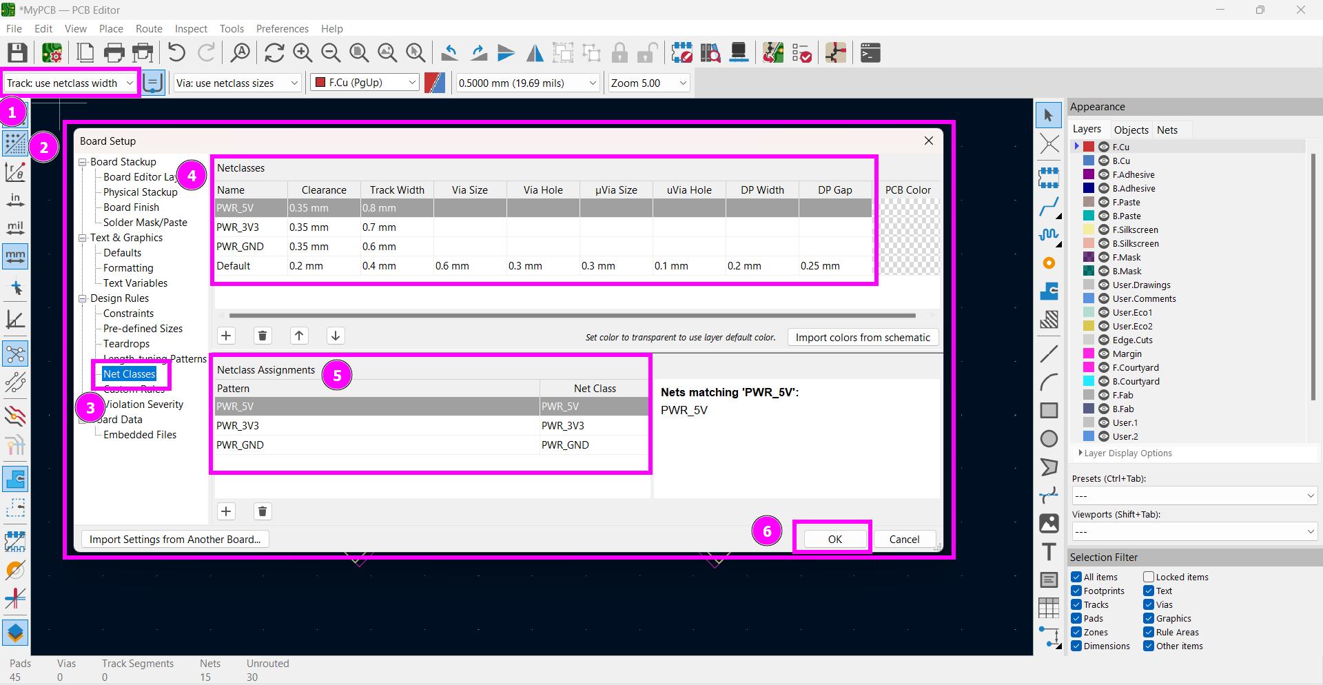
Now, define clearance and track width for each type of wire line used in your circuit ( you have to define via size and via hole if you are planning to design 2 or more layer PCB).
-
Create Edge Cute so that you can actually get an idea how to fit all your traces on the shape PCB you want to create. I preview my PCB and I does not look that good. I think I have to change it.
-
This one looks much better
-
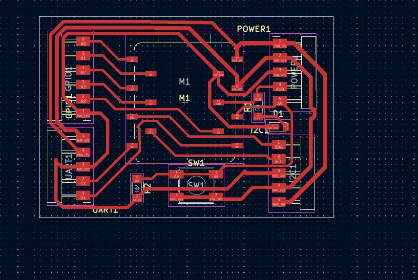
Route the Retsnest.
-
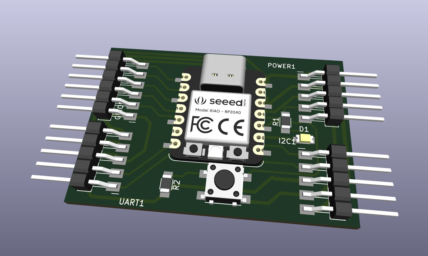
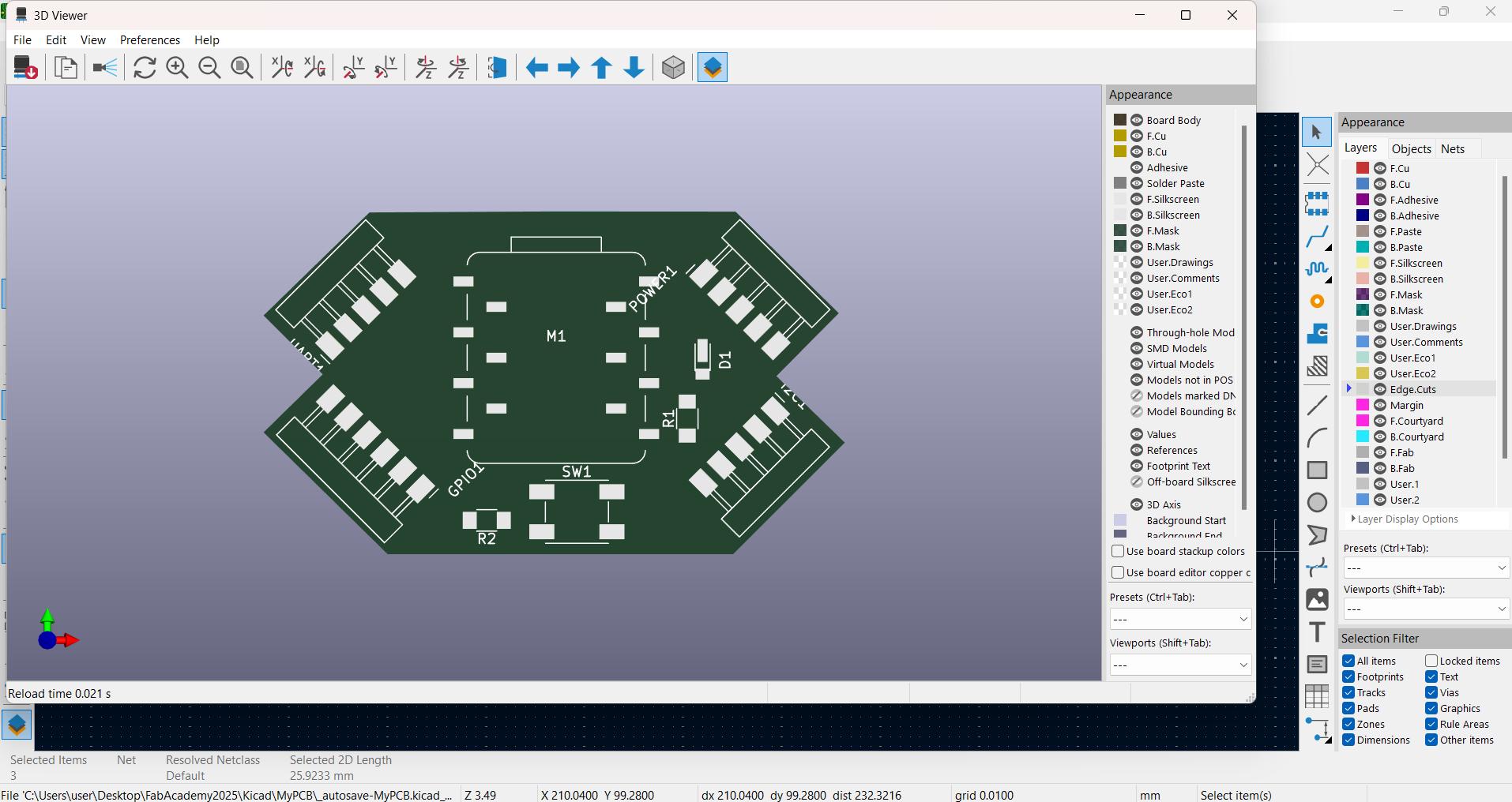
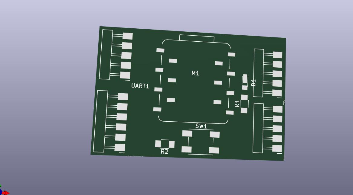
3D view of my PCB