Electronics Design
Learning outcomes
- Select and use software for circuit board design
- Demonstrate workflows used in circuit board design
Scheduling
As per usual, I started off my week by planning out my schedule.
Individual Assignment
For our individual assignment, we had to use a Electronic Design Automation (EDA) tool to create a development board that can communicate with an embedded microcontroller. I started off by researching EDA tools.
EDA Tools
Electronic Design Automation, or EDA, is a market segment consisting of software, hardware, and services with the collective goal of assisting in the definition, planning, design, implementation, verification, and subsequent manufacturing of semiconductor devices, or chips. - Synopsys
For this week, I’m going to stick to KiCad, which I’ll be talking about in a bit.
KiCad
“KiCad is a free and open-source electronics design automation (EDA) suite. It features schematic capture, integrated circuit simulation, printed circuit board (PCB) layout, 3D rendering, and plotting/data export to numerous formats. KiCad also includes a high-quality component library featuring thousands of symbols, footprints, and 3D models. KiCad has minimal system requirements and runs on Linux, Windows, and macOS.”
Here’s some more information from the actual KiCad website.
Tutorial
Before I start the design process, it’s important to understand what libraries and footprints are.
Libraries in PCB designing, libraries store schematic symbols and footprints, representing electrical components and their physical layout on the board. These collections make sure that your components are consistent and you don’t choose the wrong one by accident across projects.
Footprints Footprints represent the physical layout of electronic components, defining their actual size, shape, and pad placement for soldering. Accurately matching your footprints to your schematic symbols makes sure that your electrical connections are correct and your physical components are compatible during soldering.
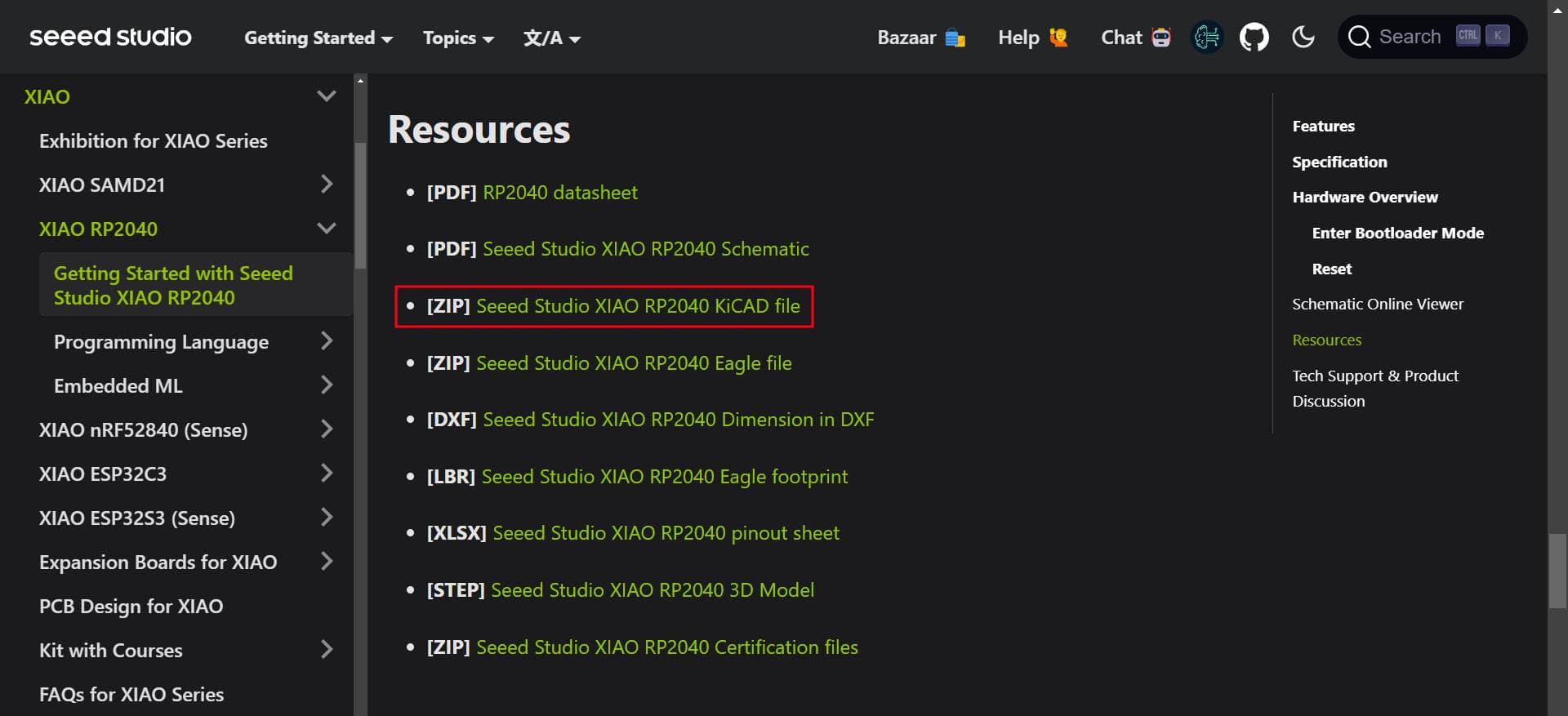
To start off this week, I installed a Seeeduino XIAO library for KiCad. I followed this tutorial, and you can find the official list of Seeeduino XIAO 2040 libraries here.
I downloaded the KiCad library file, and then I uploaded it to my KiCad libraries.
I found this tutorial series really useful throughout the week.
Information
| Name | Shortcut | Symbol Location | Function | Symbol |
|---|---|---|---|---|
| Select item | S | Schematic Editor | Selects an item in the schematic editor | |
| Add a symbol | A | Schematic Editor | Adds a new component to the schematic | |
| Add a power symbol | P | Schematic Editor | Adds a power symbol to the schematic | |
| Add a wire | W | Schematic Editor | Adds a wire for electrical connection | |
| Add a no-connection flag | Q | Schematic Editor | Adds a no-connection flag to indicate no electrical connection | |
| Add a junction | J | Schematic Editor | Adds a junction where two wires meet | |
| Add a global label | CTRL+L | Schematic Editor | Adds a global label to identify a net or signal | |
| Plot | N/A | Schematic Editor | Plots the schematic into a file format | |
| Schematic setup | N/A | Schematic Editor | Sets up the schematic properties | |
| Electrical Rules Checker | N/A | Schematic Editor | Checks the schematic for any electrical rule violations |
The Design Process
My Microcontroller
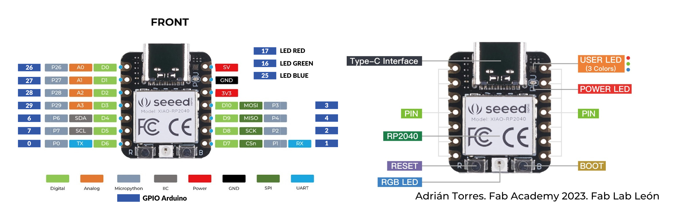
For this weeks design process, I decided to go back to the SEEED STUDIO XIAO RP2040 since it has a lot of different features and the ESP32 WROOM32D wasn’t really getting anywhere for me 😭.
Here’s the PINOUT diagram for the SEEED STUDIO XIAO RP2040, which is what I used as my main reference for this week (thanks Adrian 🙏).
Specifications
| Item | Value |
|---|---|
| CPU | Dual-core ARM Cortex M0+ processor up to 133MHz |
| Flash Memory | 2MB |
| SRAM | 264KB |
| Digital I/O Pins | 11 |
| Analog I/O Pins | 4 |
| PWM Pins | 11 |
| I2C interface | 1 |
| SPI interface | 1 |
| UART interface | 1 |
| Power supply and downloading interface | Type-C |
| Power | 3.3V/5V DC |
| Dimensions | 20×17.5×3.5mm |
The Schematic Layout
I’m sure everyone is pretty familiar with KiCad by now, as well as how the UI works, so I’ll be doing a bit less details for this weeks documentation. The general process is the same as the Embedded programming week, which you can find here, or you could check out the official KiCad page.
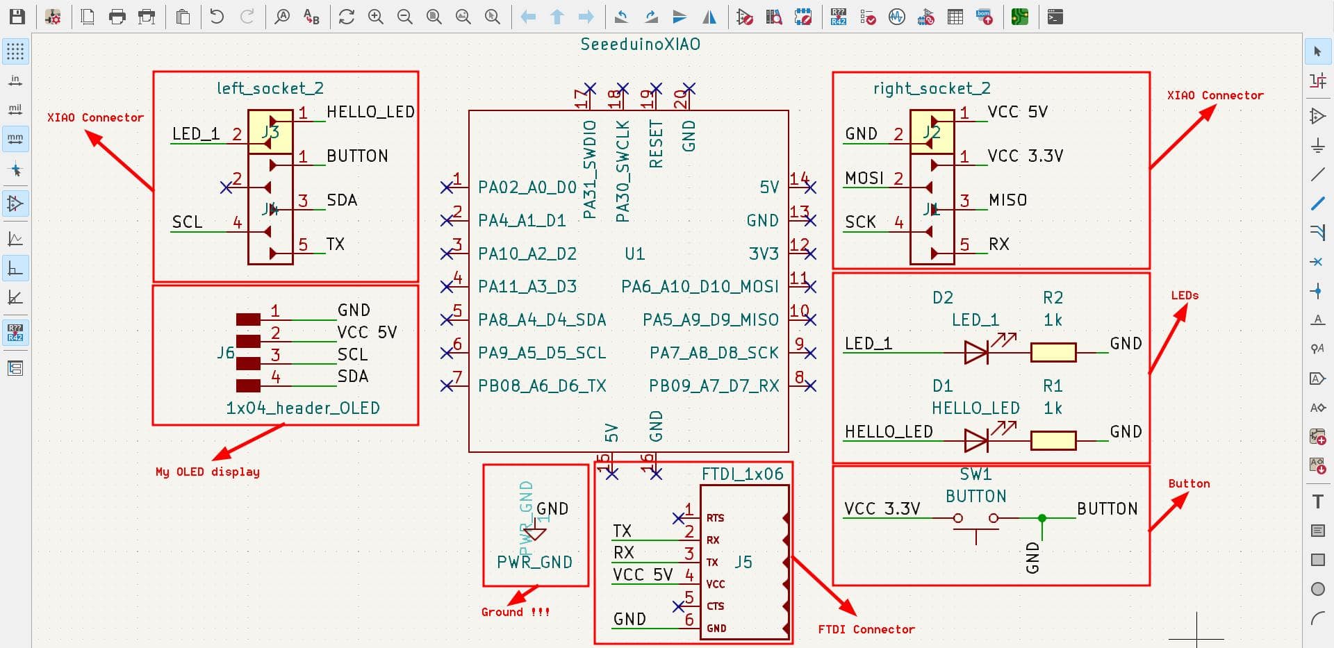
If you followed the KiCad tutorial from earlier, you should have all the libraries downloaded and ready. I used the QuenTorres board’s documentation as a reference, as well as random resources online such as component PINOUT diagrams. After connecting everything, this is the schematic that I got.
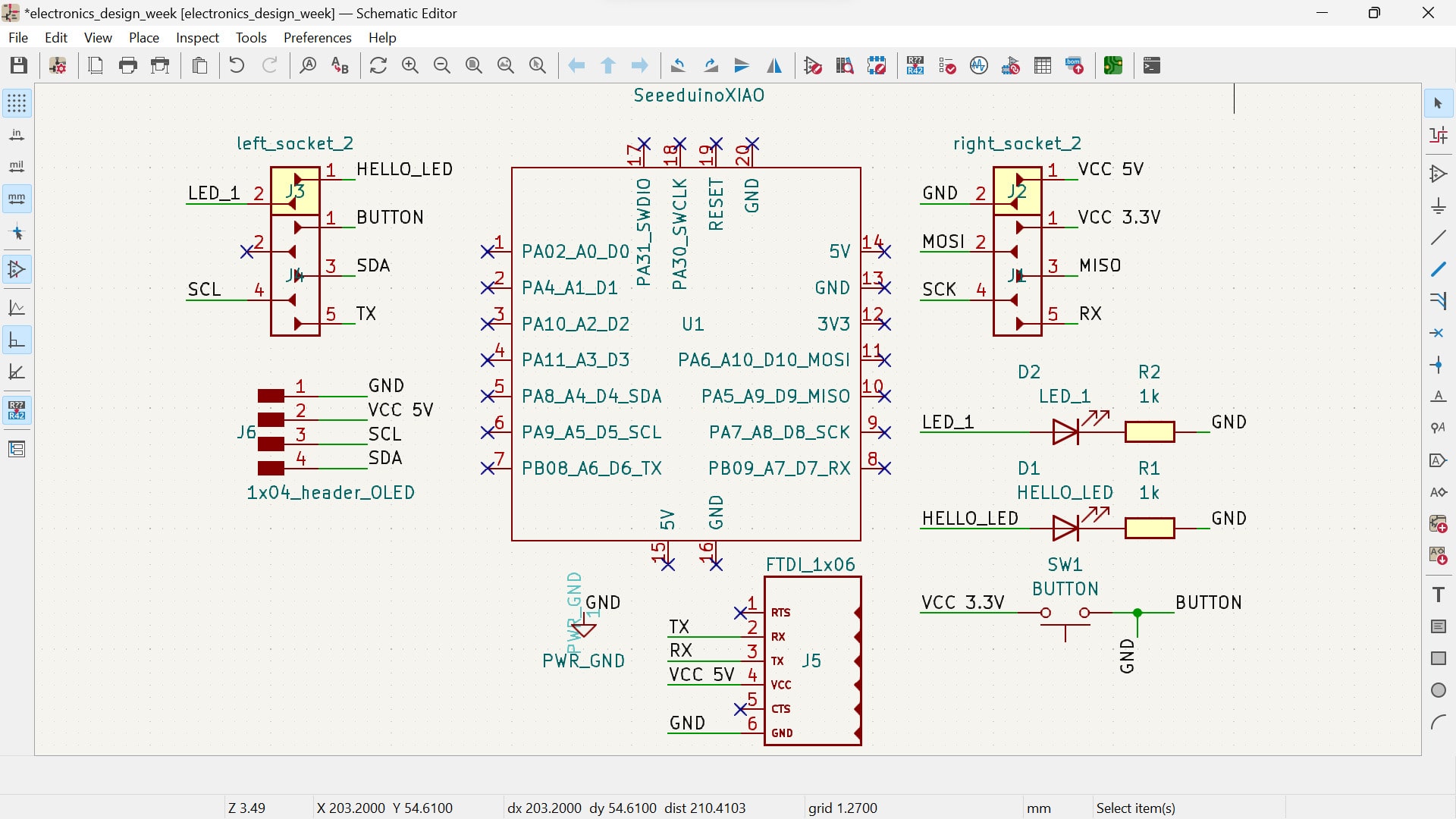
I made sure to utilize tags, and no-connection flags.
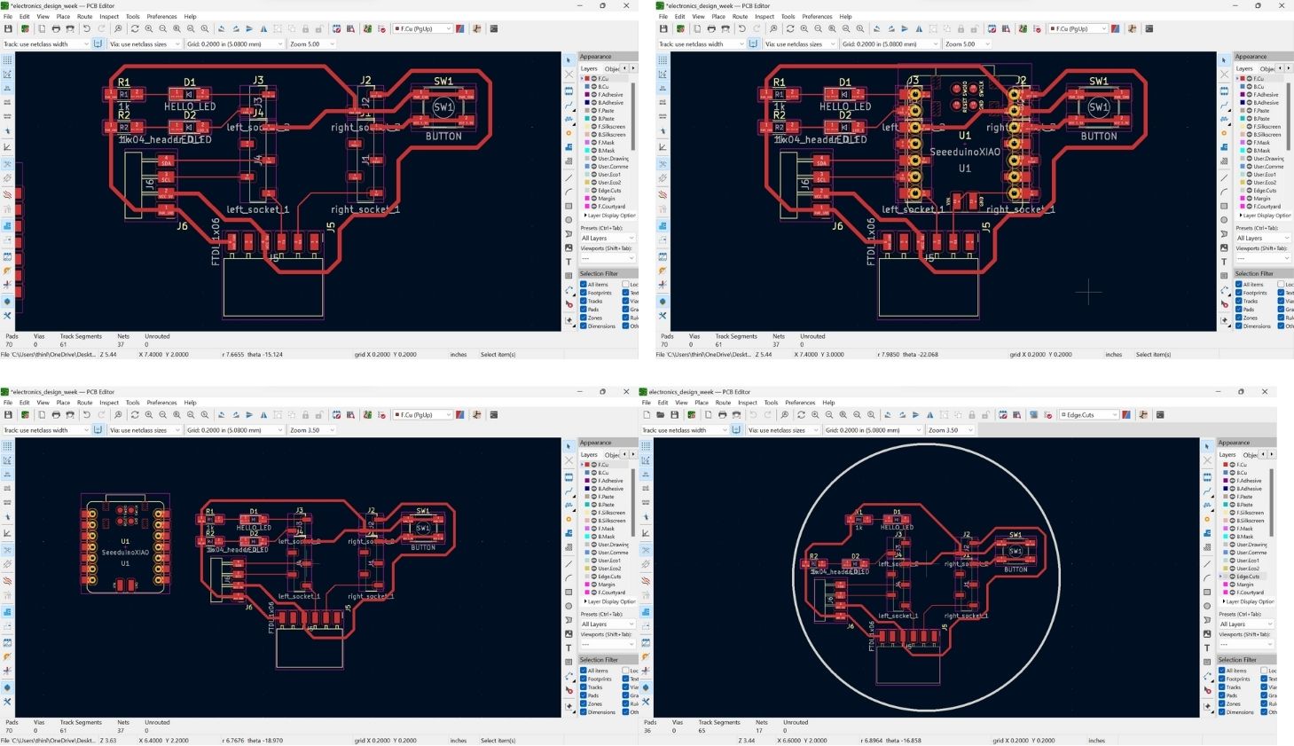
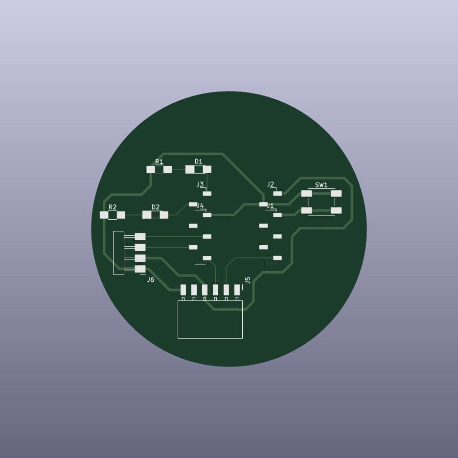
The PCB Editor
This week, I decided to try out something new and create a circular edge, so after I connected my components, I selected my “edge” material and then used the circle tool (at 0.6mm). For this week, my power lines were 0.6mm and my signal lines were 0.2mm.
I didn’t include my microcontroller footprint in the final export because I’ll be connecting it to the 1x07 connection sockets.
Design Rules & Constraints
Before designing a board, it’s important to set ‘Design Rules & Constraints’. These rules guide the design process, making sure that the board is made correctly and works as planned. They also take into account the tools used to cut the board, preventing any manufacturing issues.
Electronic Rules Checker (ERC)
In KiCad, the Electrical Rules Check (ERC) can be used to find and resolve electrical issues with your schematic. You can find this feature by clicking on the Perform electrical rules check button in the top toolbar. This tool checks for common mistakes such as unconnected pins or wires and incompatible pin types.Then it’ll generate a report detailing any detected errors and warnings, which you can then use to correct the issues !!
ModsCE
mods CE (community edition) is a fork of CBA mods research project. mods is a modular cross platform tool for fablabs. It is based on independent but interrelated modules.
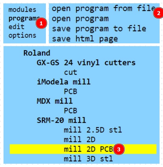
Our local instructor introduced this software to us in the past, so I was quite comfortable with navigation. However, here are the steps that I followed to prep my files for milling.
- Open the mods CE website.
-
After opening the page, do the following:
right-click> programs> open program> mill 2D PCB
(This last step can differ based on your local milling machine)
-
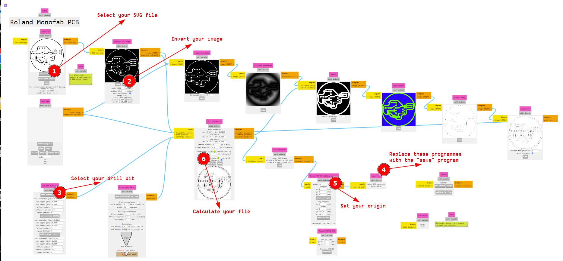
The following page should open up.
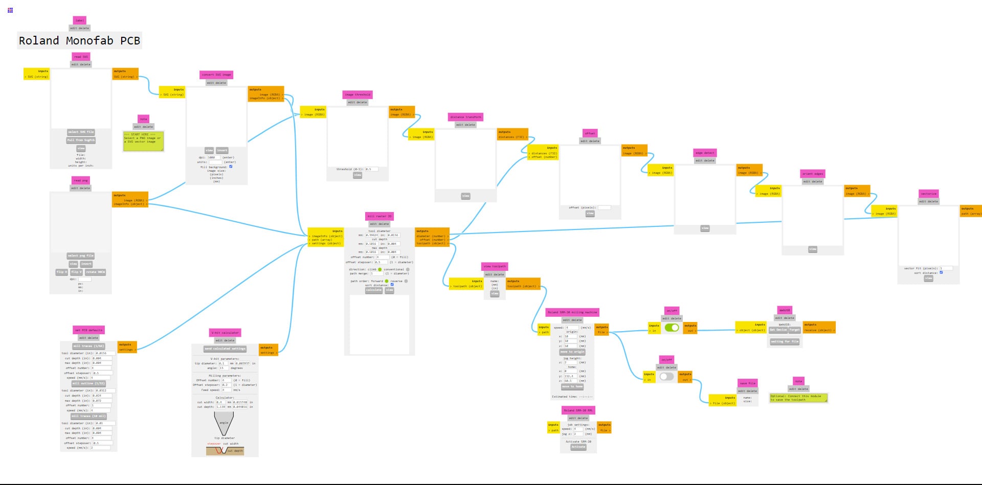
If it does, follow the instructions as shown below.
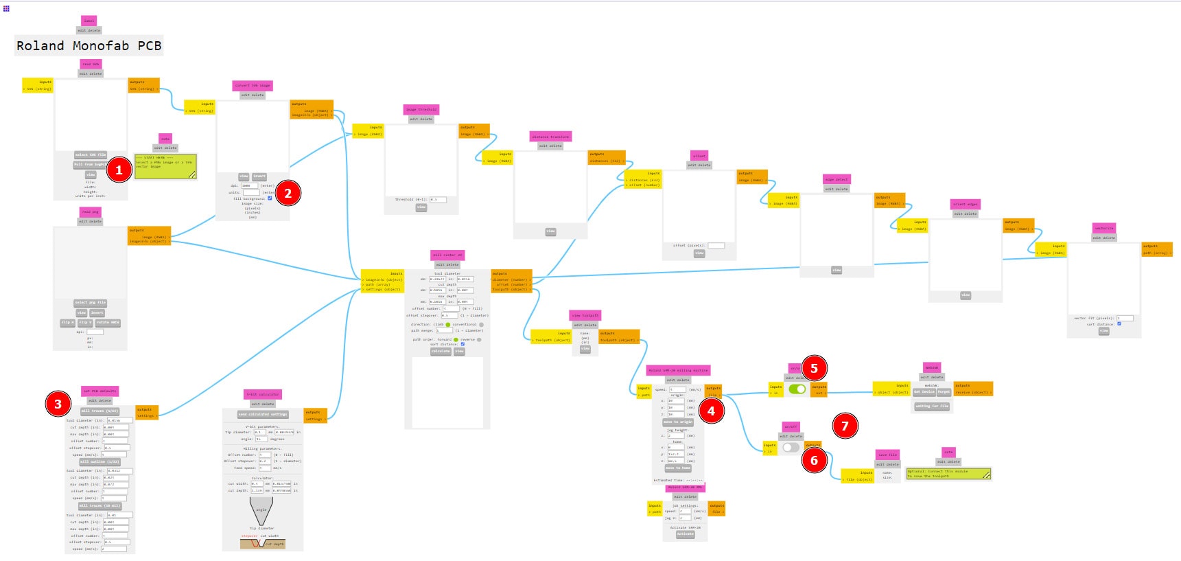
3.1 Select your SVG file.
3.2 Invert your image (refer to this page before doing so).
3.3 Select your drill bit. (reference) (This step can differ depending on your file. The 1/64 option is used for your circuit traces, and 1/32 for your interior cuts and drills.)
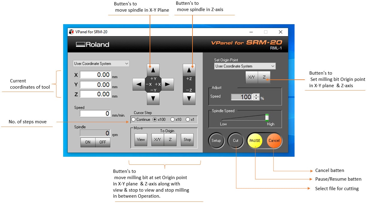
3.4 Set your origin. (reference)
3.5 Delete this program.
3.6 Delete this program.
3.7 Add a new program.
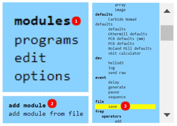
- right-click
- click on “modules”
- click on “add module”
-
click on “save” under the “file” tab
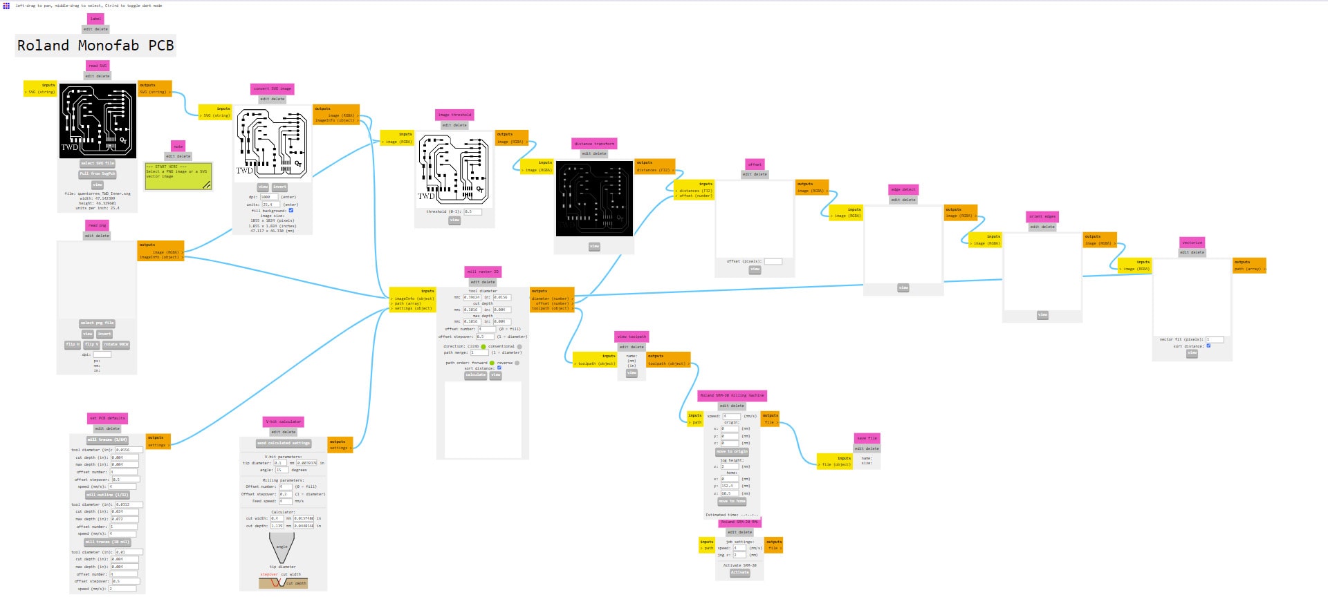
4. After you’ve followed the steps, your page should look something like this.
-
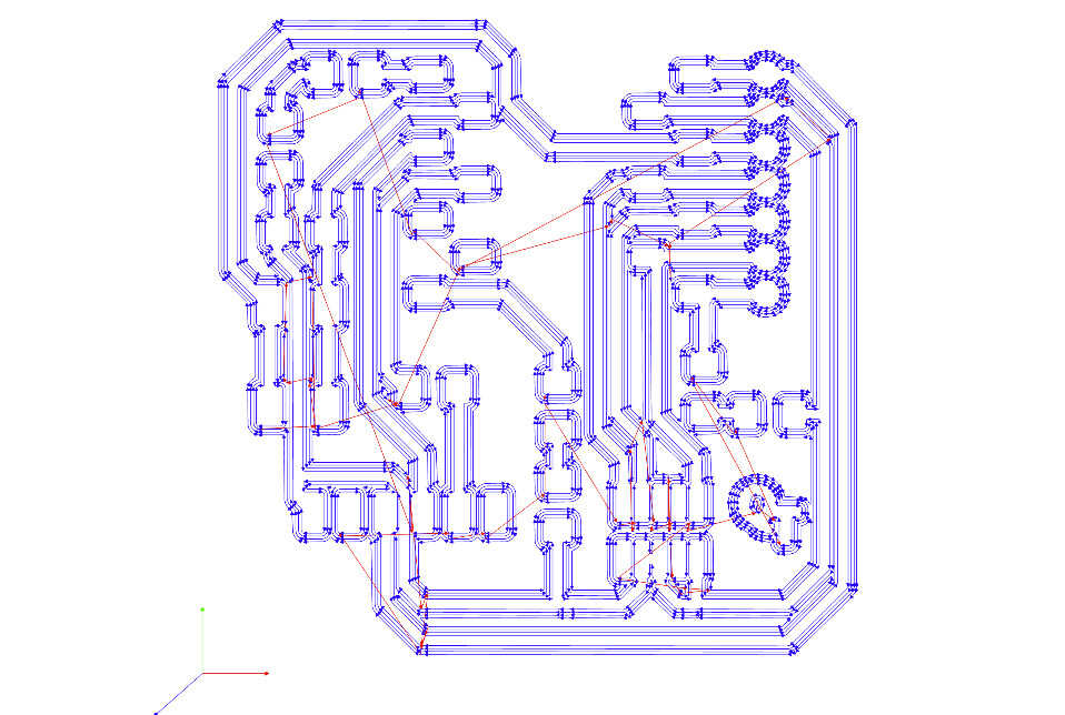
Click on calculate. If you’ve done everything correctly, your file should start downloading. Here’s a nice visualization of what a g-code looks like.
Important note !!!
Right next to the calculate tab, there’s a view tab that you can use to check out what your toolpath looks like. This is really helpful for checking if there’s any clear mistakes at a glance.
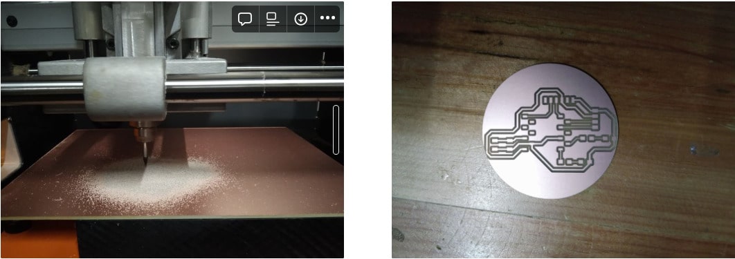
Milling
After the bed was set, I set up the milling machine, and started cutting out my files.
Soldering
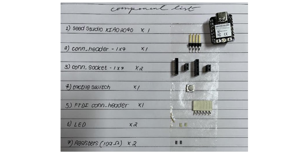
As usual, I started the soldering process by listing down all the components I needed.
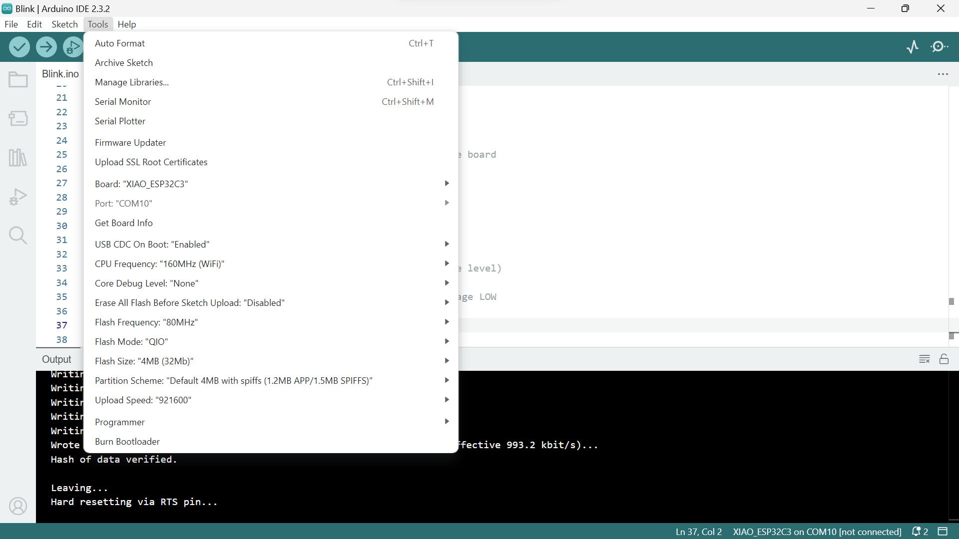
Programming
I decided to leave programming the OLED display for next week, so I programmed a simple blink code using Arduino IDE.
void setup() {
  // initialize digital pin LED_BUILTIN as an output.
  pinMode(2, OUTPUT);
}

// the loop function runs over and over again forever
void loop() {
  digitalWrite(2, HIGH);  // turn the LED on (HIGH is the voltage level)
  delay(1000);                      // wait for a second
  digitalWrite(2, LOW);   // turn the LED off by making the voltage LOW
  delay(1000);                      // wait for a second
}
I was also able to use my pushbutton as a circuit breaker.
PNG Renders
| Composite | Traces | Interior |
|---|---|---|
 |
 |
 |
click on the PNG render to access the SVG version on my remote repository for downloading !!!
This website was created using a template provided by Mr. Anith Ghalley and was used with his permission.*