Week 8 - Electronics Design
For this week, I decided to learn KiCad because of its user friendly interface. For the solo assignment board, I decided to create a board that I can use for many inputs and outputs but also for my final project.
Designing the board
Creating the schematic
Before I even started creating the schematic, I went and grabbed the KiCAD Fab library in order to get some starting parts.
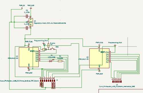
Then, I created a new project, imported 2 ATtiny412 chips, an LED, a button, lots of resistors, some pin headers, and went to town on it. Below is what I created after an hour of fun and pain.
PCB editor
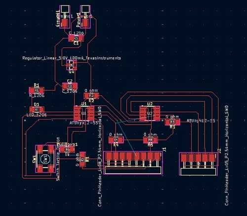
After I created the schematic, I entered the PCB editor and started laying out my components. Though I want to save space, my priority for this board is easy use and simplistic layout. Below is how I layed out the components.

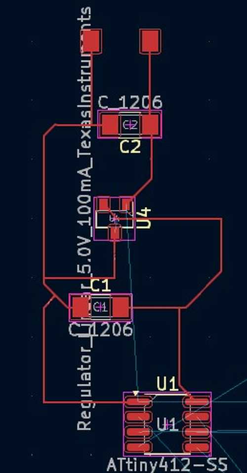
After laying out the components, I wired the power area for the chips. One problem I ran into was wiring the capacitors for the regulator. I couldn't find online how I was supposed to wire them so I re watched neil's video and found how he showed it being wired. I then proceeded with a different regulator so I could wire it like neil did and updated the PCB editor. Below is the wiring for the power supply.
Then, I went to work on wiring the rest of the ports, using 0 ohm resistor when needed, and wiring the components such as the LED and Button.
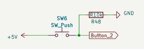
During this, I ran into many problems such as incorrect components, capacitor wiring, the schematic of the ATtiny not being the same as the actual ATtiny footprints, and more. Even push button schematics weren't working with how I imagined it. Luckily for me, I found this schematic only which explained where the pull down resistor should go.
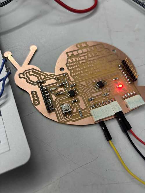
Finally, when I finished wiring the schematic as seen above, I used the keybind "d" to grab components with their traces and compact my board. My final PCB traces are below.
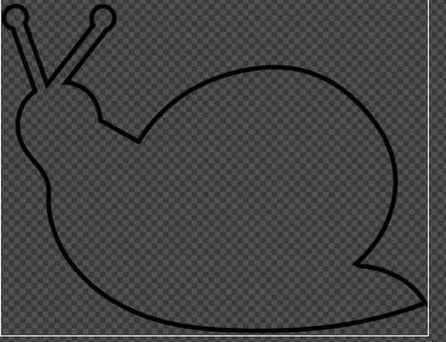
As you can see, the board looks like a snail, so I decided I would make the board cutout snail shaped as it took me awhile to create anyways.
Outline (still in PCB editor)
I first found a good snail image that I felt matched my board. Then I used inkscape to trace the snail and get it cut out of a big rectangle.

Then, I used some more inkscape tools and got a final 1/32 outline for my snail board.
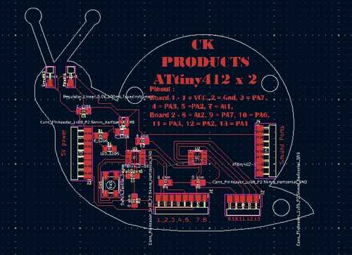
To insert the svg, I used the "add a bitmap" button in PCB editor and added it on the edge.cut layer instead of the Cu. layer. However, when I did that, the background came with so I used an online background remover and that worked.
Or not ....... so though the image imported with no background, it wasn't counted as a cutting line and I decided that I would trace the trace I made with the tools in KiCad. This arose another problem. KiCad doesn't have a spline tool, only lines, center arcs, and simple shapes like such. To bypass this issue I used the line tool in small increments and arc tool when i could. (I later learned that there was a special image converter tool in the main menu.)
After doing the outline, I added some labels to ports, logos, VCC ports, ground ports, and moved the components to fit nicely inside the snail outline. The amazing final result is below.
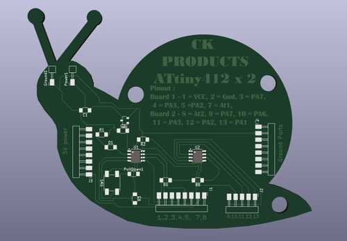
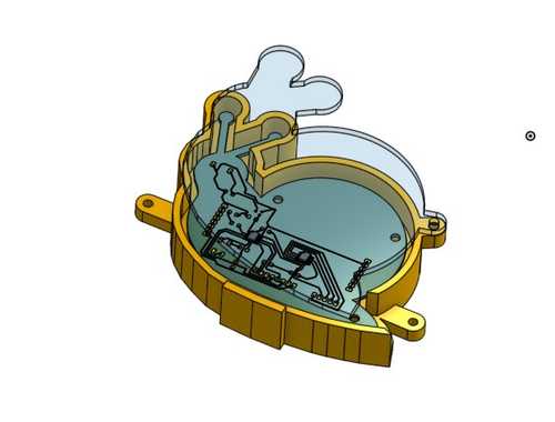
3D Version :
In CAD troubleshooting
To eliminate errors before I mill th board, I used the "design rules checker" in KiCad to ensure that there was no errors in my design. Luckily, I was pretty thorough when designing and had no errors other than some 0 ohm resistors which KiCAD didn't like for some reason.
Designing a case
Importing the board into onshape
I decided that I would make a snail case for my snail board. I used onshape to create the case as I am most familiar with the tools needed such as the "Use" and "Offset" tools in the onshape software.
However, as soon as I imported the snail as a STEP file, I ran into a problem. The snail file came in well, but it was missing the holes which were super important for the case so I had to find a solution for this.
My solution I came up with was to use an image and overlay it on top of the board to get the hole positions. This solution worked well and I moved onto the case design

Creating the Case
At first, I was planning to bring the board in to an assembly and use edit in context, however, I changed my mind and decided I could build the case in the same part studio the board came in to have a more organized document. The final result is below.
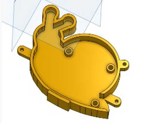
For the top of the case, I decided to CNC polycarbonate so I could see the LED's inside the board and easily access the button using a swinging mechanism as shown in the CAD below.
Milling and soldering the board
I won't go through a step by step of milling the board but I will explain some issues I ran into and how to deal with them.


Issue 1 - Trace Thickness
If you export a board from KiCad without changing the thickness of the traces, they will automatically be 0.2 mm wide, which when put on Bantam Tools, meant they were basically non-existent. To solve this issue, I went back to my KiCad file and did a "ctrl - a". Then, I went to select > filter. This allowed me to select only the traces on my board. Finally, I right clicked again and went to preferences to change the width of the traces to 0.5 mm
Issue 2 - Schematic Mess up
When I went to solder on the regulator to the PCB board, I checked the pinout for the regulator and UH OH.......... I wanted to cry, like not lying I was super annoyed.
The solution that I had to use was a external board that would hold my regulator and then use wires to route the correct pins to their areas. The reason why I had to use this solution rather than just re-milling my board was because the board took 40 minutes to mill and we ran out of 1/32 bits so I couldn't re-mill.
This is the horrid result my crying self added.

Sike! when I plugged in my board, I touched the regulator and it burned me. Because of this, I removed the regulator and fixed the board in KiCad for future use.
Final PCB Board

Group Assignment - Testing aspects of the board
Reflection
This week, I learned some amazing skills I could barely comprehend before. I learned the functions and capabilities of important components, how to create a schematic and then turn it into a PCB in PCB editor, and I also learned how to add images as outlines to make my designs even cooler. I plan to use this board on my final project as well as a fun board that has many uses at home.