   Propose a final project masterpiece that integrates the range of units covered,
      answering:
         What will it do?
         Who's done what beforehand?
         What will you design?
         What materials and components will be used?
         Where will come from?
         How much will they cost?
         What parts and systems will be made?
         What processes will be used?
         What questions need to be answered?
         How will it be evaluated?
  Your project should incorporate 2D and 3D design,
    additive and subtractive fabrication processes,
    electronics design and production,
    embedded microcontroller interfacing and programming,
    system integration and packaging
Introduction
Documentation for this week should be pretty easy, since I've already done a bunch of this work over the course of the semester. I'll be copy-and-pasting from my final project page and various weekly assignments as appropriate, and new text written this week will also be added to the final project page. So expect some duplication.This week I will also make progress on electronic design and system integration. Hopefully all key design processes will be complete by Wednesday of this week.
Function
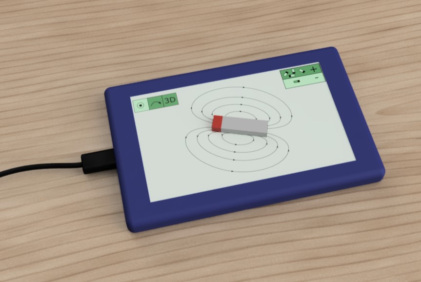
I'm a physics professor who teaches electricity and magnetism almost every year. My final project will be a device to let students see invisible magnetic fields. The device will be about the size and shape of a smartphone or small tablet, and will use a large array of magnetic field sensors to map out the strength and direction of magnetic fields passing through it. It will have a screen to draw and display magnetic field lines and vectors. As a basic goal, the device would show the strength and direction of the fields passing through it, so you would place magnets directly on or underneath it and it would draw the field as either lines or 3-d vector arrows.As a stretch goal, I'd like to create a true "camera", where you can point the device at one or more magnets some distance away, and it would show the magnets and their field lines as a 3-d visualization on screen. I have done some calculations to show that this is theoretically possible with the device I'm designing, but implementing this may require a later "spiral development" cycle that takes place after Fab Academy has finished.
Design Choices
Here are a few of the design decisions I've already made oover the course of the semester, that will form the core of this project.- Sensors: 24 TMAG5273 3-axis Hall effect sensors.
- Microcontroller: Raspberry Pi Pico RP2040
- Power: USB-powered
- Display: 480x320 TFT display
- User Interface: Touch screen
- Computer Interface: none, standalone device. (Stream serial data if needed?)
- Physical controls: no buttons, just plug it into USB and it starts.
- Case: 3D printed
Prior Art
There are some old-school non-electronic ways of visualizing magnetic fields, and some research groups have developed arrays of magnetic sensors, but I have not found any commercial product that does what I'm proposing to do, and the "camera" angle seems to be entirely new.
 An old-school way of visualizing magnetic fields is to sprinkle iron filings on a piece of paper resting on the magnet, but this has several limitations:
- It shows the orientation of field lines, but not their direction (north to south or south to north)
- It only shows orientation in the plane of the paper, not fields pointing into or out of the paper
- It doesn't show changing fields in real time
- It doesn't show a 3-dimensional view of the field surrounding the whole magnet
- It's messy.
Several engineering research groups have done some work with arrays of magnetic sensors.
- Texas Instruments provides some information on how to use an array of their Hall Effect sensors to detect the position of a magnet, but the goal here is to find the position of the thing the magnet is attached to, rather than to investigate the magnet's field.
- Zhang et al (2019) use a linear array of sensors to map out the magnetic field of a free electron laser undulator line, but they don't do a 2-d array, or visualize the field lines.
- Lee et al (2021) create a small 3x3 Hall effect array and use it to map out field strength, but not direction, and their device has only a few sensors.
I was unable to find anything that attempted to identify field sources from a distance, aka a true magnetic field "camera".
Work Completed So Far
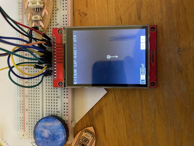
- I have gotten a TFT display working for Output Devices week.
- I have gotten a magnetometer working for Input Devices week.
- I have gotten a touchscreen display working for Interfaces and applications week, and implemented a simple touch GUI.
- I have written an application that integrates touchscreen, magnetometer, and TFT display to show the magnetic field from a single magnetometer, with a touch GUI, in Interfaces and applications week.
Design Considerations
I2C address programming
The key challenge is how to get the microcontroller to talk to 24 different magnetic field sensors simultaneously. I've thought carefully about how to do this. I plan to use both I2C interfaces on the RP2040, and to use the TMAG5273A1, TMAG5273B1, and TMAG5273C1 magnetometers, which are identical except that they have different default I2C addresses. The I2C addresses are re-programmable, but the chips need to be turned on in sequence, be assigned an I2C address, then turn on the next set. The initialization sequence will be as follows: I2C_interfaces = [0,1]
Model_numbers = [A,B,C]
chip_banks = [1,2,3,4]
For each bank in chip_banks:
Power on bank
For each interface in I2C_interfaces:
For each model in model_numbers:
Reprogram I2C address for chip at interface, model
Confirm I2C address change
Wait a bit
To power on the banks of magnetometers, I'll just be using the microcontroller's GPIO pins to provide power. The magnetometers use 3 mA of current when actively collecting data, and nanoamps when they're not, so the GPIO pins should be able to provide that easily. I'll add a buffer capacitor to each power line just in case.
I considered other options, such as an I2C output expander or a shift register, but these increased part count and circuit complexity by quite a bit, and these devices often need pins to control *them*...
Pin counting and microcontroller choice
With that system decided, I was able to figure out how many GPIO pins I would need for all features, including the TFT display, the touchscreen, and to power everything. I made a table of the resulting pin counts for each option.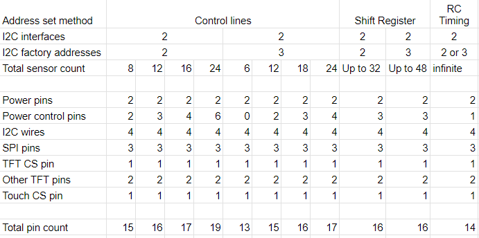 The outcome of this analysis is that I can't use a Xiao board for this project: it only has 14 pins, which isn't enough. I decided on the Raspberry Pi Pico, which is slightly larger in size, costs the same, is also solderable onto a custom breadboard, and includes about 30 GPIO pins.
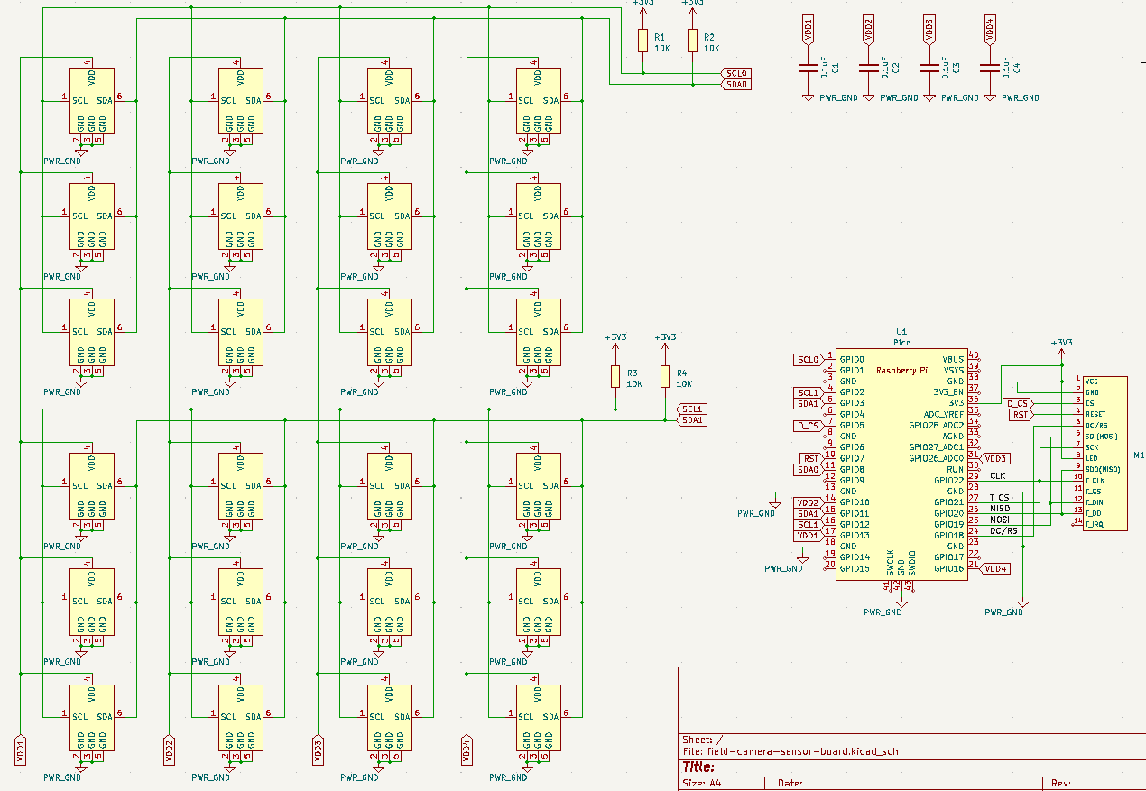
PCB design
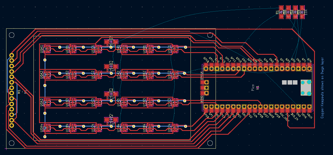
Another important design consideration is that this circuit board is going to be complicated enough that routing on a single-layer board is impossible. I could use zero-ohm resistors, but I'd need dozens of them. I'm going to take the plunge and try to make a 2-layer board. I'll design it in such a way that the back side of the board has a minimal number of traces. That way if I can't get 2-layer PCB manufacturing to work, I can just solder wire into the vias and use that to make the backside connections. I'm making progress with circuit board design, but it's not quite done yet. The tradeoff between aesthetics and clean PCB design is really difficult. Here's what I've got so far:
Mechanical Design
Mechanically, the project wil be a 2-layer stack, with the TFT display module on top, and the board containing the sensors directly underneath. The Raspberry Pi Pico will be slightly off to the side, so the whole area of the display can have sensors under it. For prototyping, I'll attach the screen and the Pico using female 0.1" headers, so they can be removed. That will allow me to test and modify the board if I have to. Once everything is working, I'll solder the display in directly, so the device is as thin as possible and the displayed field arrows are as close to the actual sensors as possible. The case will be a simple 3-d printed box. I haven't designed that yet but it's no big deal.

Magnetic Field Interference and Calibration
There are a bunch of things I'll need to worry about to get an accurate measurement. First, the device can't have any iron or steel in it: these will distort the field lines dramatically. Annoyingly the TFT display comes with an unnecessary SD card slot which is probably steel: I'll try to desolder this if it is. I will also use nonmagnetic brass or stainless steel screws to hold the case together. The USB port has a small amount of steel in it: nothing I can do about that.
Second, if I solder the magnetometer chips on crooked, they'll report the wrong direction for the magnetic field. Rather than trying to be impossibly precise, I'll fix that in software with a calibration procedure. My physics department has a Helmholtz Coil that can produce a uniform magnetic field of known strength: I'll use that to calibrate the sensors to compensate for any misalignment or bias.
Materials
My project will use the following parts:- Raspberry Pi Pico RP2040. Qty 1 @ $5.75
- LCD Module Touch Screen ILI9488 480x320 3.5in. Qty 1 @ $18.69.
- TMAG5273A1QDBVR 3D Hall-effect sensor. Qty 8 @ $1.56
- TMAG5273B1QDBVR 3D Hall-effect sensor. Qty 8 @ $1.62
- TMAG5273C1QDBVR 3D Hall-effect sensor. Qty 8 @ $1.62
- FR1 Copper Clad - Double Sided 4x6in. Qty 1 @ $1.88
- 1206 SMD 0.1 uF capacitors. Qty 4 @ basically free.
- 1206 SMD 10k resistors. Qty 4 @ basically free.
Manufacturing
Manufacturing steps:- Finish board design.
- Mill prototype board.
- Install just enough sensors to test I2C address reprogramming.
- Solder prototype board.
- Test field sensing without GUI.
- Modify existing touchscreen GUI to work with 24 sensors.
- Rebuild / modify board to remove pin-and-socket header connections, permanently solder TFT display.
- Design case
- Print case
- Final assembly
- Next spiral: draw field lines as lines rather than arrows.
- Next spiral: 3-d "field camera" mode.
Open Questions
- Will I be able to get double-sided PCB milling working? I have a backup plan to manually solder wires if not.
- Will the I2C address reprogramming scheme work? I will do a test run first.