Week 6: Electronics Design
Checklist for this week:
- ☑ Linked to the group assignment page
- ☑ Documented what you learned in electronics design
- ☑ Explained problems and how you fixed them
- ☑ Included original design files (Eagle, KiCad, etc)
- ☑ Included a 'hero shot'
Group Assignments
- Use the test equipment in your lab to observe the operation of a microcontroller (MCU) circuit board (as a minimum, you should demonstrate the use of a multimeter and oscilloscope)
- Document your work on the group work page and reflect what you learned on your individual page
Individual Assignments
- Design a development board to interact and communicate with an embedded microcontroller
Reflection on Group Assignment
Multimeter is a must-have equipment for physical electronic design and trouble-shooting. It is used to measure voltage, current, resistance and continuity (meaning whether there is current flow in the circuit).
Design PCB using Autodesk Eagle
Autodesk Eagle is an Electronic Design Automation (EDA) software package that allows users to create electronic schematic diagrams and printed circuit board (PCB) layouts. There are other alternative EDA software like KiCAD and SVG-PCB (Browser based) but Eagle is one of the most popular tool so it's easier to find helps online and offline.
Generally we went through the following steps:
- Study PCB produced from previous course cycles
- Creating our own schematic using EDA
- Wiring components together with
net(R) and then Electrical Rules Check (ERC) - PCB layout using
route manual(R) and then Design Rules Check (DRC) - Export for milling, from
pngtoG-codethrough mods in a browser.
Downloading and Installing Eagle
The good news is that Eagle EDA comes within Fusion 360. There is a standalone software but we already have Fusion 360 installed previously. We just need to open (start) a "New Electronic Design" project. Before we start to design anything on the working area, import libraries into Eagle.
Add fab.lbr (original from FabAcademy, revised by Mr. Steven Chew) and xiap_rp2040.lbr (from Seeed Studio) to the library of Eagle (within Fusion 360).
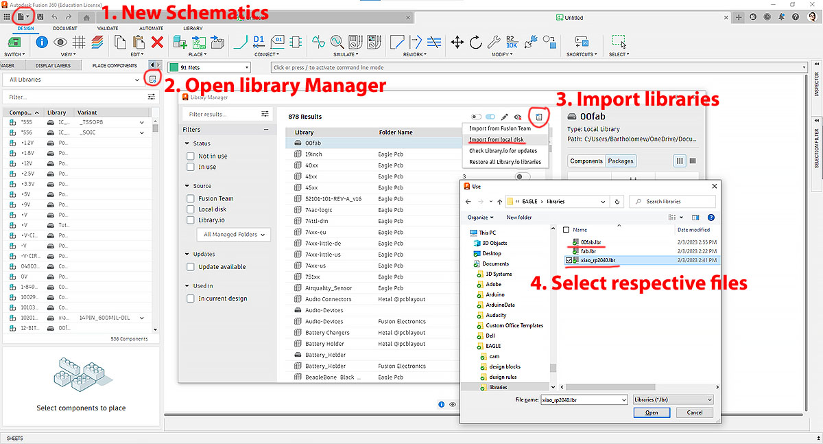
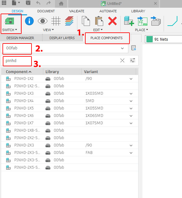
There are 3 (switch) modes on the top left design buttons: Schematic document, PCB documents and 3D PCB. The idea is to place components in the working area and then "net" (shortcut "R") the components to the MCU. Switch to PCB document and then route the path to components.
In the "Place Components" panel on the left, we could easily search for the component like XIAO_RP2040, PINHD-1X5, PINHD-1X6, PINHD-1X7, GND, VCC-CIRCLE, Resistor, etc. Double-click on the list to select it and place it in the work area. Use the net tool to link the components.
You could right-click for more menu and change the names of the components or wire. Once the schematic document is done, switch over to PCB layout document (Top left button) after ERC check (under "Validate").
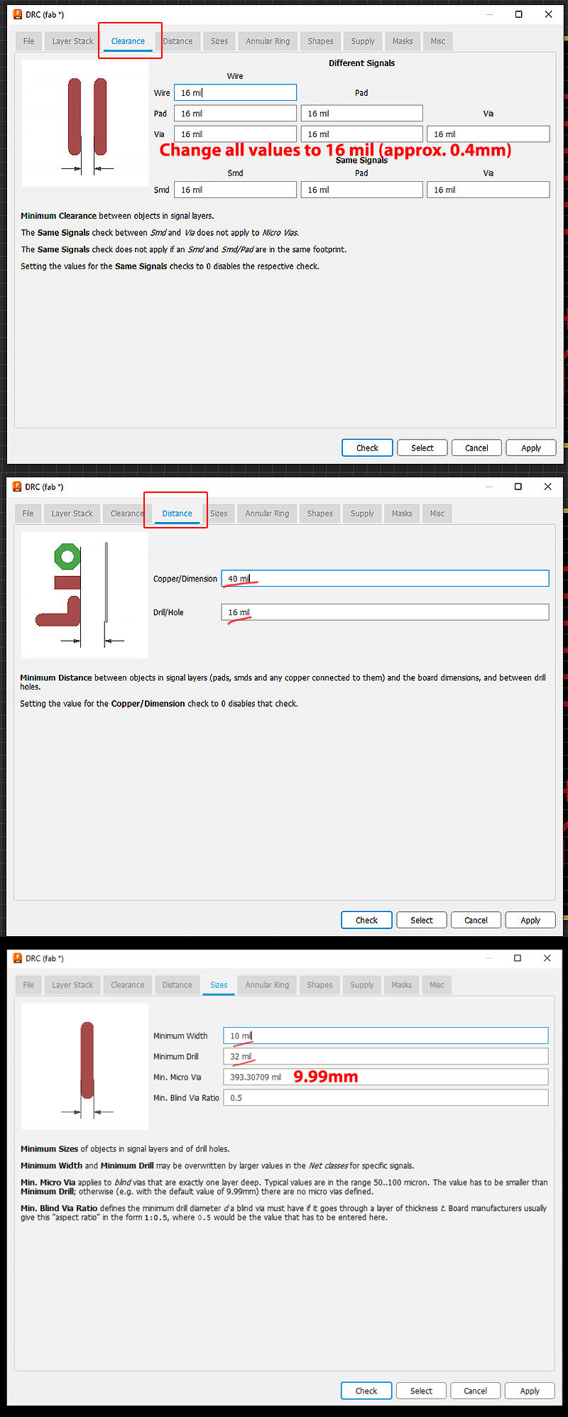
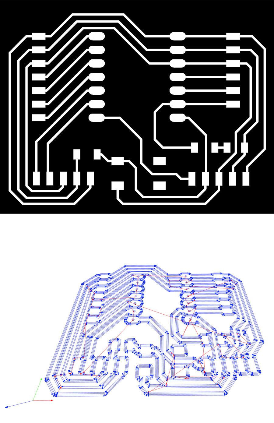
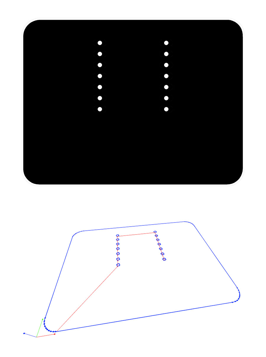
Layout all the component within the "Board Shape" and then use route manual (shortcut key "R") to link all the components that pass the DRC check. While you could import fab.dru but it's easier to change the numbers directly (picture below).
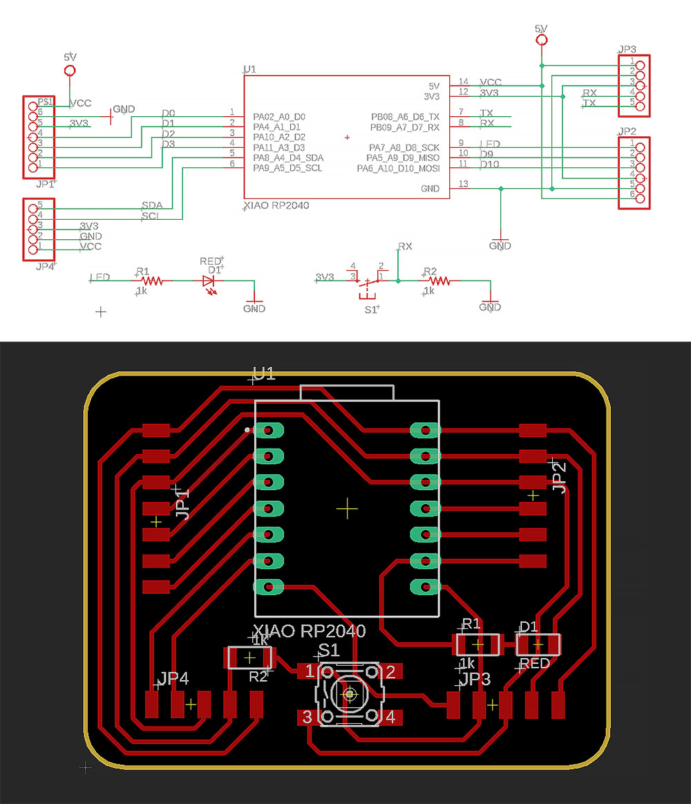
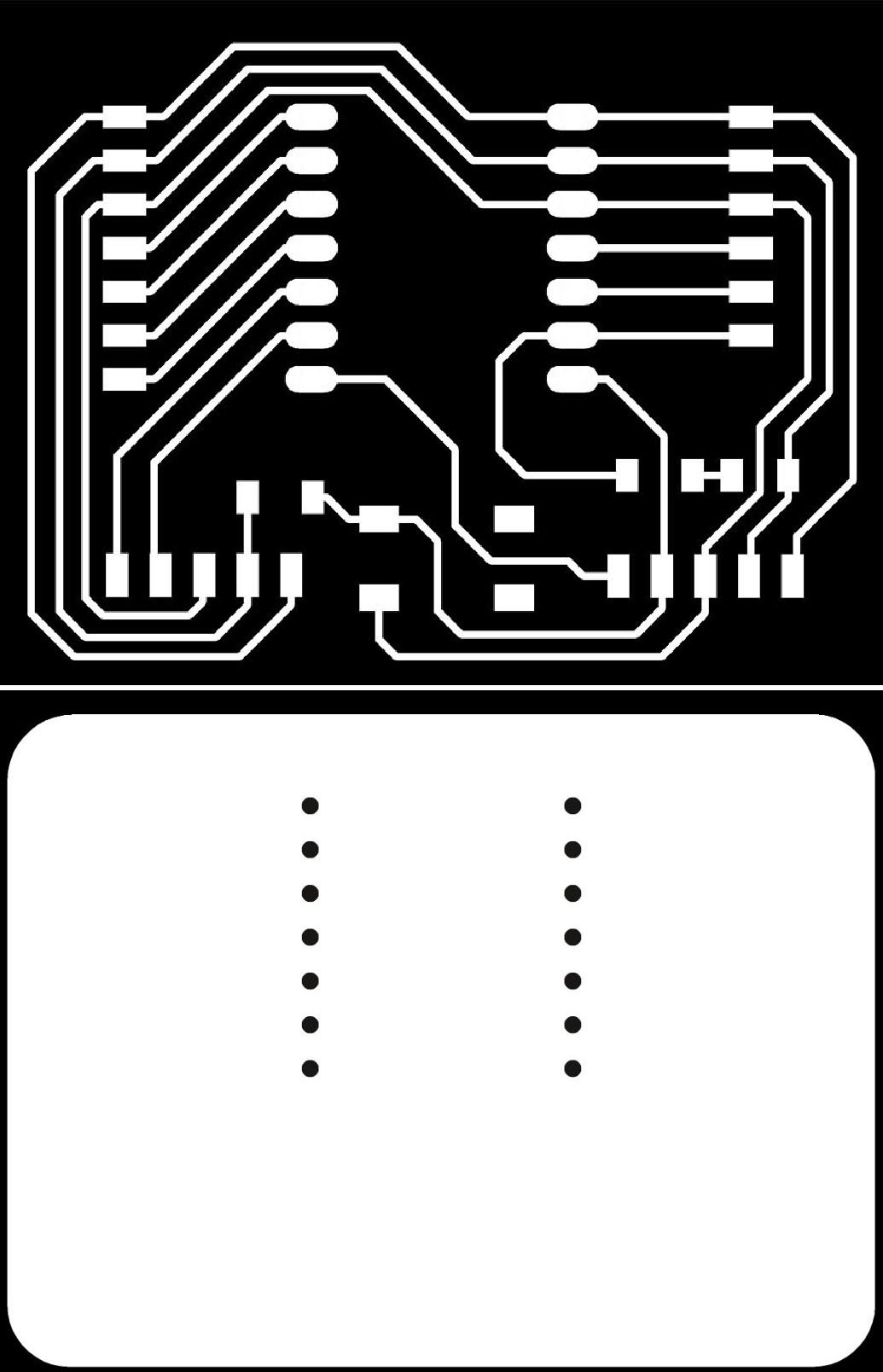
Final Schematic and PCB layout
The schematic mainly inspired by Steven's design. He guided us first half of the assignment and we figured out on our own how to complete the final parts as some of us are quite fresh. The different is the re-arrangement of the 3.3V, GND and 5V pin on the bottom left.
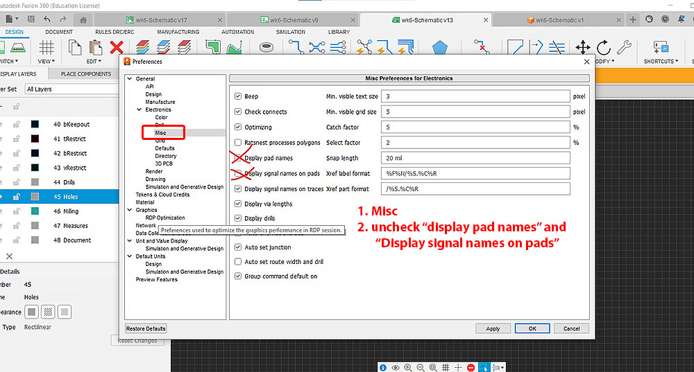
Issues while exporting Image (PNG) and how to fix it!
While we are designing the layout, all the layers are turned on by default. But during export all the additional texts on every other layers complicated the final image. While looking back it's quite an easy solution, but to really dig into the preference menu and uncheck certain boxes (pad and signal names) test the user-friendliness for all beginners. Luckily, we have experienced instructors to point them out for us.
So here is another tip for beginner: before you start using Eagle, always identify experienced user around the proximity (or someone you could approach easily) goes a long way!
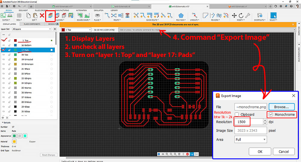
Final step in Eagle is to type "export image" in the command bar. As mentioned earlier, go to the user "preferences" and unchecked the "pad and signal names". On the display layer panel (left hand side), turn off all the unnecessary layers (picture below). Keep only layer 1 and 17 to be displayed. Do a second "export image" if you are milling holes by turning on layer 17 (Pads) and layer 20 (Dimension). Remember check the box "monochrome" during export.
With the PNG exported, we could use raster image editing software to finalize the layout before generating G-code.
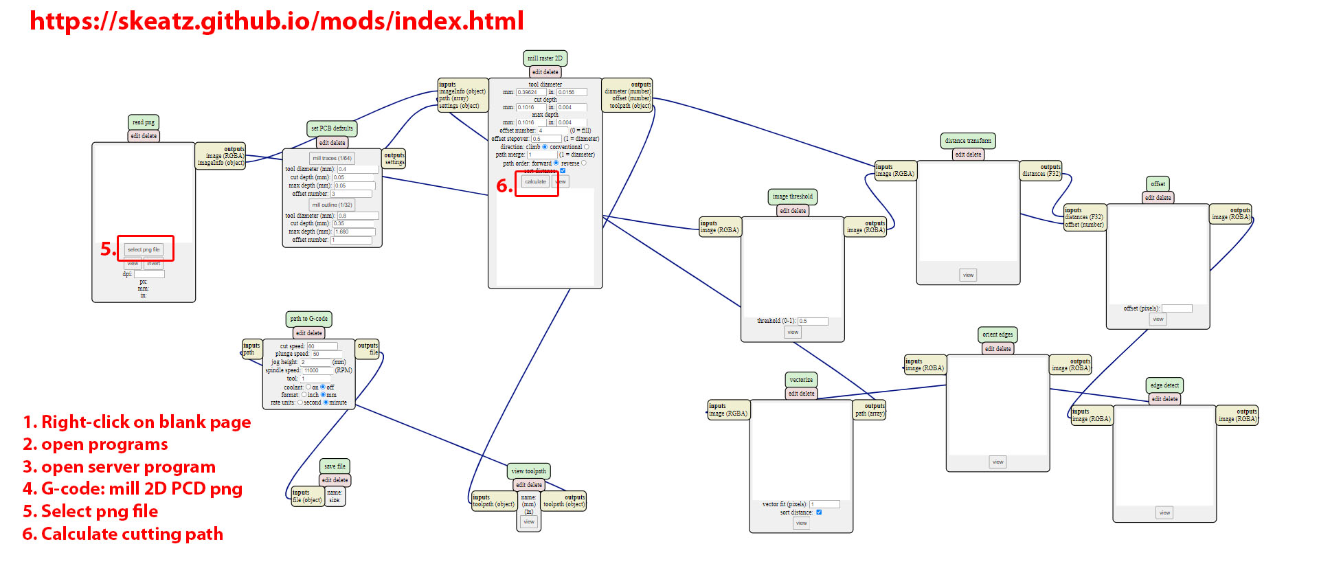
Generate G-code in browser
Once we have the png files, we go over to mods to generate the G-code. The G-code will be downloaded to your local hardisk in NetCDF format file (.nc)
We will be milling the PCB in two weeks time in next assignment.
Hero shot
Update: Exciting chapter following on Week 8 (Electronic Production)
Topics covering milled circuit board (mill more than 8 more board and counting!), Electronics components with SMD soldering process (Flexing my memory muscle and trying hard to improving soldering skill), Testing process (continuity test on multimeter), Trouble shooting process (multiple re-soldering), and finally interact and communicate with an embedded microcontroller