8. Electronics Production
Printed Circuit Board production week includes producing the PCB we designed in our previous assignment i.e from Week 6: Electronics Design . Before that let's go through some basics of PCB and PCB production.
What is a PCB?
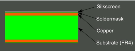
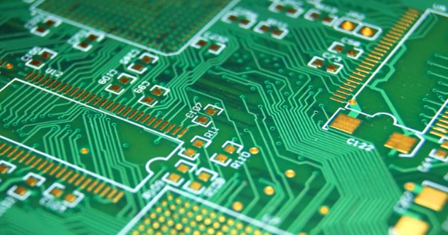
A printed circuit board (PCB) is an electronic assembly that uses copper conductors to create electrical connections between components.The structure of a PCB:
Conductive features on printed circuit boards include copper traces, pads, and conductive planes. The mechanical structure is made up of an insulating material laminated between layers of conductors. The overall structure is plated and covered with a non-conductive solder mask, and a silk screen material is printed on top of the solder mask to provide a legend for electronic components. After these fabrication steps are completed, the bare board is sent into printed circuit board assembly, where components are soldered to the board and the PCBA can be tested.
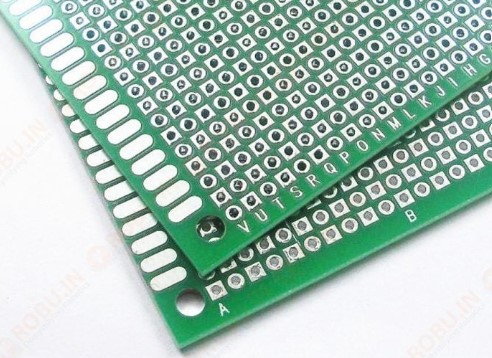
Types of PCBs
The various types of PCBs can be listed as follows:PCB Production techniques
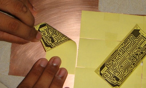
I had previously used General purpose circuit boards, and even ordered etched PCBs, but just realised that the machine we have is a PCB milling machine and is completely different type of production method. That triggered me to explore all types of PCB Production techniques. Here's what Moko Technology lists: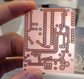
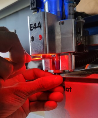
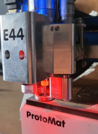
Using Protomat E44
Our FABLAB has Roland SRM 20, but it is under maintenance. So we used another milling machine that we have at our lab, Protomat E44 Circuit Board plotter from lpkf.com.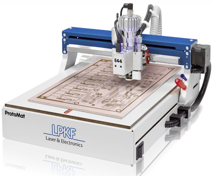
Step 01: Installing LPKF software
The software you need to have installed on your PC for connecting with Protomat E44 is LPKF Circuit Pro PM . The installation process is pretty intuitive.
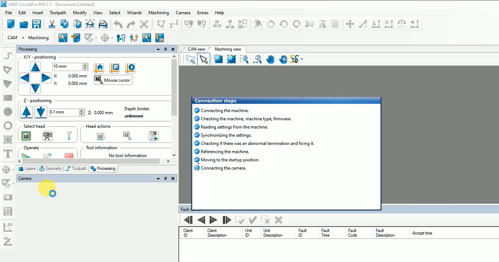
Step 02: Setting up the machine
Once the software is opne, it itself tries to find the machine (just make sure the machine is turned on and wired to the laptop) The interface looks as shown below and it takes few minutes to set up the machine, home the end effector and reference the machine overall.
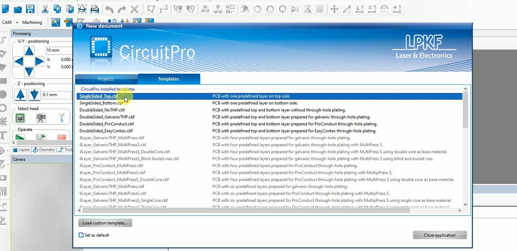
Step 03: Start a new document
Start a new document and choose the template based on the design of your PCB.
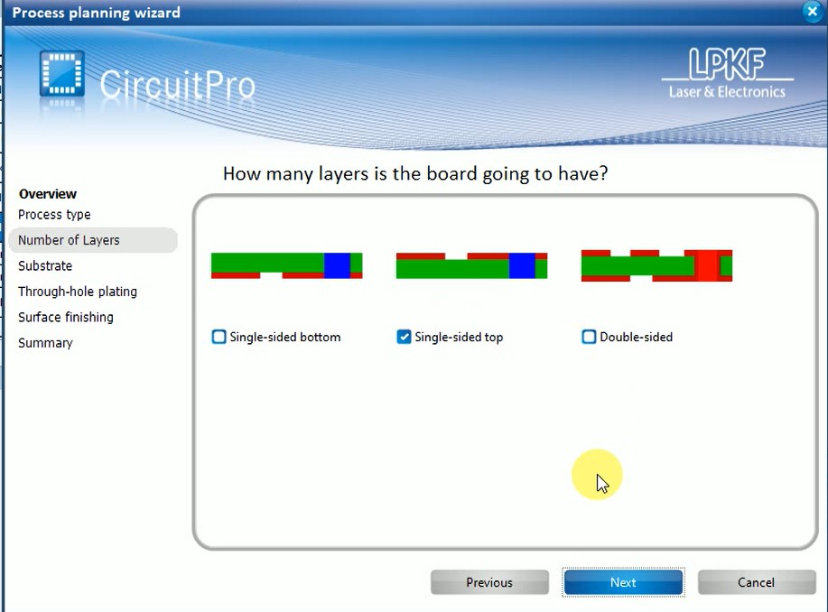
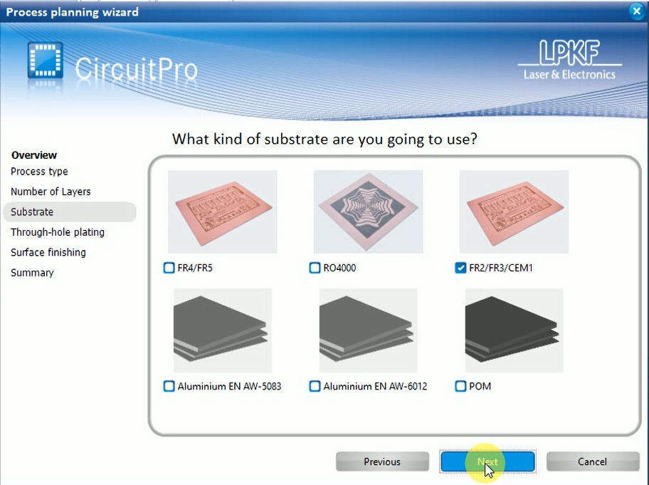
Step 04: Open process planning wizard
As shown below, open the process planning wizard.
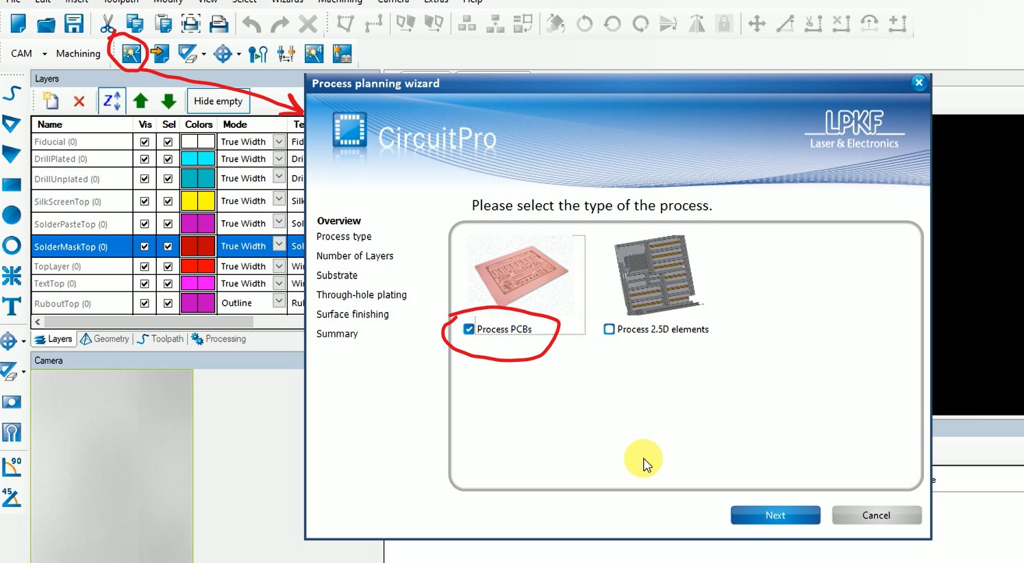
Choose the right options as shown in the images below for the process, single or double sided PCB, and substrate selection.
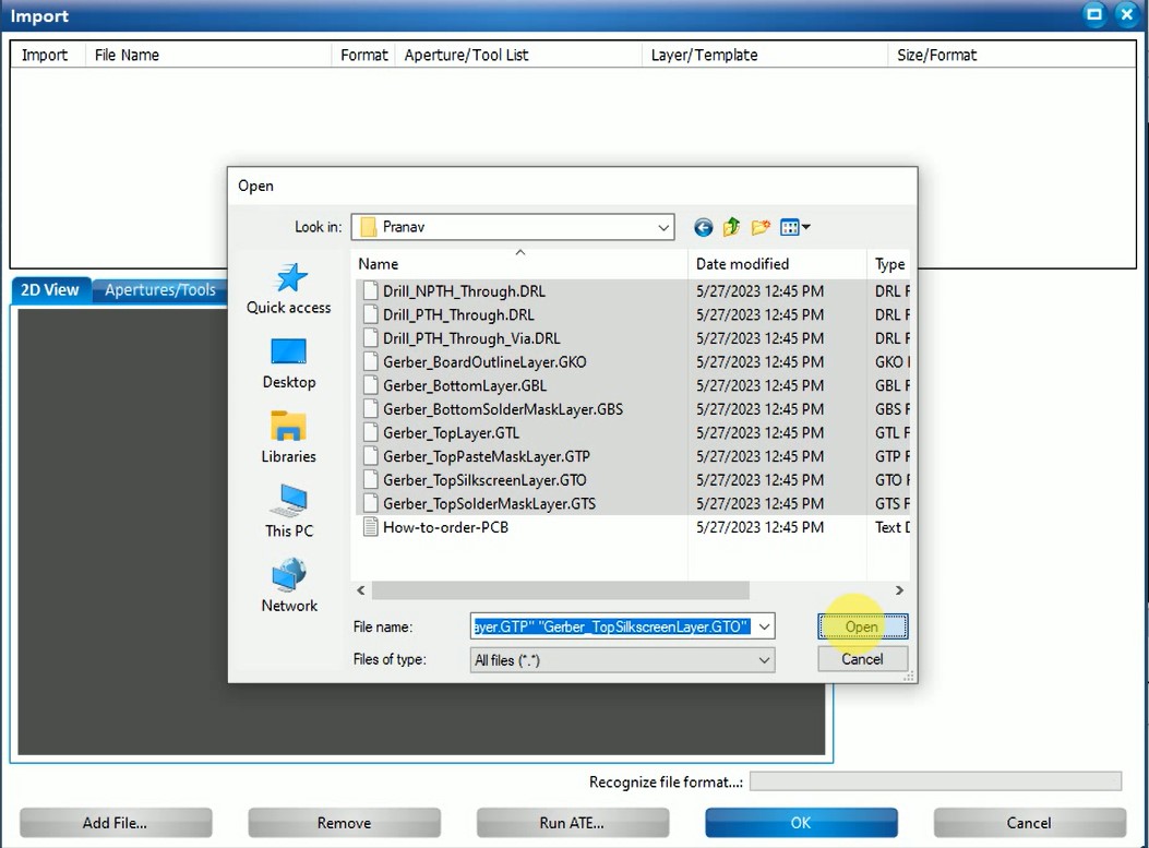
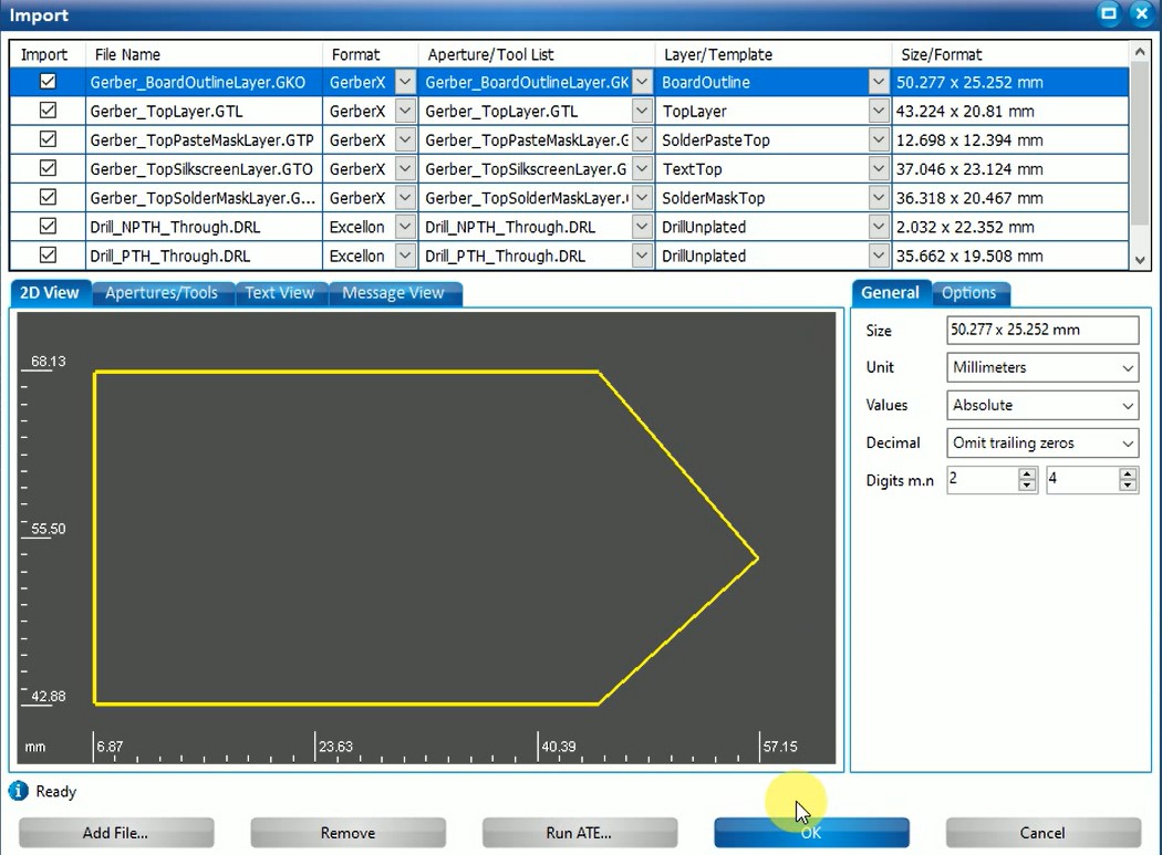
Step 05: Import Gerber file
Once that is set, go to files > import and then locate your gerber files and import them.
This is where we went wrong into properly selecting what exactly needs to be imported. We learnt it the hard way that, basically if it is a single sided PCB, you only need the following:
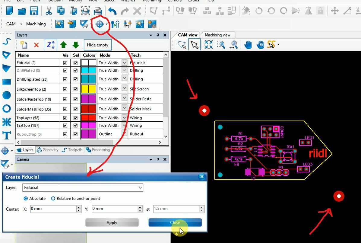
Step 06: Create fiducials
Now you need to define the end to end diagonal marks as fiducials to limit the space claim of the design on your copper plate. THis can be done as shown below:
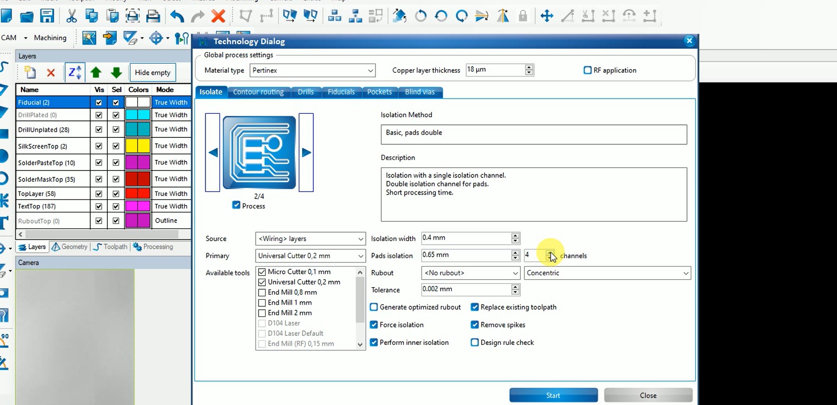
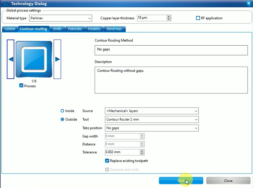
Step 07: Generate isolation and contour routing
Open the dialogbox as shown in the figure below. Here you need to define the isolation type, width, and number of channels. Very important steps. So basically this is where you define how muh isolation you want between two conducting lines.
I tried multiple variations such as 0.2mm width and 2 channels, 0.4mm width and 2 channels, 0.4mm width and 4 channels and even 6 channels. The most efficient one acording to me in terms of functionality as well as time consumtion was 0.4mm width and 4 channels. And the contour to select is no gap contour. Rest all settings can be left as it is as default settings.
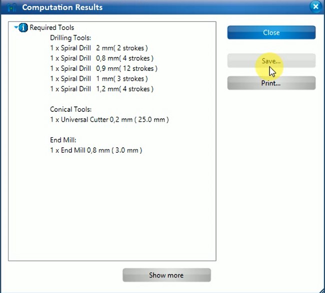
Once this all is setup and we click next, the overview of the types and number of tools are needed is showcased as shown below:
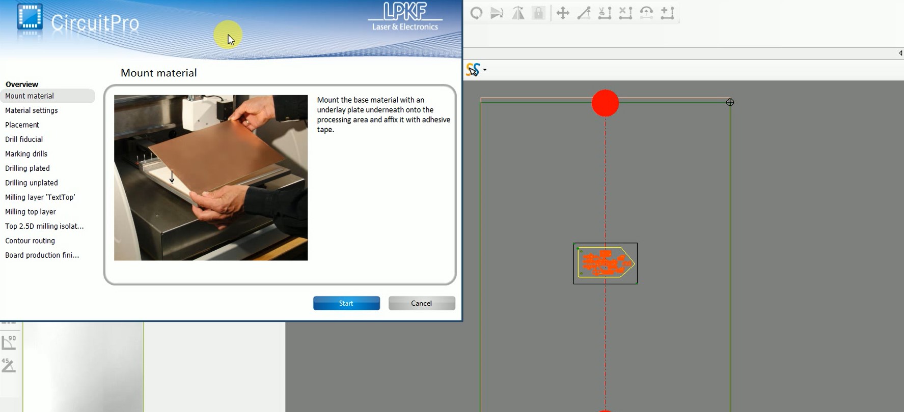
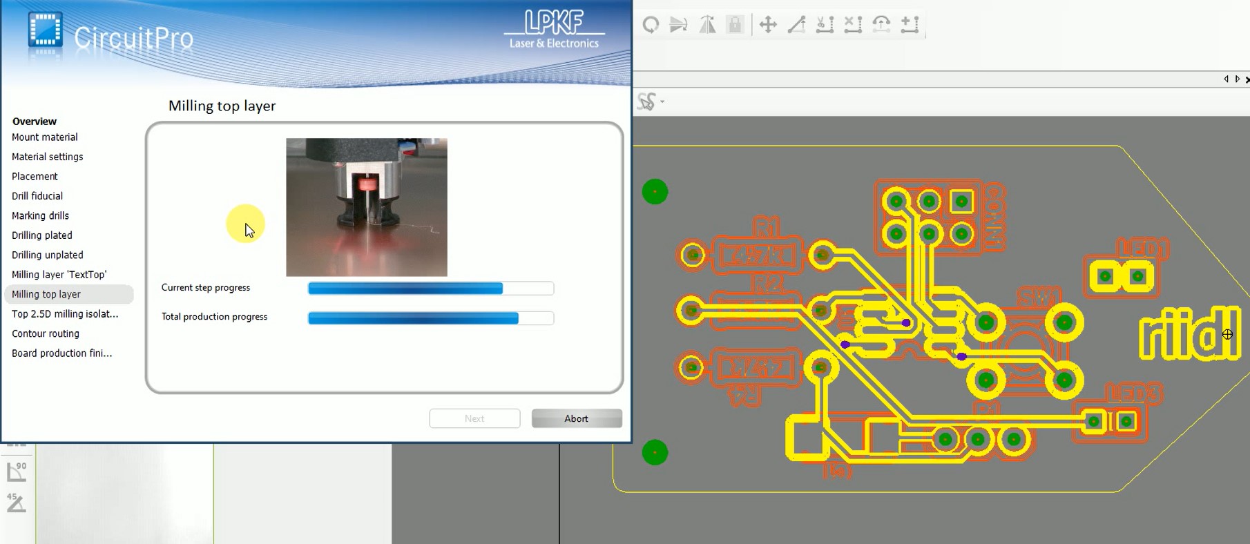
Step 08: Start board production wizard
Once everything is set, we start the board production wizard as shown in the figure below.
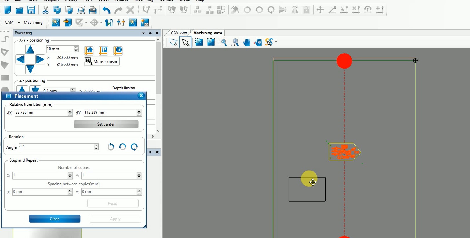
Step 09: Define PCB placement
To define the placement of the PCB on the copper plate, we go to Machining > Placement and then just drag and drop the rectangle define dby the previously marked fiducials to the desired location on the copper plate.
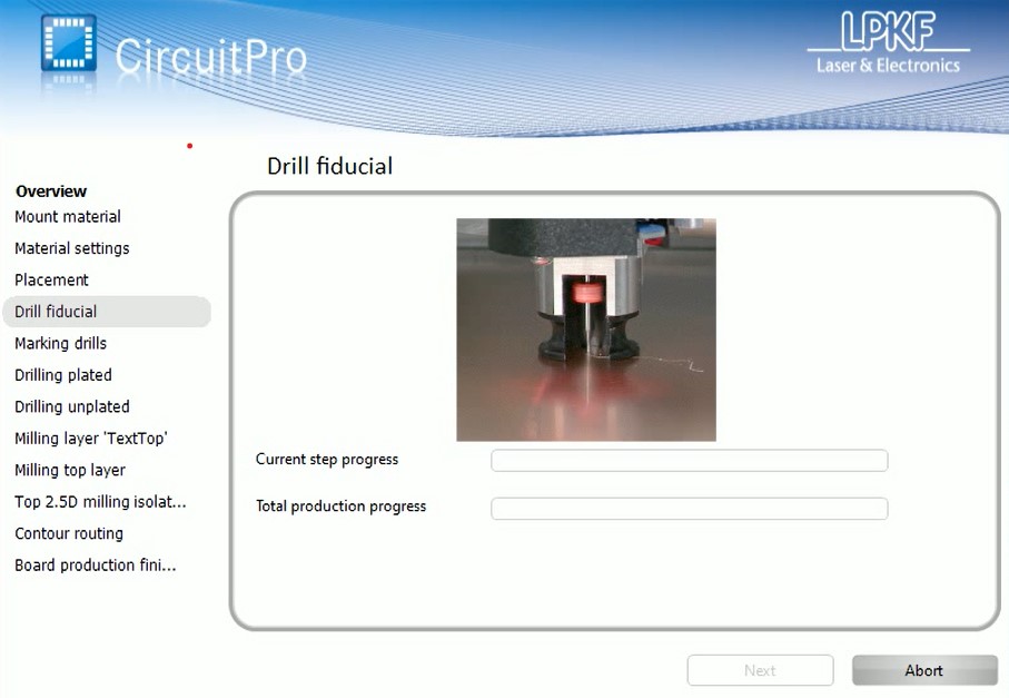
Step 10: Drill fiducials
Now the machine drills fiducials and also mentions which tool to mount for this action.
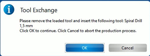
Accordingly we change the tool as shown below:
Step 11-14: Marking drills, drilling, milling top layer, etc
Just like the previous step, these few steps are about following the instructions and changing the tools appropriately as when asked for the specific action
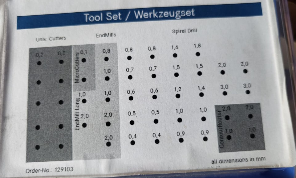
The stages and its tools used are listed below for single sided PCB (last iteration of mine) Step A: Fiducial hole marking
Tool: Spiral Drill 1.5mm
This step involves marking the end to end diagonal holes to define the boundary of the job
Step B: Marking
Tool: Micro cutter 0.1mm
This step involves the marking of all drill points, and crucial starting point for top layer milling
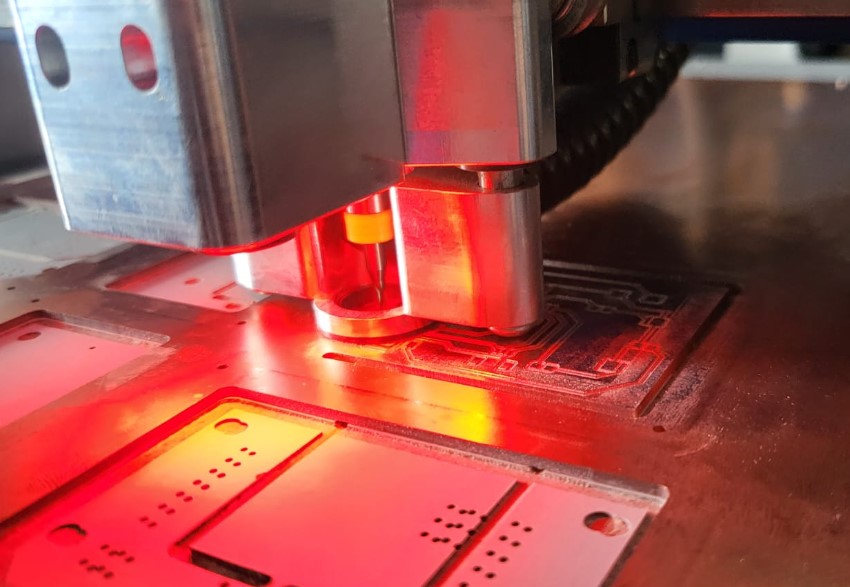
Step C: Milling
Tool: Universal cutter 0.2mmm
This step involves the actual milling of the 4 channels
Step D: Reference hole
Tool: Spiral Drill 2mmm
This is reference hole drilling to start the boundary cut
Step E: Boundary cut
Tool: Contour router 2mmm
This step is the last one to actually cut the outer boundary of the PCB
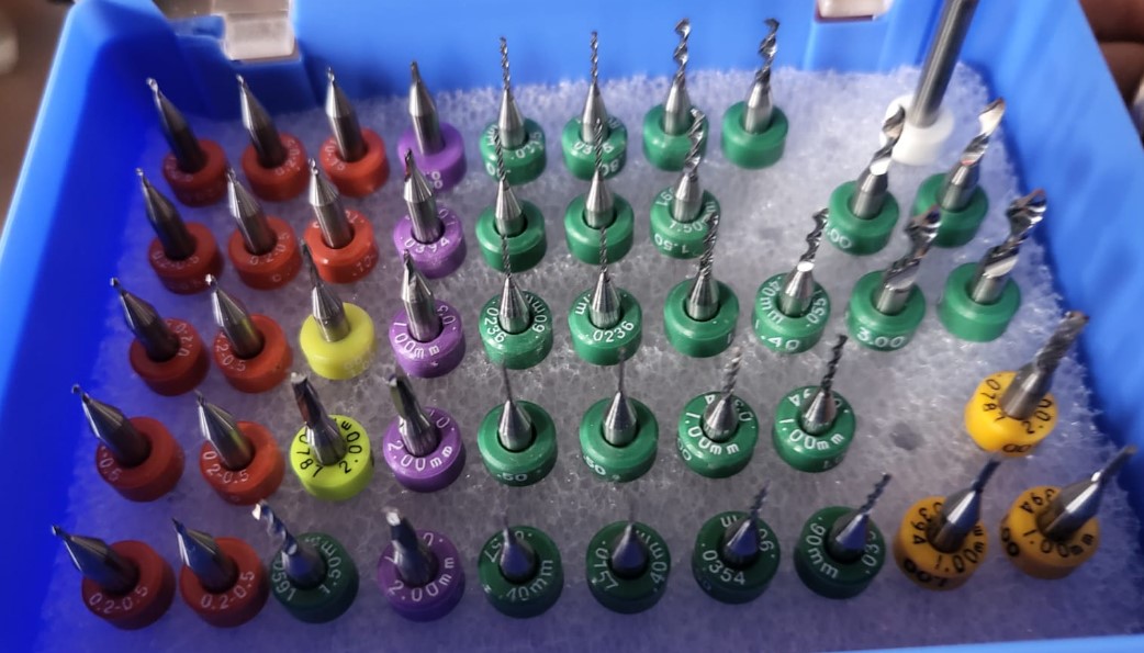
The extensive toolbox that comes with the machine has multiple tools as shown below:
Step 15: Final outcome Here's how the single sided PCB version looked like after successfull milling.
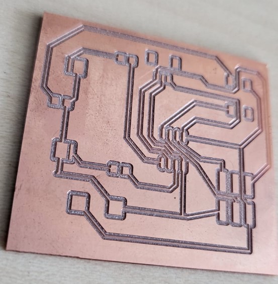
Here's how the previous failed designs looked like:
PCB design and production V2
So when the input devices and output devices assignment came in, I realised the convinience to use ATMega328p chip as it is the same microcontroller of that of Arduino Uno. So I did not actually continue with the previous board but designed a new one which I then also used for my other assignments.I have prepared the final PCB board which I am going to use for this assignment and also the other assignments like input devices. The board is same as the Arduino UNO Board because it has the same IC i.e. 328p, and does all the functionality of UNO.
I haven't included the in depth details of the PCB production for this as I have already explained that in depth for the previous versions. But in quick, the steps followed are as follows:
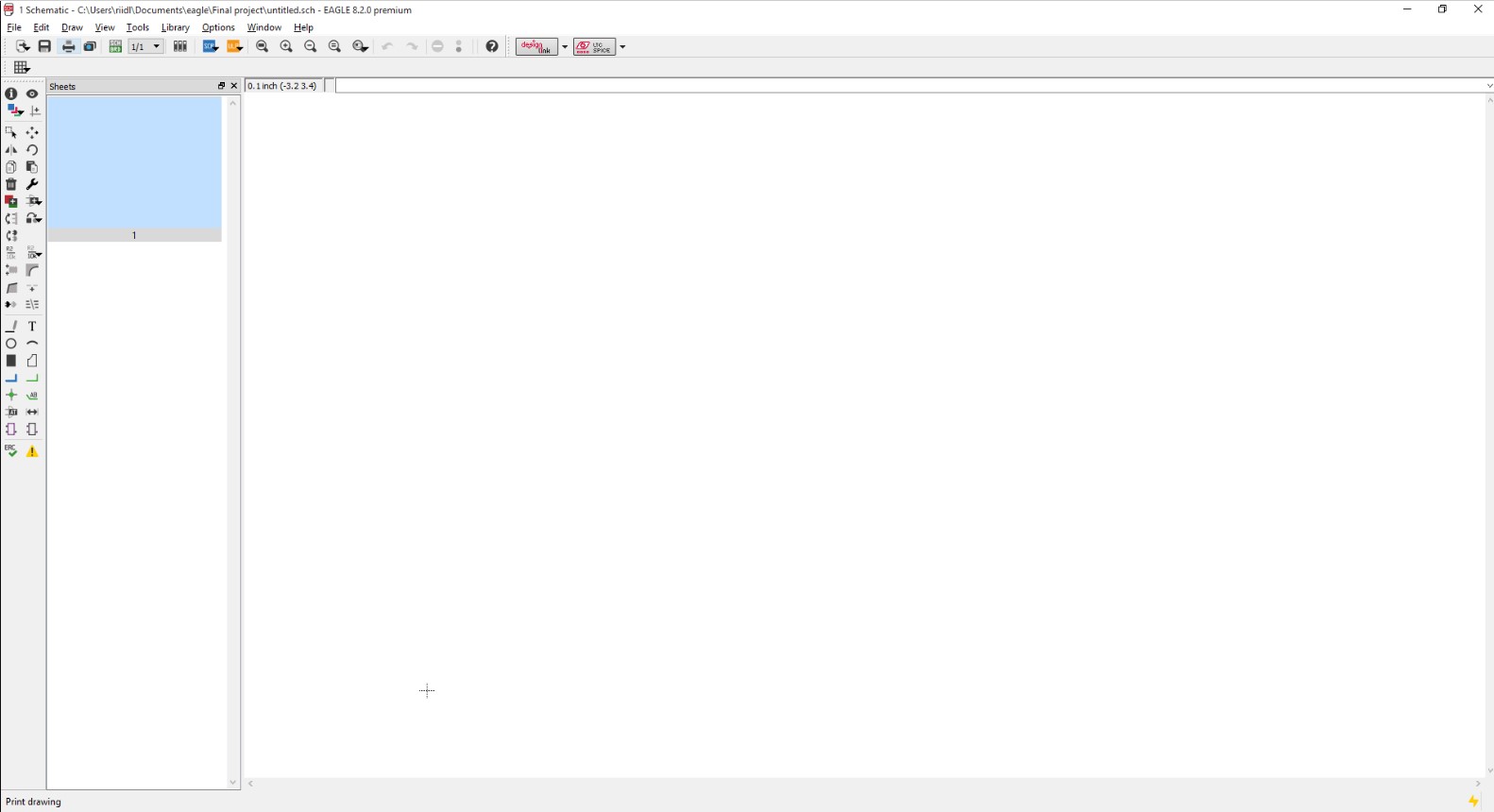
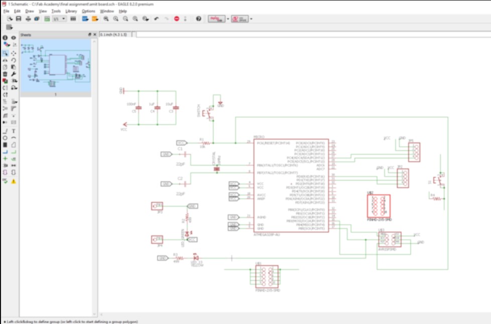
1. So I have used EasyEDA many times, and Neil mentioned to try new things out so I used Eagle Software for designing of my final PCB for this and couple of these input output device assignments. It was anyways also suggested by our regional guru during regional reviews taht i should try new things and not use the same software that I already know. So that is why I tried Eagle.
2. Use the ADD command to add the components to the design layout which is available under the command button bar.
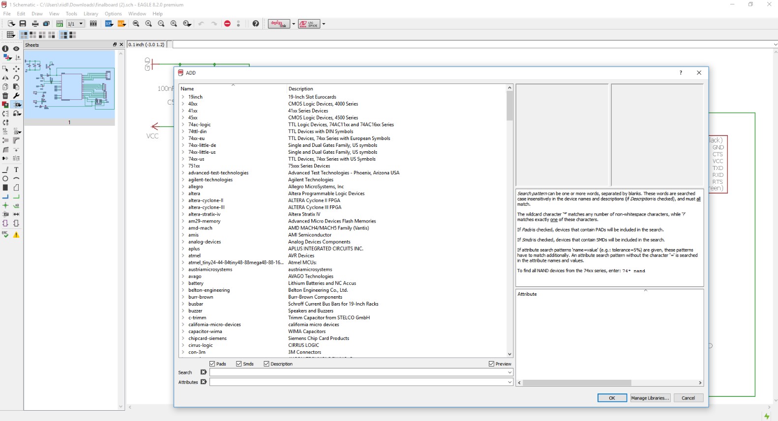
3. Add the atmega328p which is the arduino UNO chip.
4. Add all the components such as resistor, capacitor, Leds, button, AVRISP SMD header pins, etc.
5. Use the command net to join the two components pins with each other.
6. After connecting all the component with each other, to know whether all the components are connected or not with the ERC command.
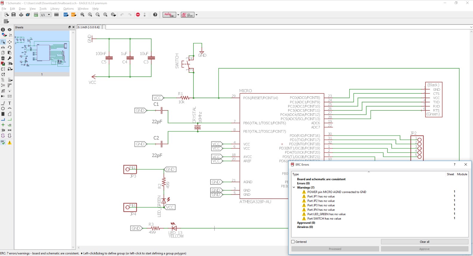
7. If there is no error from the ERC error dailaog box, we are ready to switch from the schematic file to board file.
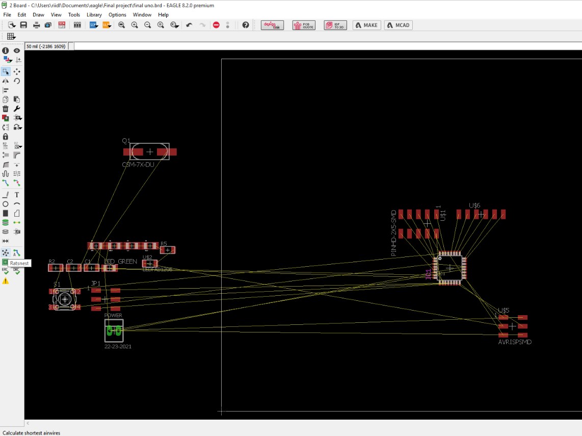
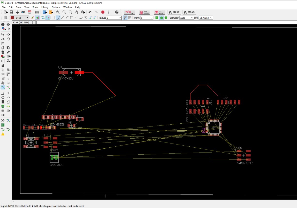
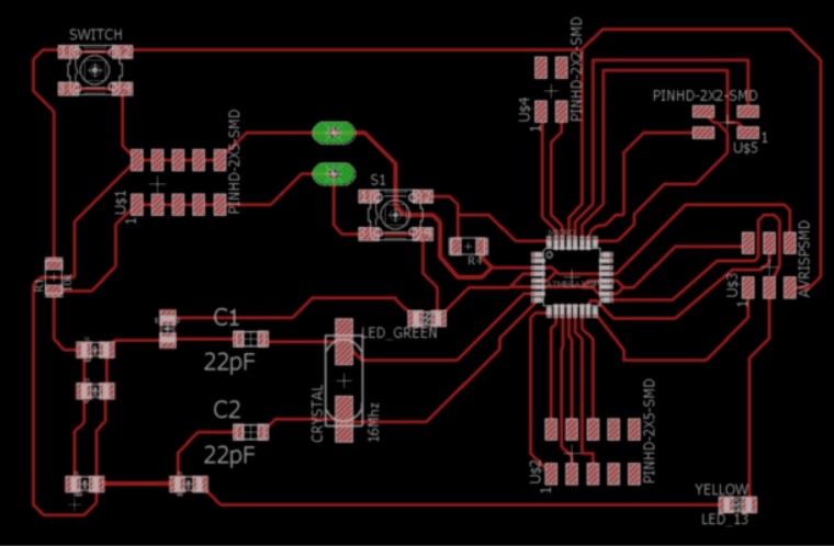
8. In the Board version, after arranging the components in the proper place, then route the wire with the routing option available from the command button bar. Before using the route option, select the ratsnet to so that the number of wires should be reduced.
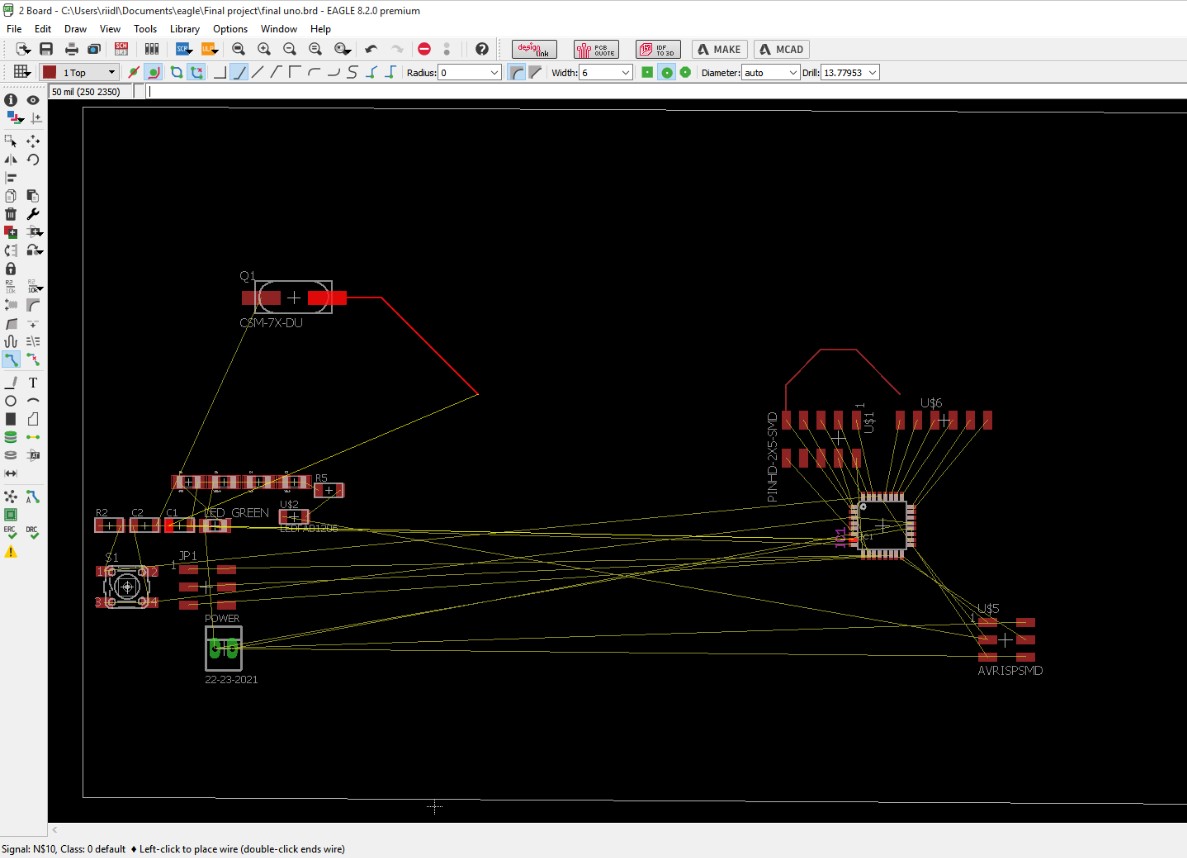
9. Then use the route option to make respective connections.
10. Then export the file for fabrication. Save it in .png format 600dpi monochrome.
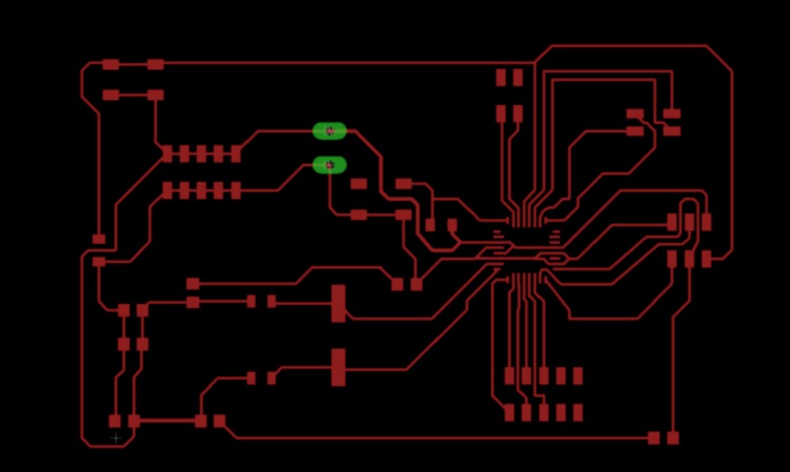
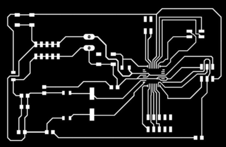
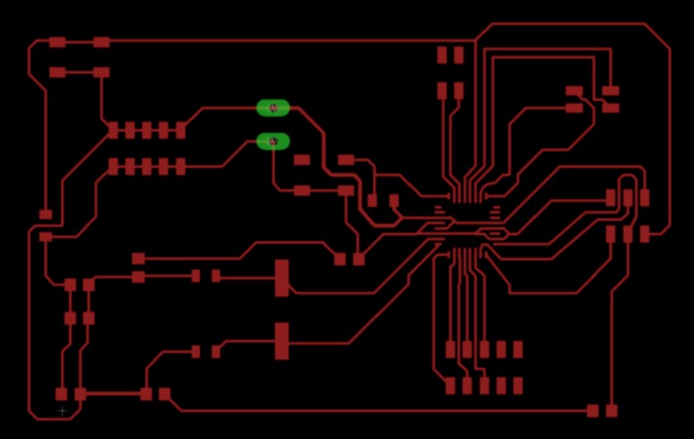
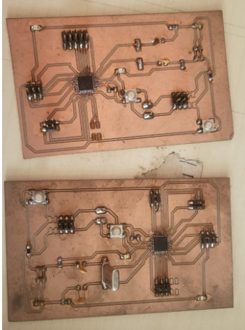
Below are the images of the final board:
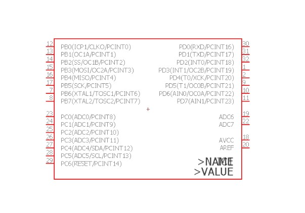
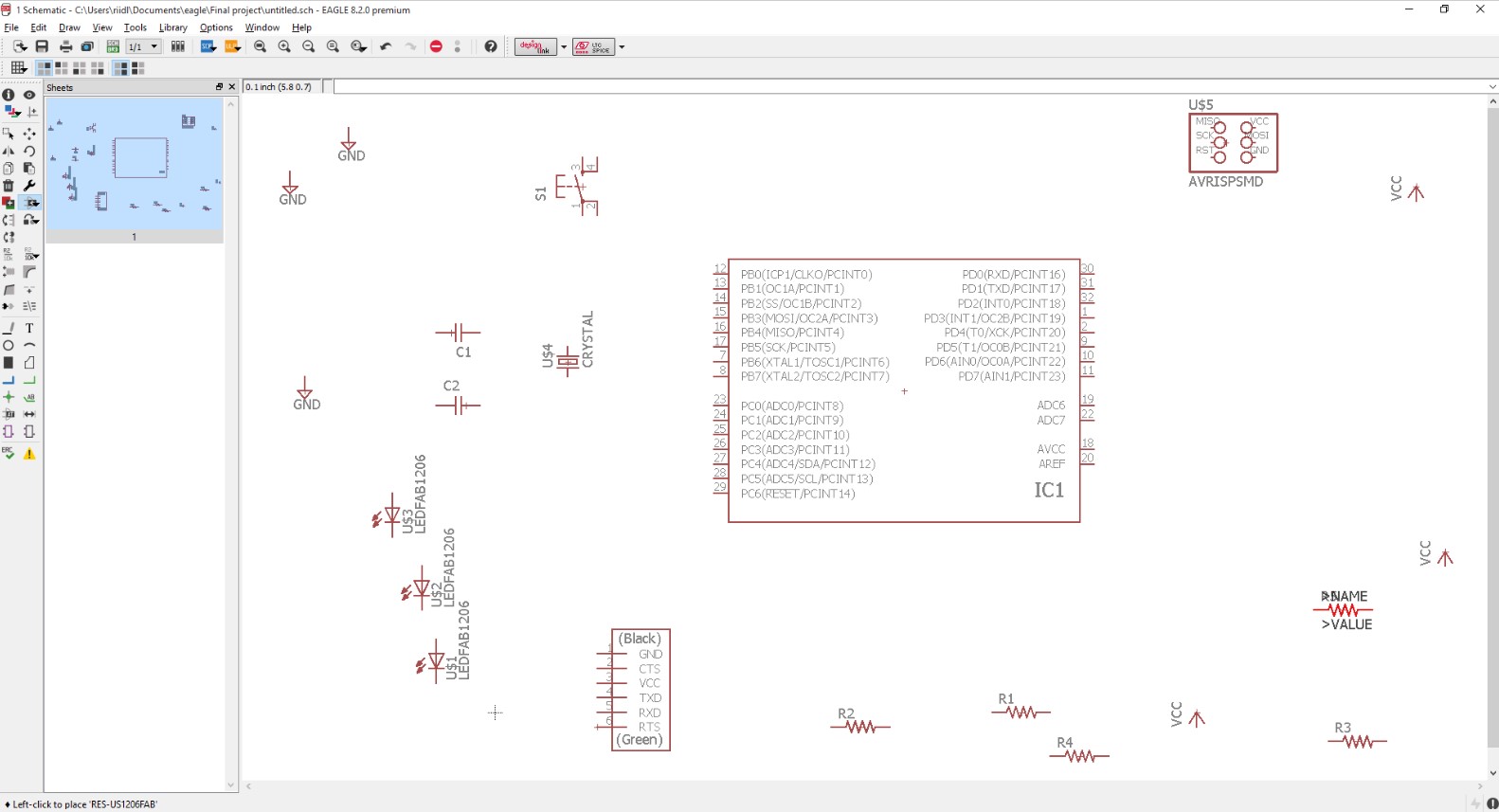
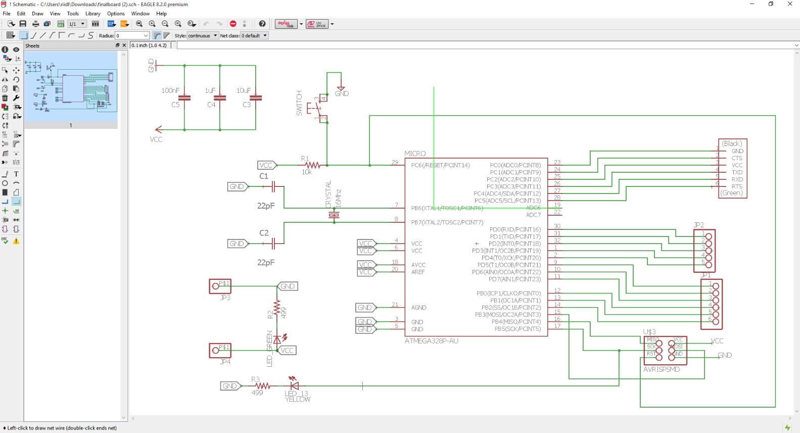
Schematic images of the board which was made in the Eagle software.
Board images of the final PCB.
PCB Soldering
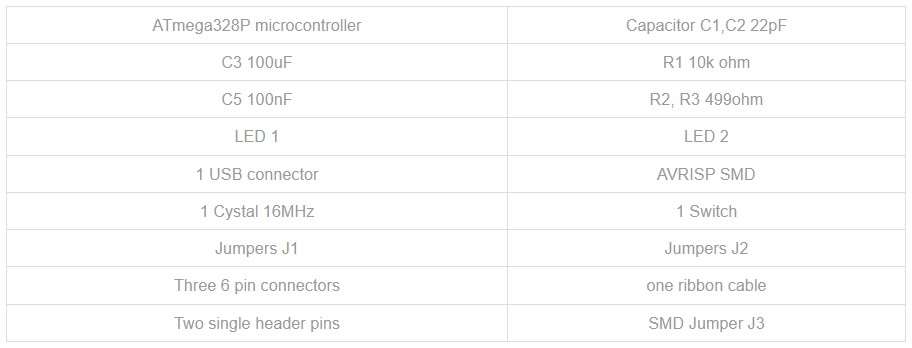
Next step up is PCB soldering. Before that we need to get all the components. All the electronic items I fetched from multiple electronics stores locally in Laminton rd, Mumbai.Components needed for the board:
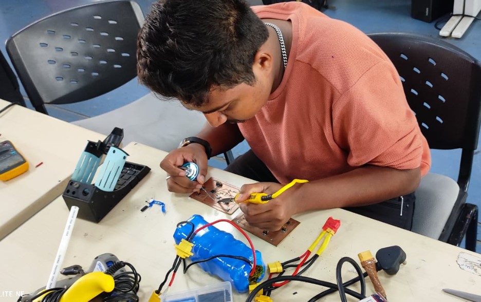
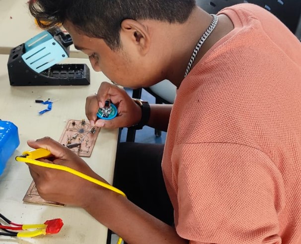
Once we have all the components, let's start soldering!
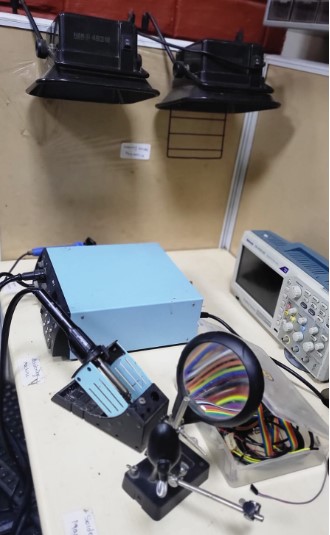
Step 01: Soldering station
Let's understand all the things you need ideally at your soldering station ofr a proper and safe soldering process.
Fume Extractor.
The fume extractor is responsible for sucking the air around the soldering area and filtering the air.
Soldering Station.
Silicone Work Mat.
Hot air gun.
Lamp with LED and magnifier.
Stainless Steel Anti Static Anti Magnetic Precision Tweezer Set.
Soldering tip.
Soldering station at riidl:
Soldering process:
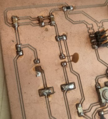
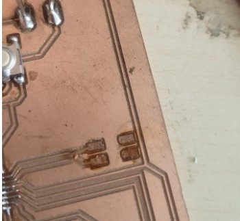
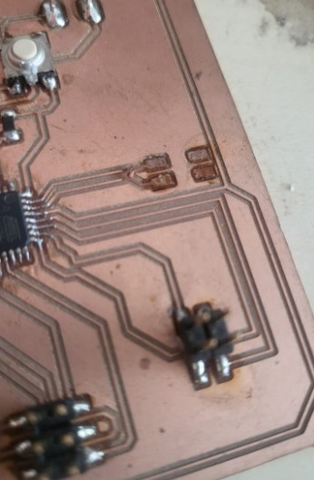
Images of the failed soldering attempts:
So I ended damaging some points of soldering during the soldering process and thus had to make the board all over again.
Learnings:
1. Don't over heat the gun - the solder doesn't stay down and comes back over the iron 2. Dont touch the solder reel directly to the gun - but the gun should touch the lead and the material to the board and the heat transfer should do the rest of the job 3. If anything goes wrong, don't try to resolve it by touching the soldering iron again, instead using desolder wick and/or desoldering gun and then after clearing all solder, resolder it. 4. Use a multimeter and test the connection after almost every solder if you are not confident.
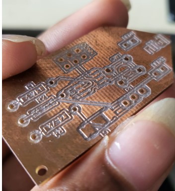
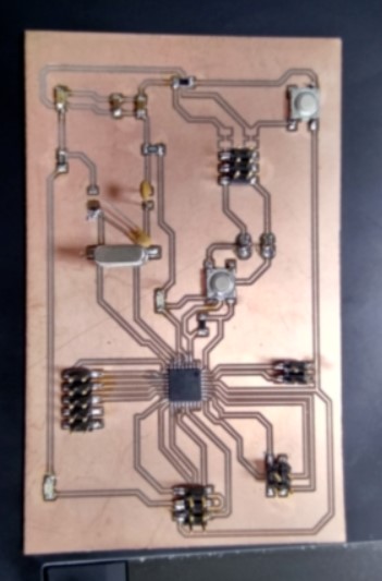
Image of the final working board after milled.
Testing the PCB
The PCB was tested by connecting it to the input and output devices. The same can be seen in detail in the specific week pages as linked below: Week 09: Output DevicesWeek 11: Input Devices
Download design files
Atmega328p fileGerber file Attiny 412
EasyEDA Attiny 412