6. Electronics Design
Electronics! My old enemy turned friend. Neil's session on the electronics design and especially the basics from V=IR, Capacitors, Resistors, Inductors, and some more like MOSFETs, Transistors and other components helped me revise my knowledge about electronics.For this week's assignment, we have to design a development board with an embedded microcontroller to interact and communicate with it. So basically, the development board we referred in the last week, for example, arduino uno is what we have to design on our own using an embedded microcontroller ie. ATmega238p for the case of Arduino Uno. Before we go into the process of designing the development board, let's first understand some basics of electronics.
Understanding the basics of electronics
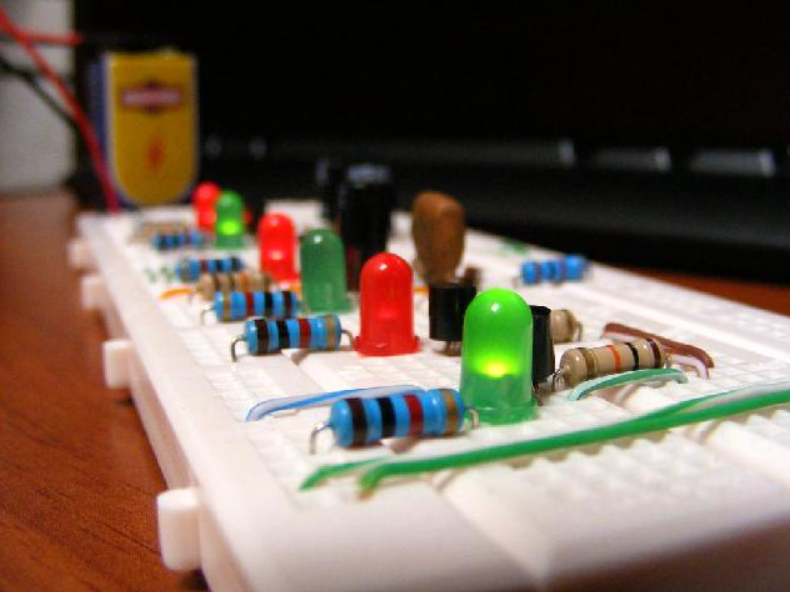
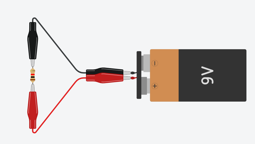
What is an electronic circuit?An electronic circuit is composed of individual electronic components, such as resistors, transistors, capacitors, inductors and diodes, connected by conductive wires or traces through which electric current can flow. A complete circuit can be as simple as a battery and a resistor as shown. If the resistor is missing then the battery would short circuit and drain.
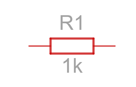
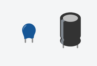
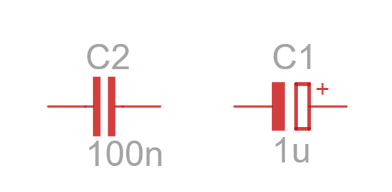
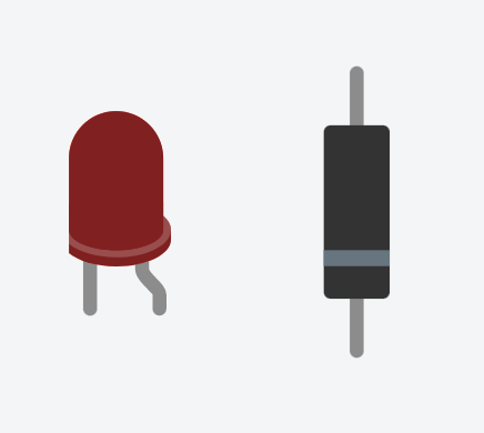
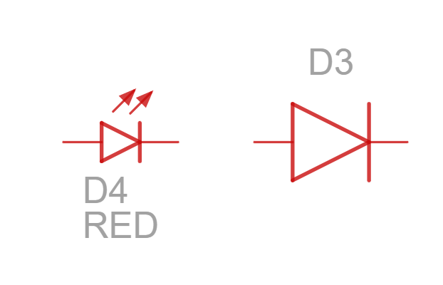
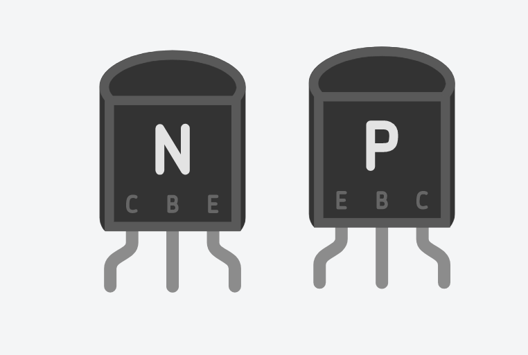
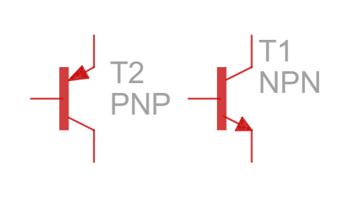
Electronic components, its symbols and basic functions
To understand circuits better, let's know more about the electronic components
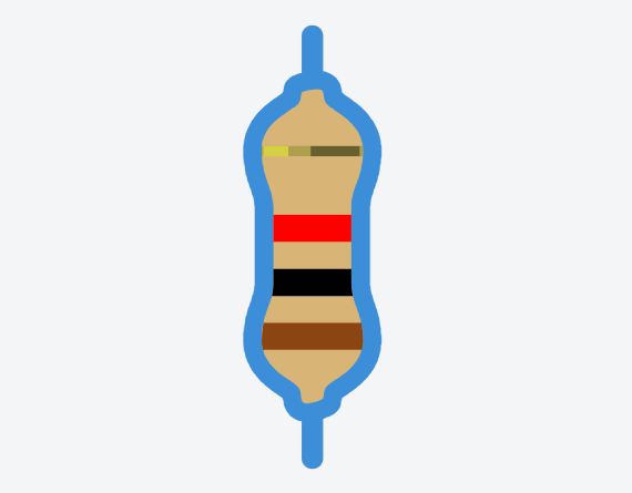
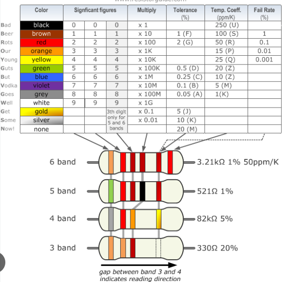
The color coding of resistors is as follows:
Designing a development board with an embedded microcontroller
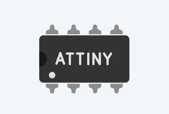
So for this week's assignment, I am going to use ATtiny412. ATtiny412 is a microcontroller from the Atmel AVR family of microcontrollers. It is a low-power, high-performance 8-bit microcontroller that is designed for a wide range of applications, including industrial, commercial, and consumer products. The datasheet of ATtiny412 can be found here: ATtiny412 Datasheet The block diagram of ATtiny412 is as follows: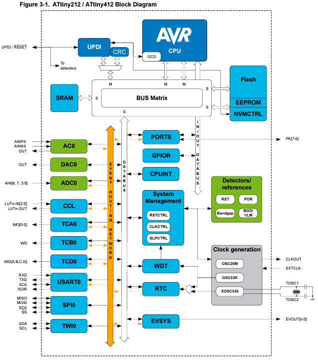
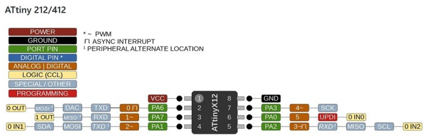
The pinout configuration is as shown below:
Understanding ATtiny412
So for the assignment, we decided to use ATtiny412 as the embedded microcontroller to design our development board to communicate and interact with. At first, it was a bit scary as I had no idea what to do next! But I came across some documentations from other students and past fabacademy projects that helped me understand better.Starting with understanding the pins on ATtiny412,
PIN 1: Vcc
Vcc is the power supply pin.
PIN 2: TXD
Transmit Data, which is a signal line used to transmit data from one device to another in a serial communication protocol
PIN 3: RXD
Receive Data, which is a signal line used to receive data from another device in a serial communication protocol
PIN 4: SDA
Serial Data Address, which is a signal line used in the I2C (Inter-Integrated Circuit) communication protocol to transmit data between the master and the slave devices
PIN 5: SCL
Serial Clock, which is a signal line used in the I2C (Inter-Integrated Circuit) communication protocol to transmit clock signals from the master device to the slave device
PIN 6: UPDI
To communicate with ATtiny412, we have UPDI pin.
Now what is UPDI?
UPDI (Unified Program and Debug Interface) is a communication interface that is used to program and debug microcontrollers produced by Atmel (now part of Microchip Technology). UPDI is a two-wire interface that is used to communicate between a programming device (such as a debugger or programmer) and a microcontroller
PIN 7: SCK
Serial Clock, which is a signal line used in various serial communication protocols such as SPI (Serial Peripheral Interface) and I2C (Inter-Integrated Circuit) to synchronize the data transmission between the master and the slave device
PIN 8: GND
GND is the ground pin.
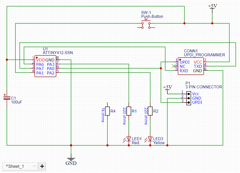
The circuit design using ATtiny412 needs to have a resistor, a LED (output device), a switch/button (input device), a power unit, and ofcourse conducting wires.
Understanding the PCB design softwares
PCB design can be done on multiple softwares such as EasyEDA, Autodesk Eagle, KiCAD, etc. The first time I have worked on designing a PCB was in the Autodesk Eagle. But the UI of the software was not something I got acquianted to and thus shifted to the EasyEda software. Another benefit of the EasyEda software is that you can directly order the PCBs for printing/mass printing from the JLCPCB. The first interface of the EasyEda looks like the photo below as shown.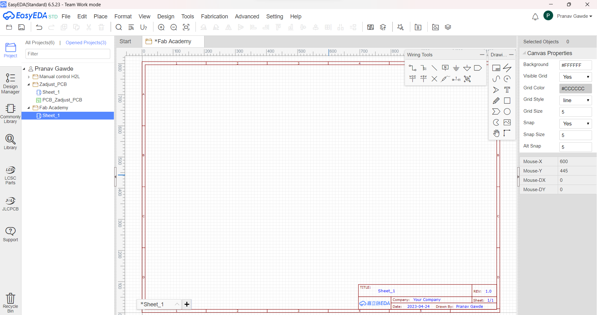
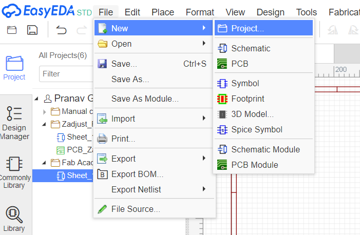
To start designing, FIle > New > Project. Then initiate a new schematic to start first.
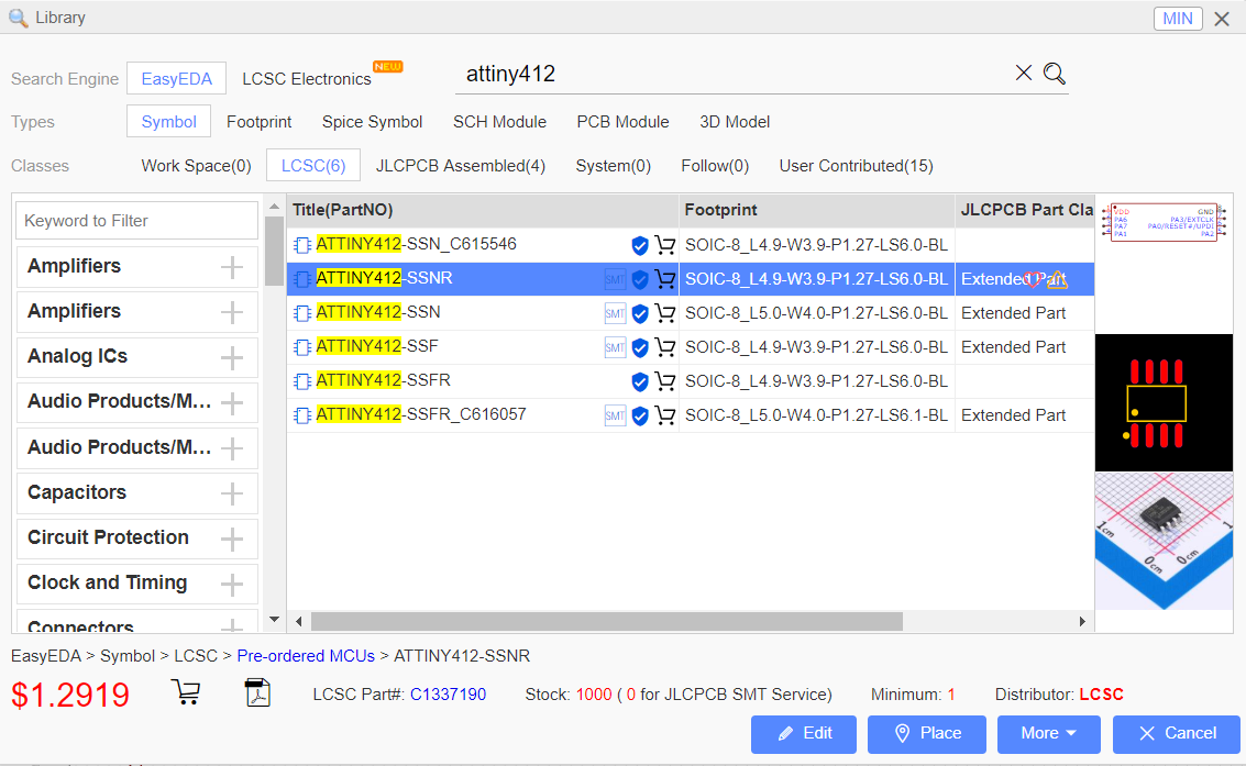
To start importing electronic components, open the library panel and enter the name in the search window as shown in the figure below:
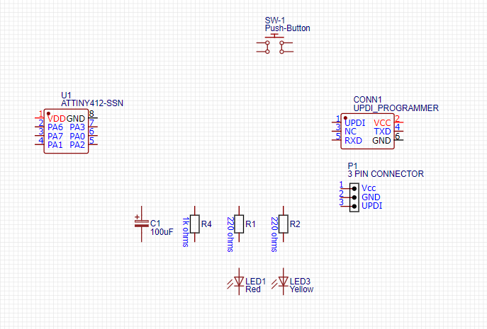
I referred to a ATtiny basic circuit example online and started importing components accordingly from the library.
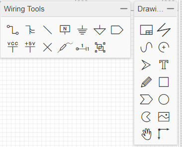
Once I imported all the necessary components, it was time to connect the wires in the schematic. You can do that using the top right panel in the interface as shown in the figure below:
Tip: Make sure to mark x on the ports that are not going to be connected to anything or it will show as an error.
After all connections are made it looks like this:
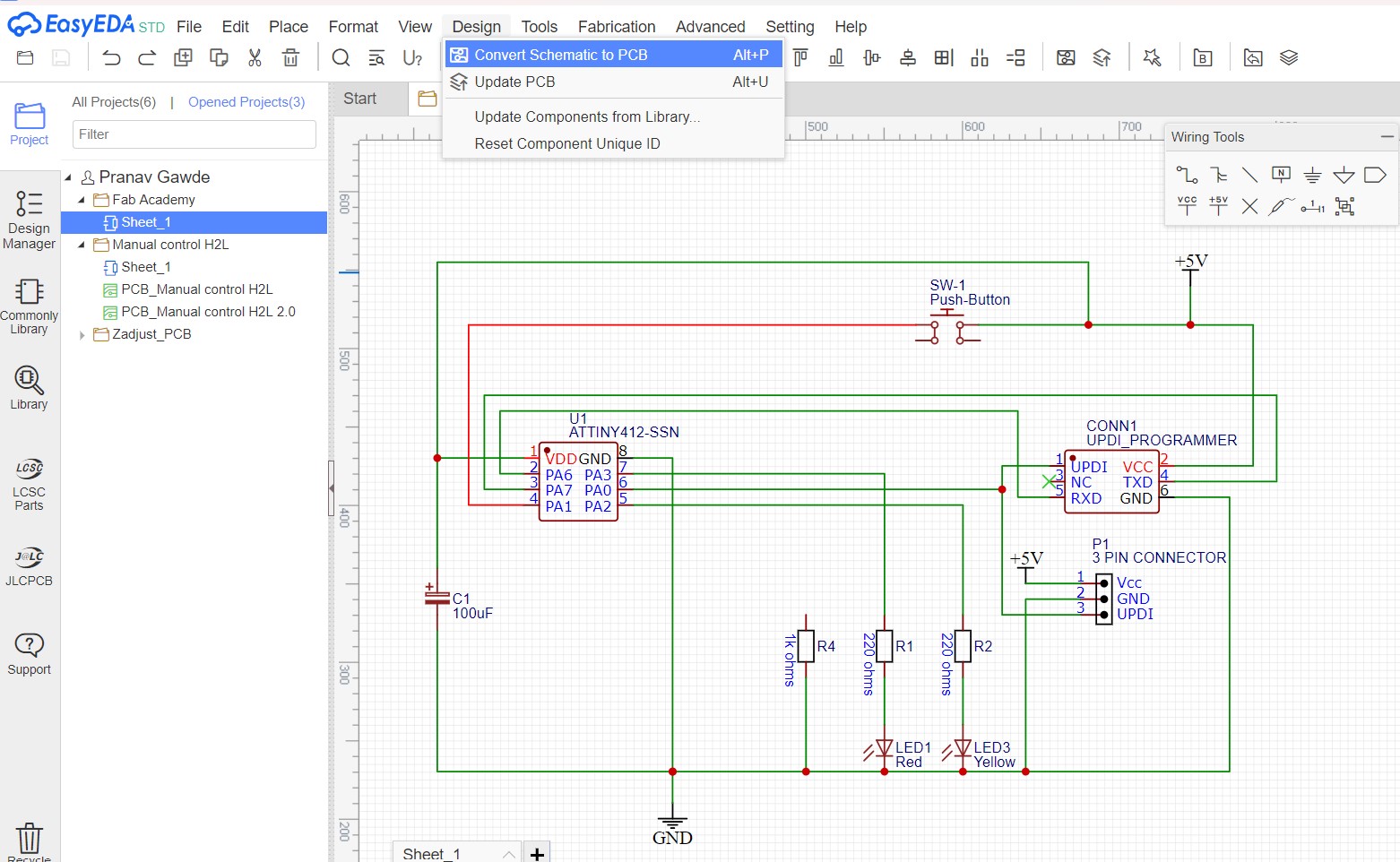
Once all the connections are done, we conver the schematic into PCB design. The steps are Design > Convert schematic to PCB or shortcut (Cntrl+P)
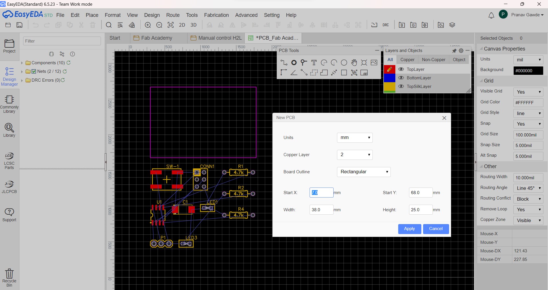
You can check nets before converting when the dialog box pops up. Once that is done, the following PCB design dialogbox opens to choose the parameters. You can keep to default parameters as EasyEDA sets right parameters anywhich ways.
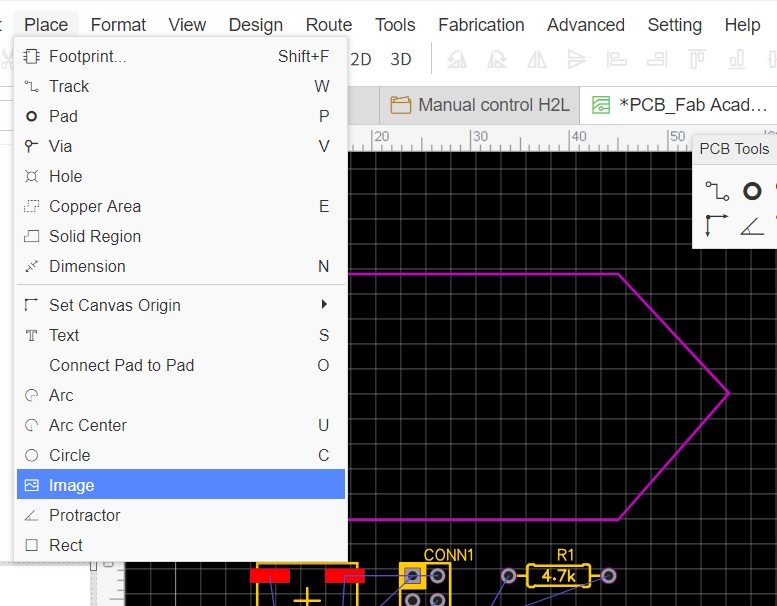
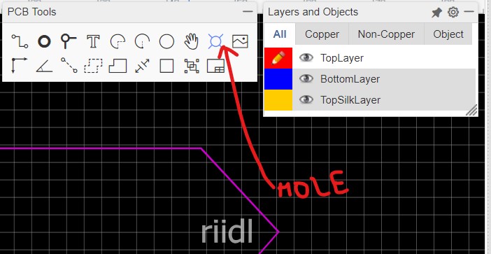
Now first we need to move all the components to the desired locations on the board. The standard board shape from the software is a rectangle as seen above. But we can design whatever shape we want and can also add images or logos to the PCB.
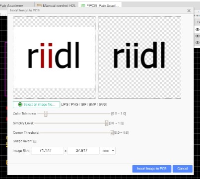
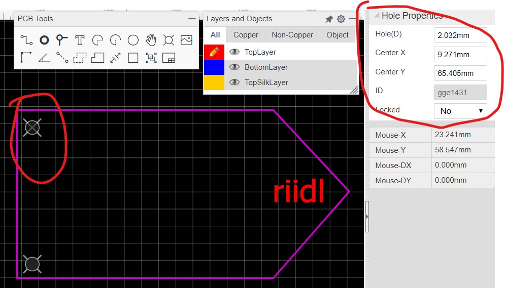
For mounting purpose of our PCB, we can add holes and also edit the size, etc as shown below:
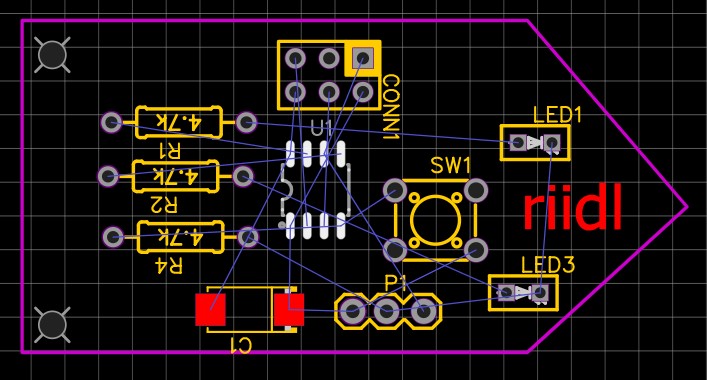
Now next step is to arrange the components in the desired positions on the board and then route the wiring.
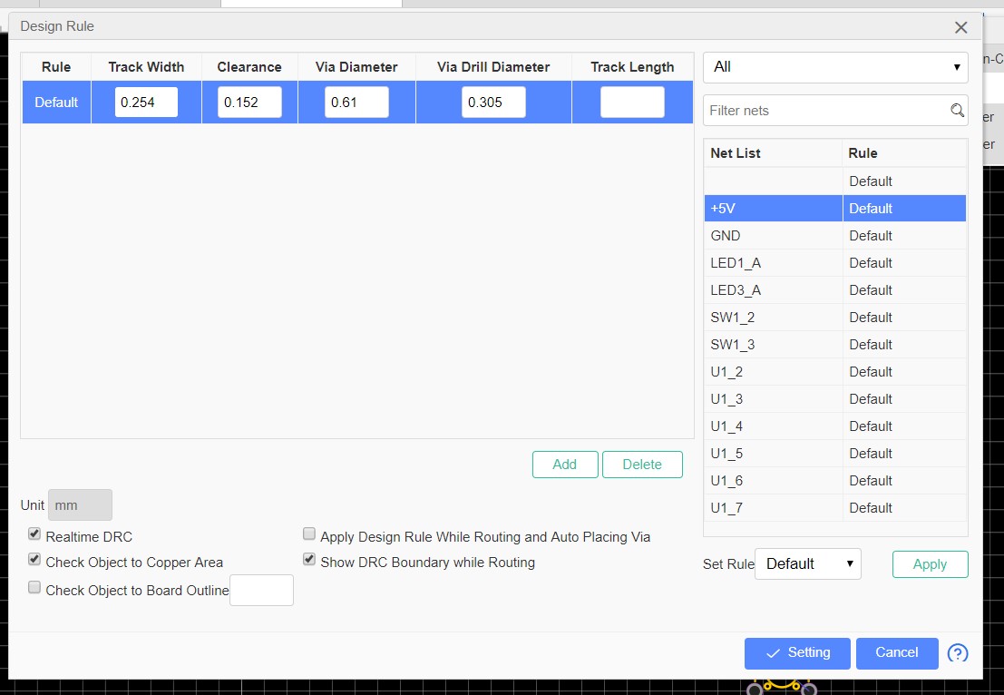
For routing the connections, we need to know the design rules for the same. Here's the dialog box and the settings you should ideally use.
Design > Design rules > Setting
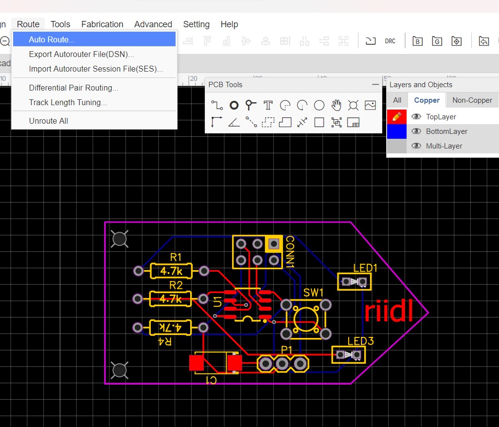
Actually, ideally for a ground connection, you should just have a plane, but since this is just 5V circuit and a simple one, 0254mm width ground line should also be fine. While you can manually connect using the wiring option, there is a auto route option in EasyEDA as shown in the figures below:
ROute > Autoroute > Run
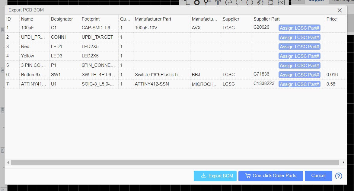
EasyEDA also generates BOM that can be used to order the components quickly or if we are ordering the PCB directly from the JLCPCB, then check for availability.
Fabrication > BOM > Export BOM
Next step is to do DRC check that is Design rules Check from the software end. It is very important to do this before you export your Gerber files. If we have any node open, or any connection incomplete, this check points out those mistakes.
Design > Check DRC
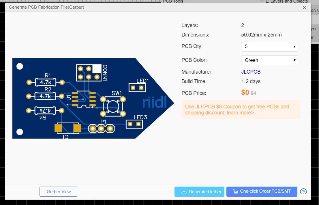
Last step is to download Gerber files, which are needed in the next software for PCB milling.
Fabrication > PCB Fabrication file Gerber > Check DRC > Generate Gerber
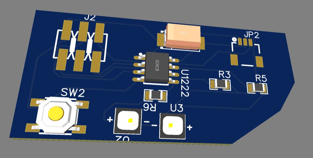
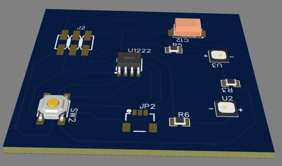
In EasyEDA, you can also visualise the 3D view of your PCB after assembly, provided you have chosen the right components from the library back during the schematic design time and those components had a 3D view uploaded in the library.
Just click on the 3D option in the top toolbar. So these below are the 3D views of the 2nd and 3rd iterations of the PCB.
Exploring TinkerCAD
The initial test look of your circuit can be done on TinkerCAD. TinkerCAD is a free web app for 3D design, electronics, and coding. Once you sign up with your email id, the interface looks as shown. As seen in the image below, you can start creating your design by clicking on the create option in your designs section.
You can start designing your circuit by simply searching and picking and dragging the components from the right panel into the central wrkspace area
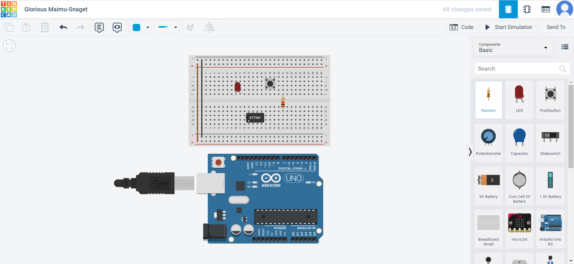
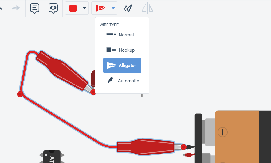
To route wiring for the components, you can choose color and type of the wire connection from the top panel as shown:
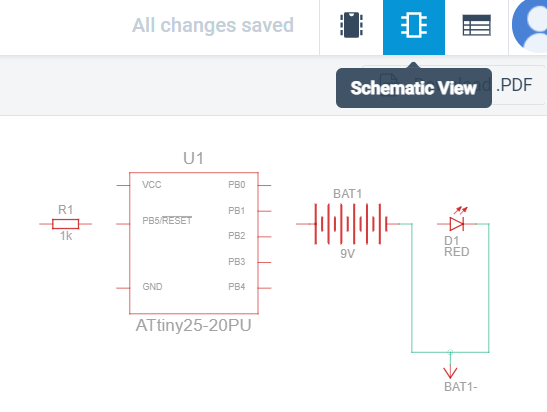
You can view the schematic view by choosing the top right corner schematic option as shown below. Here you can edit the circuit design based on the schematic and check if any wiring is wrong or a connection is left to be done.
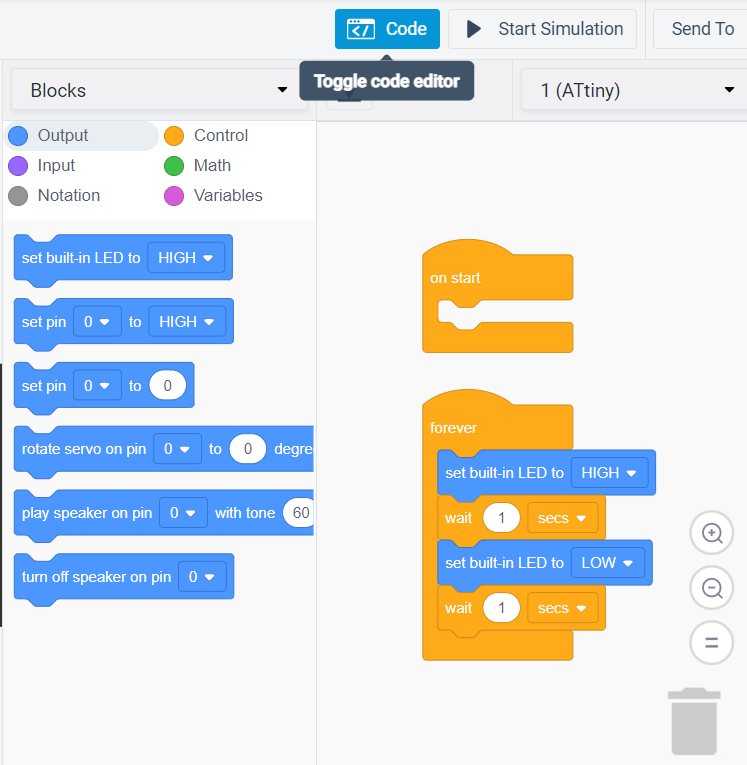
You can also code microcontrollers in tinkerCAD using the Code editor option on the right as shown below:
I just tried TinkerCAD to explore the software and see its possibities. It is overall a very good software to experiment and simulate your designs. But to actually make one, I will move back to proper design softwares for PCBs.
Download design files
Attiny412 EasyEDA zipGerber file PCb zip