Week_08: Electronics Production
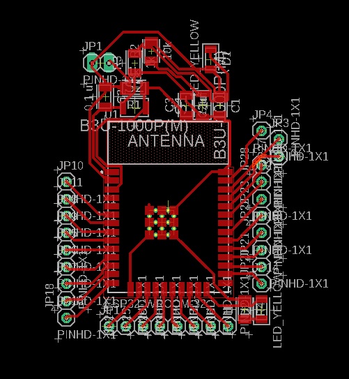
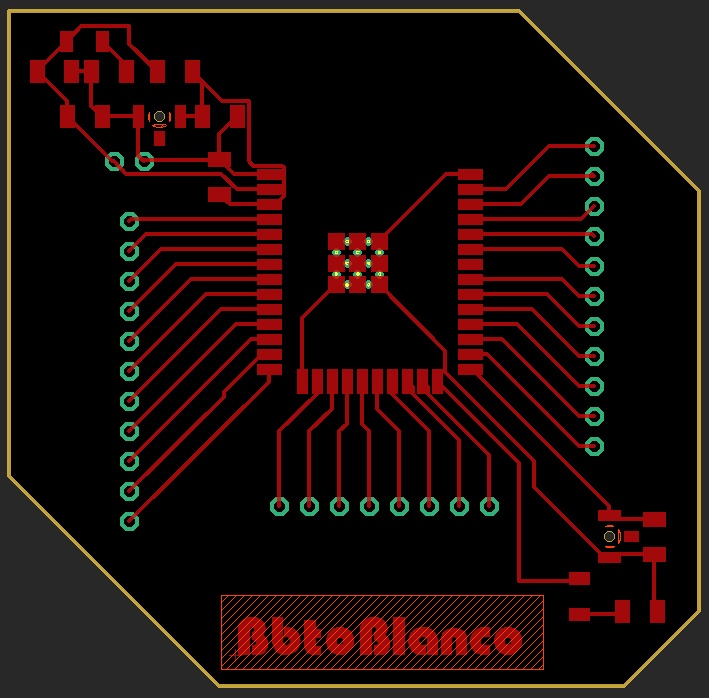
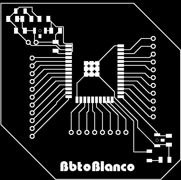
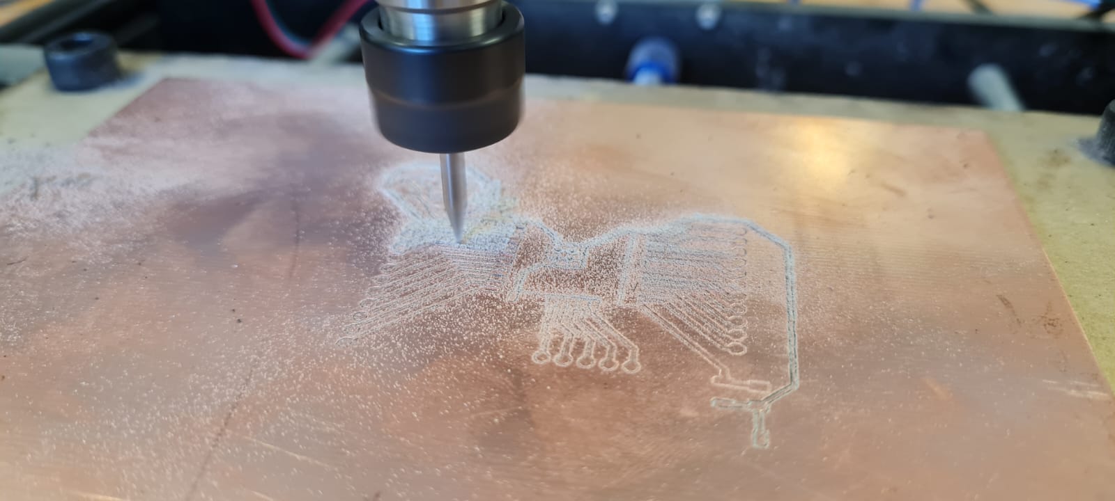
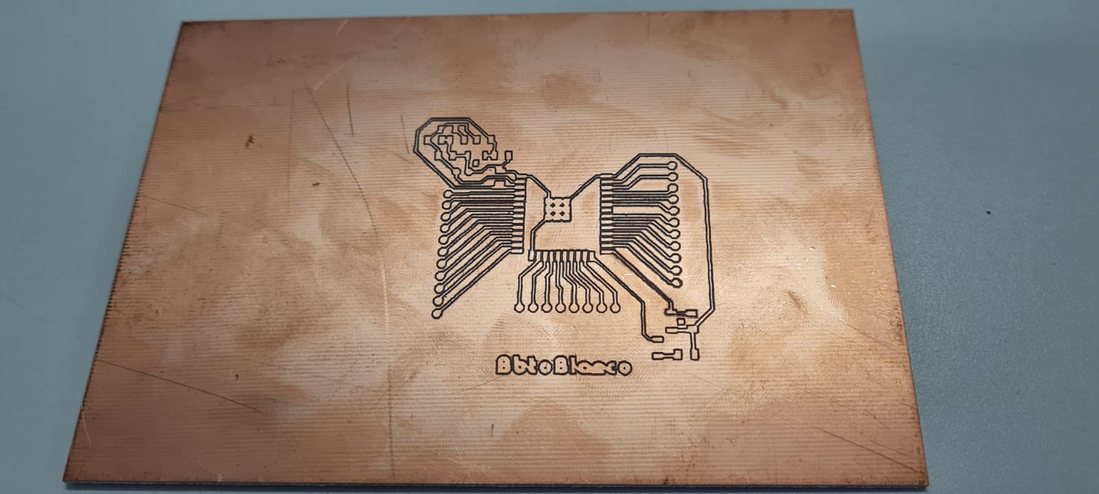
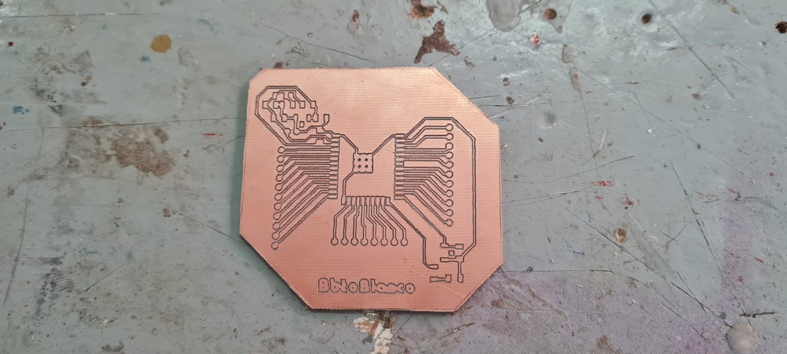
This week's assignment is about materializing the circuit board for our final project, which was "designed" on Week_06: Electroincs Design. This is done through a process of first having the final design of the Printed Circuit Board and circuit, then transfering it to a 3D model, then to a high resolution *.png* image that can be interpreted with the online software Mods, which converts the data into gcode for a machine to mill the paths, connections and holes into a copper plate. After having this piece machined, one can solder the components for the circuit and Voilá! Of course the theory is kind of easy. The milling on the copper plate is a method chosen because of its relatively low impact and difficulty, as most of the other processes utilize acids and toxic chemicals to remove the copper on certain places. Another interesting alternative is using the Vinyl Cutter, with a special kind of vinyl that has a copper lining, in which one cuts the paths and connections, for later appliance on (almost) any surface, like plywood, acrylic or even some fabrics. Unfortuantely I couldn't find such vinyl so it was necessary to learn to use the Minimill, a machine quite similar to the one used on Week_07: Computer Controlled Machining, but in a much smaller scale. First things first, I had to repeat the design for the PCB as I forgot about one connection, that apparently was very important. I repeated the process for converting the circuit schematic into a functioning PCB (Right image).
Design Rules
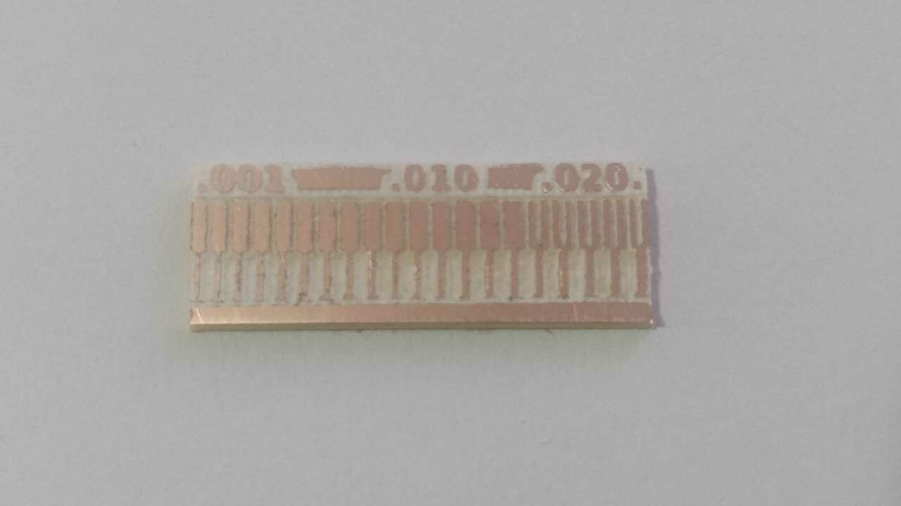
The term Design Rules means the standarized shapes and thickness of the paths, the size of the different components, and the way they are connected to the board. This specific design had the next Design rules:- Most of the capacitors are size: 0805, which means that the size of the component is .08in x .05in as this were the ones available on the lab.
- The resistors, the LEDs and one capacitor are size: 1206 meaining that the component is .12in x .06in as this are the most easy to solder SMD components.
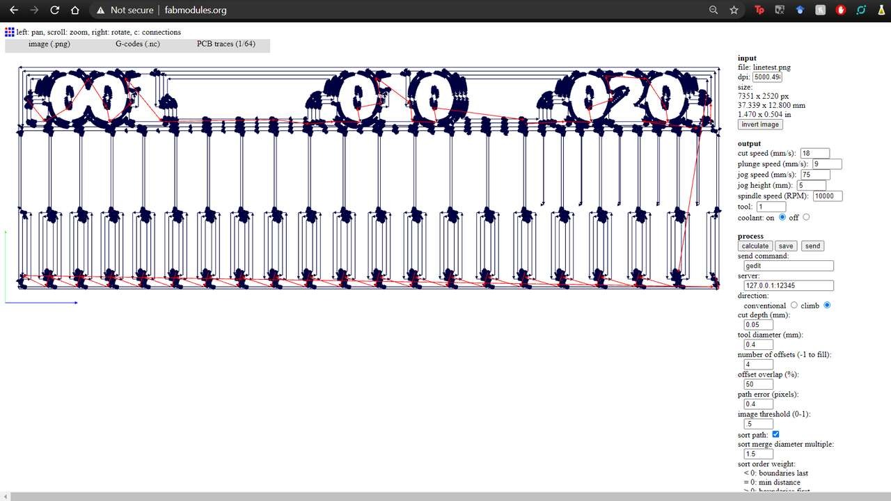
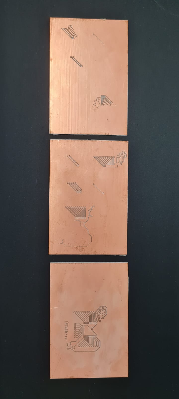
- The thickness of the electric paths is .2in I got this number from several (18) tries and errors. The first one I tried was .016in and the minimill completely destroyed the paths as the milling bit was to big for this.
- The size of the soldering base for the components depended entirely on the component size, for example the pins have a standard .06in base, and the 1206 components' base measures .05in x .1in
The next step is to transfer this abstract image of all the connections and components into an understandable image for the post-processor software. This is done by blocking out the layers that I didn't want to be on the final PCB, such as names, values and characteristics of the components. Then using the command line on Fusion 360 for exporting the image into a *.png* with the highest resolution, in this case I used 300 dpi.
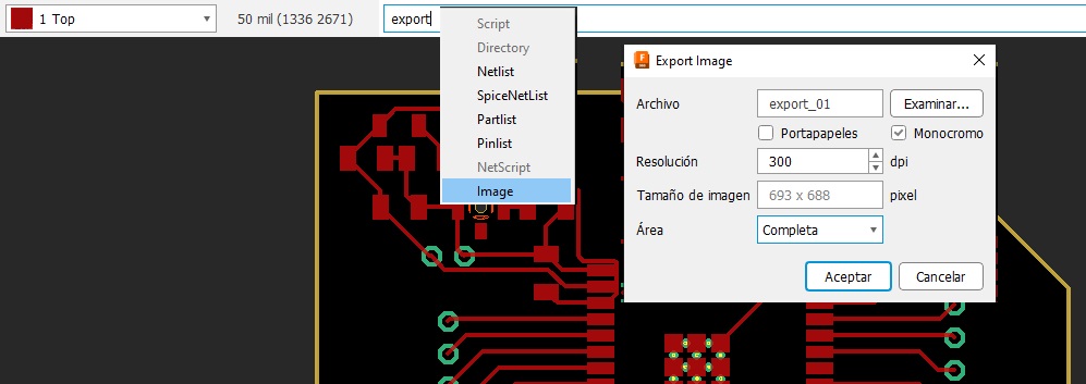
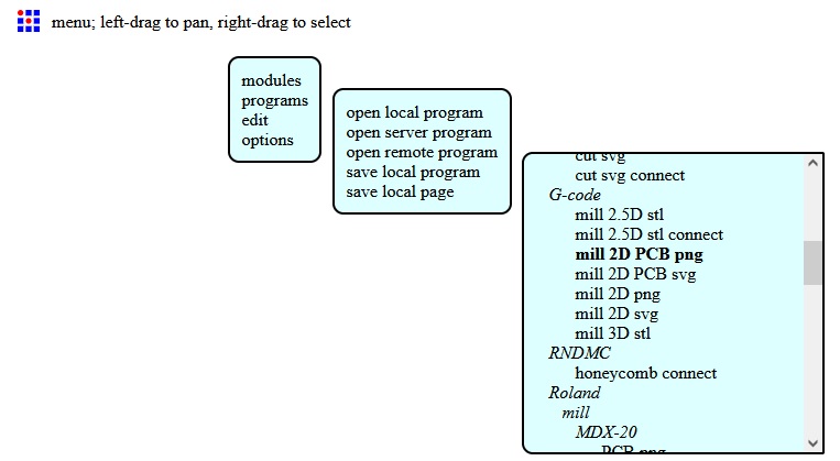
Having an awesome PCB, it was time to go to Mods, the online software developed by amazing people at the FabFoundation for a lot of different applications. This program works by having different inputs like images and vector files, and translating them into a language that the machines can understand and execute, like 3D printers or Milling machines. The interface is minimal so it was a bit hard to understand at the beginning, but with a bit of help (and some time) I was able to formulate a simple workflow. It starts by right-clicking the screen, then going to the
programs title, selecting the Open server program and then selecting the mill 2D PCB png. This will
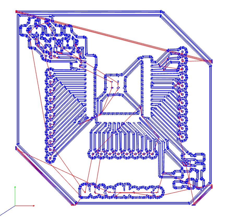
Now we must import the "Circuit board.png" file into
mods and add the values for our cutter diameter, feed speed of the machine, determine which are paths and which are holes, etc. We now click the button Calculate and the program does its magic, by outputing a gcode that can be used with most minimilling machines.
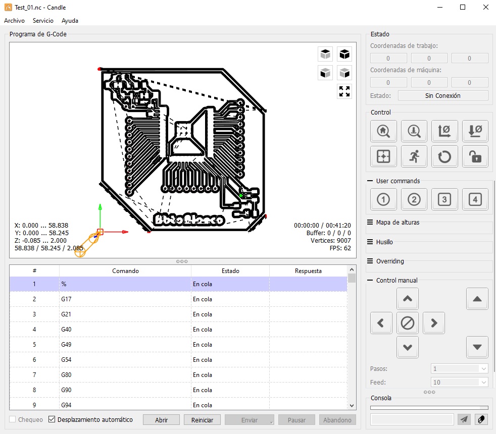
 This text file is now oppened on a post-processor which can control the machine, in this case it's an open-source software called Candle, which is a visual interface that communicates with the machine and tells it what to do.
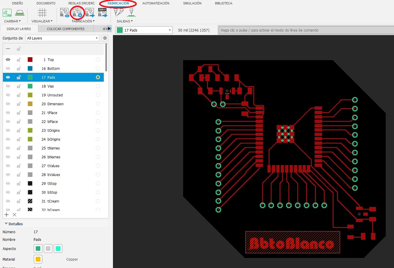
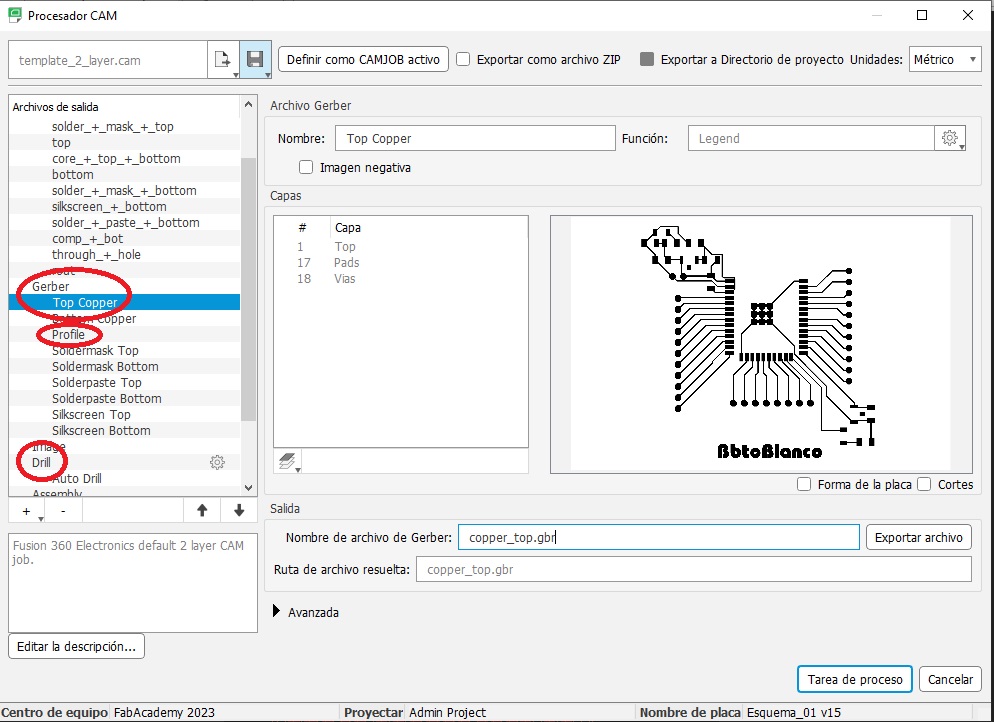
 The rest is waiting for everything to be programmed perfectly... and it didn't. I commited the mistake of only exporting one file, and when trying the Mods platform to correct that, it appeared to be down. So the next step was repeating the export process but this time not as *.png* images but as *.gbr* files. This
is done through a similar process, by using the
The rest is waiting for everything to be programmed perfectly... and it didn't. I commited the mistake of only exporting one file, and when trying the Mods platform to correct that, it appeared to be down. So the next step was repeating the export process but this time not as *.png* images but as *.gbr* files. This
is done through a similar process, by using the fabrication tab on fusion 360 and the CAM Processor tool. The layers that need to be exported are Top Copper, Profile and Drill. Each on a different file.
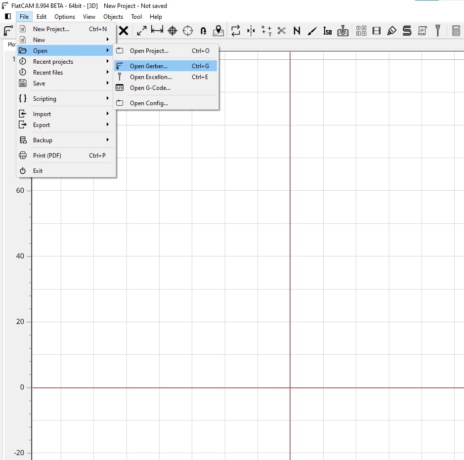
Afterwards I used a software called FlatCAM, which converts the file into gcode for the machine to cut the PCB routes. We start by importing the *.gbr* file into the software, then giving them the propper values for feed rate, spindle speed, tool diameter, etc.
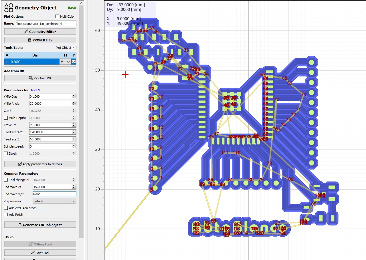
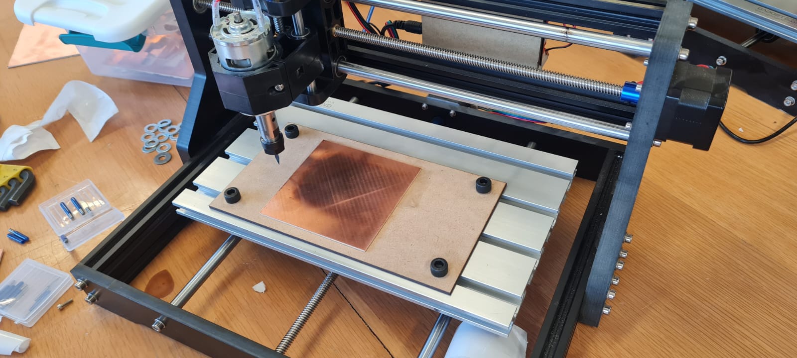
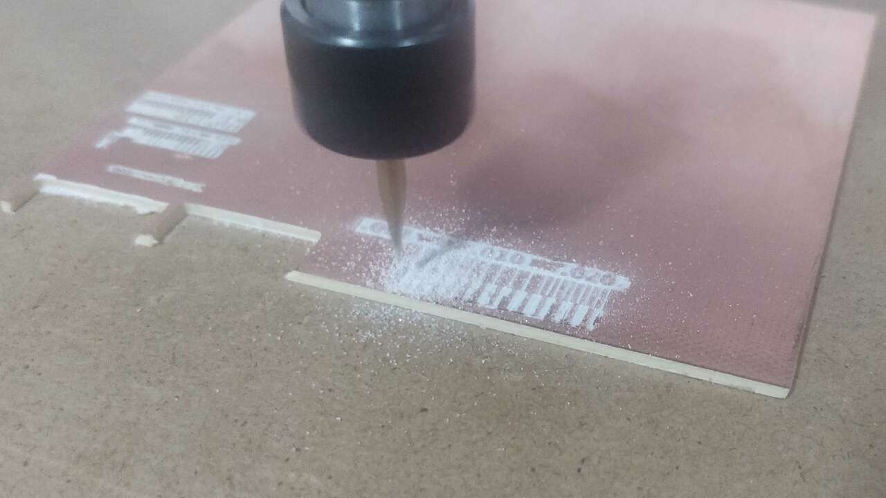
The Milling Machine
The machine is a 3-axis with a 15W spindle that goes around 16,000 RPM. It uses the GRBL firmware and was controlled through Candle software. On this test we determined which was the best size for the paths and components (I wish I had done that before starting but this learning curve has been very useful). The motors used on this machine are NEMA 23 which can produce up to 1.26 Nm torque and work with 12V 2.8A, very powerful for breaking the resistance of the cutting tool.
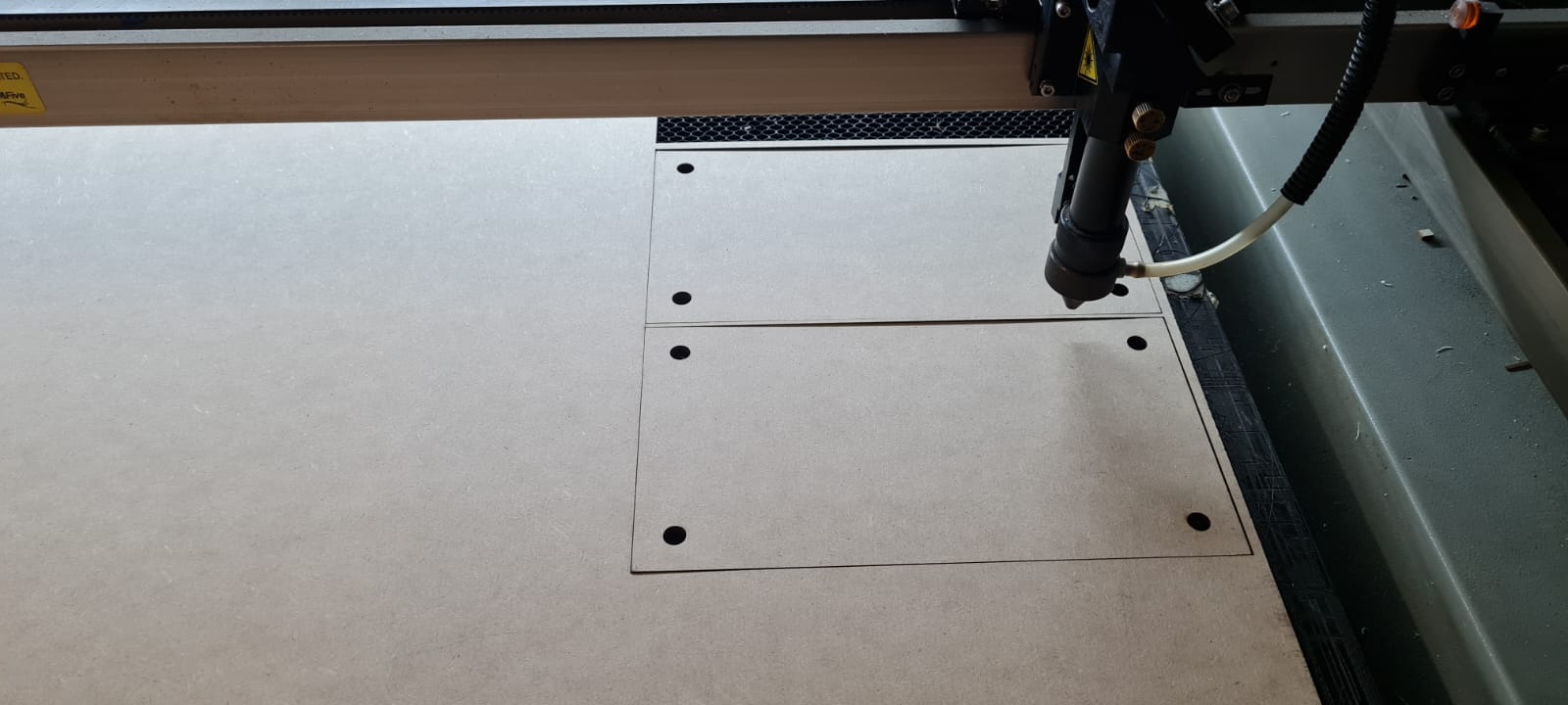
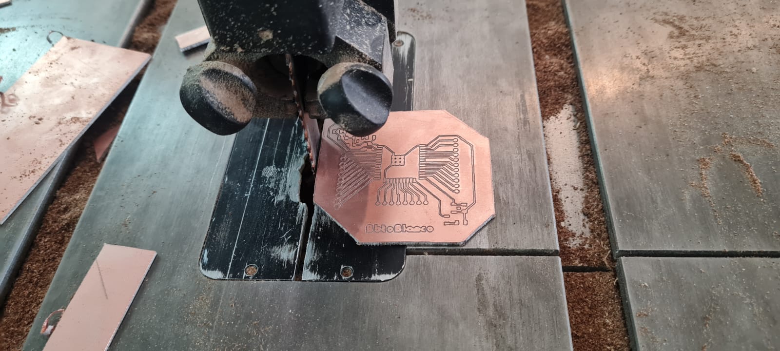
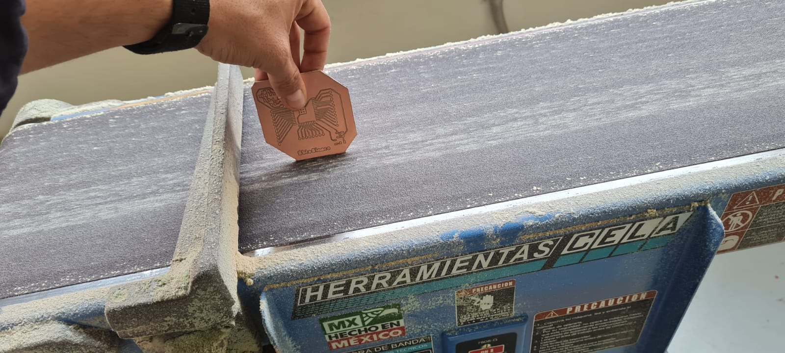
 And afterwards it was only a matter of cutting it on the shape I designed, but couldn't do it with the CNC Mill as there was a long queue to use it. I opted for the band saw and belt sander for better finishing.
Soldering
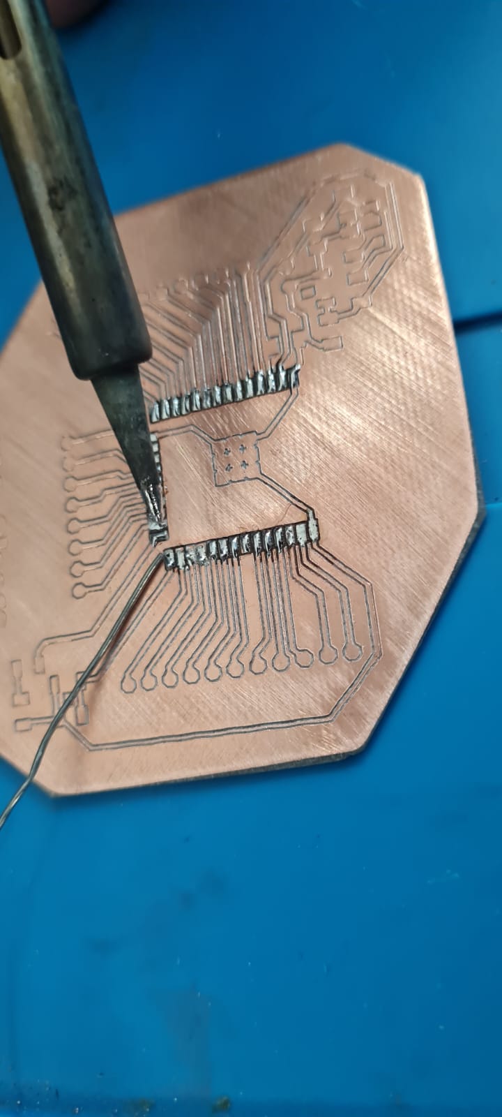
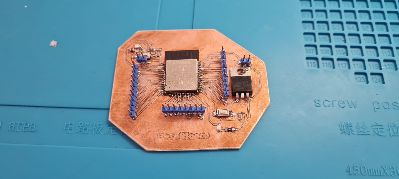
In theory, soldering is as easy as putting the component on the right place, then adding heat either using a soldering iron at 380°C or with a hot air gun (about 400°C since the air cools down faster), and then appliying soldering material for it to melt and join the component with the PCB. Of course is a bit more difficult than that as the heat applied must be very precise, the components are very small and move around a lot, and sometimes Murphy's law comes into play and any other thing may fail. After a bunch of tests, burns and time, it was possible to solder all the components in place. Unfortunately it was the first time I soldered such small components and had to unsolder a lot of times, but I must admit I'm learning a lot from this. The milling process erased a couple of routes for the pins so I had to solder thin copper wire to connect them. The rest was a very long process, but at the end it was doable. I am going to repeat the PCB for the final project with propper modifications on the PCB design and taking into account the paths that were removed. Also I do have a lot of practice to do on soldering.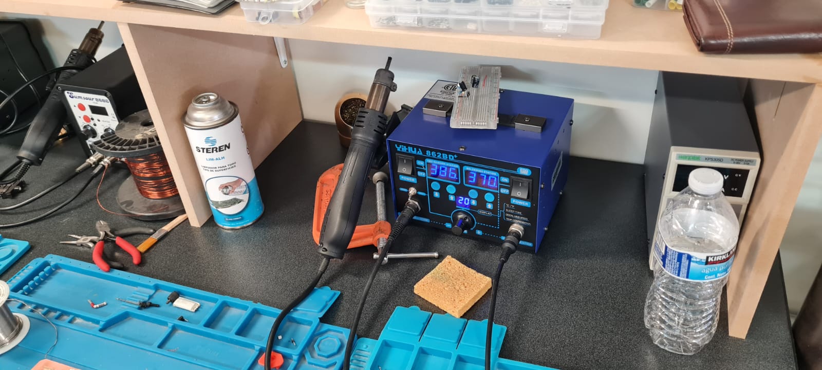
What really happened?
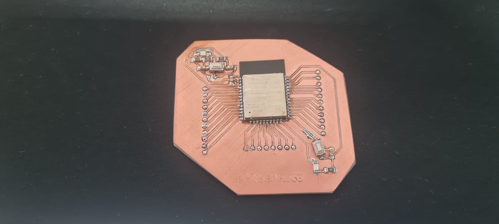
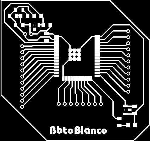
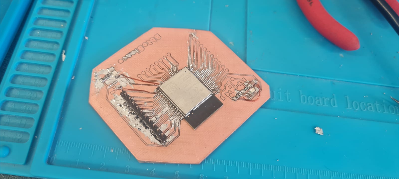
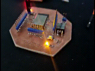
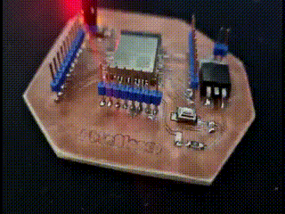
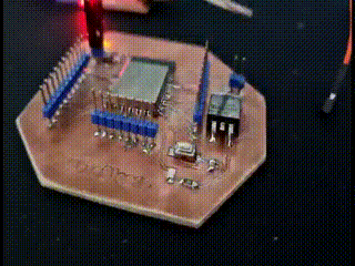
This was supposed to work on the first or second time i tried it, however the process took me about 19 different tries, changing the circuit diagram, the design of the PCB, and also several failures on the soldering of the components. However I was able to do it on the 19th iteration, for example I added a MOSFET for controlling external circuits with different voltages that the ESP32 works with, and also added a couple of LEDs for testing. Here is the final product after 19 tries.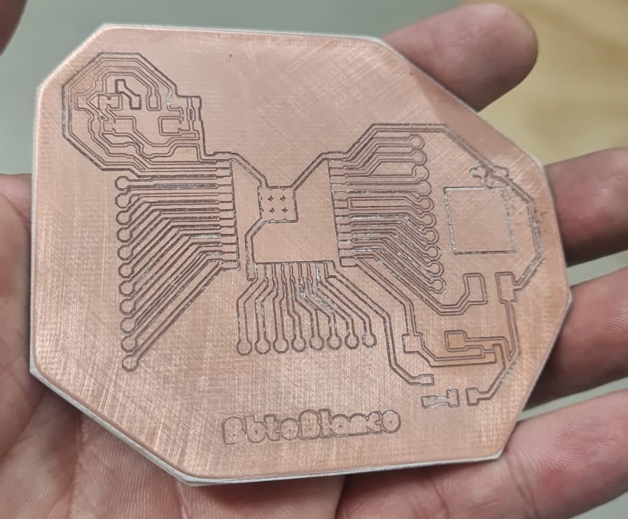
How do we know it works?
It was the time of the truth, how will it respond to programming? So i reused the random interval flickering program i designed for earlier assignments:
int X = 1000; 		//Here I'm creating the variable X, which will be the time the LED will be ON.
Int Y = 1000;		//Here I'm creating the variable Y, which will be the time the LED will be OFF.
void setup() {
pinMode(LED_BUILTIN, OUTPUT);		// initialize digital pin LED_BUILTIN as an output.
								  }
// the loop function runs over and over again forever
void loop() {
X = random(1000);                 // This line gives X a random value between 0 and 1000
Y = random(1000);                 // This line gives Y a random value between 0 and 1000
digitalWrite(LED_BUILTIN, HIGH);  // turn the LED on (HIGH is the voltage level)
delay(X);                    	  // wait for X seconds
DigitalWrite(LED_BUILTIN, LOW);   // turn the LED off by making the voltage LOW
delay(Y);                  	   // wait for Y seconds
}		//Since all this chunk of code is between the "{}" of Void Loop, it will be repeated indefinitely.
I have included the files for my pcb design, the *.png* image of the paths and holes and the gcode for milling on the Downloadables webpage. See you next week!