Week_06: Electronics Design

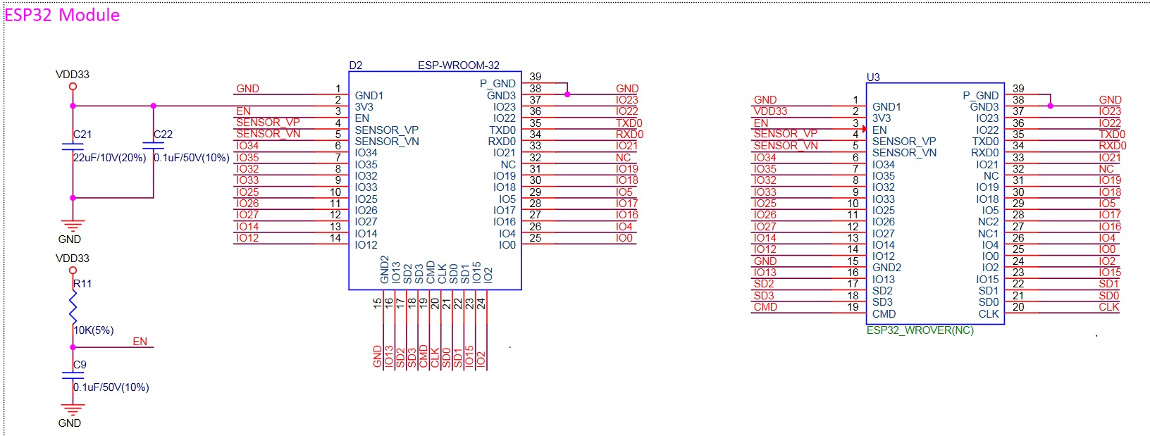
For this week's assignment the plan is to design our version of the PCB that will be used on the final project. In this PCB we embed the microcontroller that's going to be the brain
of the object, in my particular case, it is the ESP32 microcontroller, because it has WiFi and bluetooth connectivity and my project needs online information to be downloaded.
The first step is to find the electronic schematic on the manufacturers website. Afterwards, with the help
of my instructors, I determined which components, outputs and inputs I am supposed to include on the PCB for my project. My instructor recommended to include most, if not all, of the Inputs and Output pins,
because it is better to have them and not need them, than to need them and not have them.
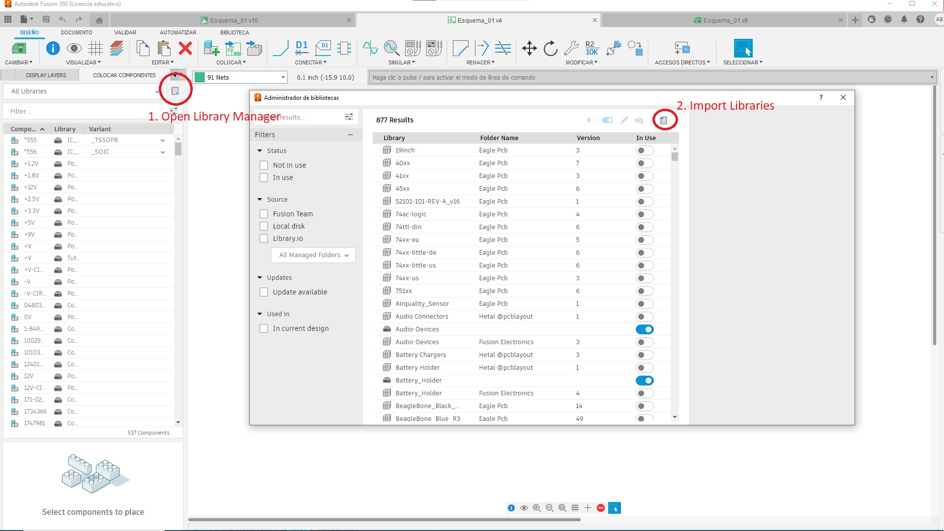
 The software to be used is Fusion 360, and first of all we need to include the library for the electronic components that will be used. So first one goes to the Component tab on the newly created Schematic file.
Then, next to the library filter drop down menu, there is the Open Library Manager button. There we have to look for the Import Libraries button, the drop down menu will include the option
Import from local disk, so there you have to download and locate the following Library, which is the FabAcademy electronics library. In this case
I downloaded the one for Fusion 360.
The software to be used is Fusion 360, and first of all we need to include the library for the electronic components that will be used. So first one goes to the Component tab on the newly created Schematic file.
Then, next to the library filter drop down menu, there is the Open Library Manager button. There we have to look for the Import Libraries button, the drop down menu will include the option
Import from local disk, so there you have to download and locate the following Library, which is the FabAcademy electronics library. In this case
I downloaded the one for Fusion 360.
 The next part is to search for the components on the library menu, and position them properly on the work space, and using the tool Network, which connects components with each other, and with
Name tool, which can invisibly connect the nodes in order to locate them in a easier manner on the definitive PCB.
The next part is to search for the components on the library menu, and position them properly on the work space, and using the tool Network, which connects components with each other, and with
Name tool, which can invisibly connect the nodes in order to locate them in a easier manner on the definitive PCB.
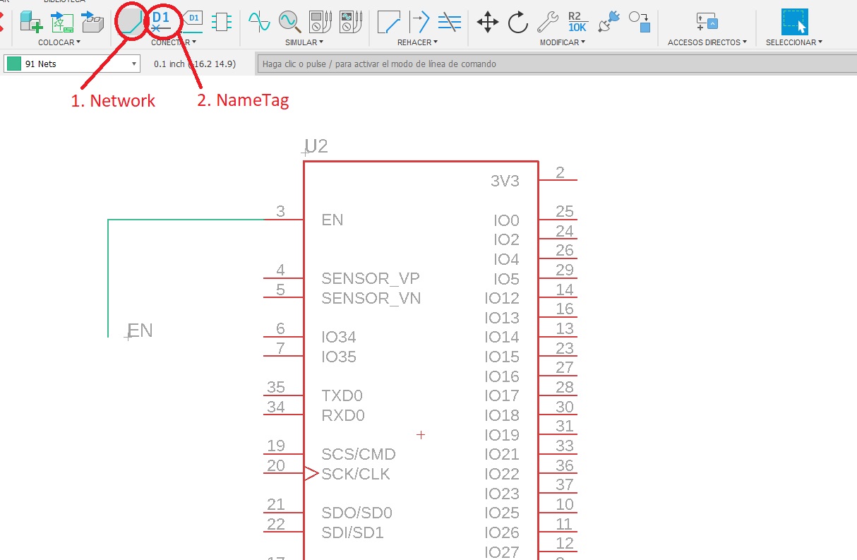 The Network Tool creates the paths connecting the different components. The tool Name, names each connection so the software knows what node is connected to which component.
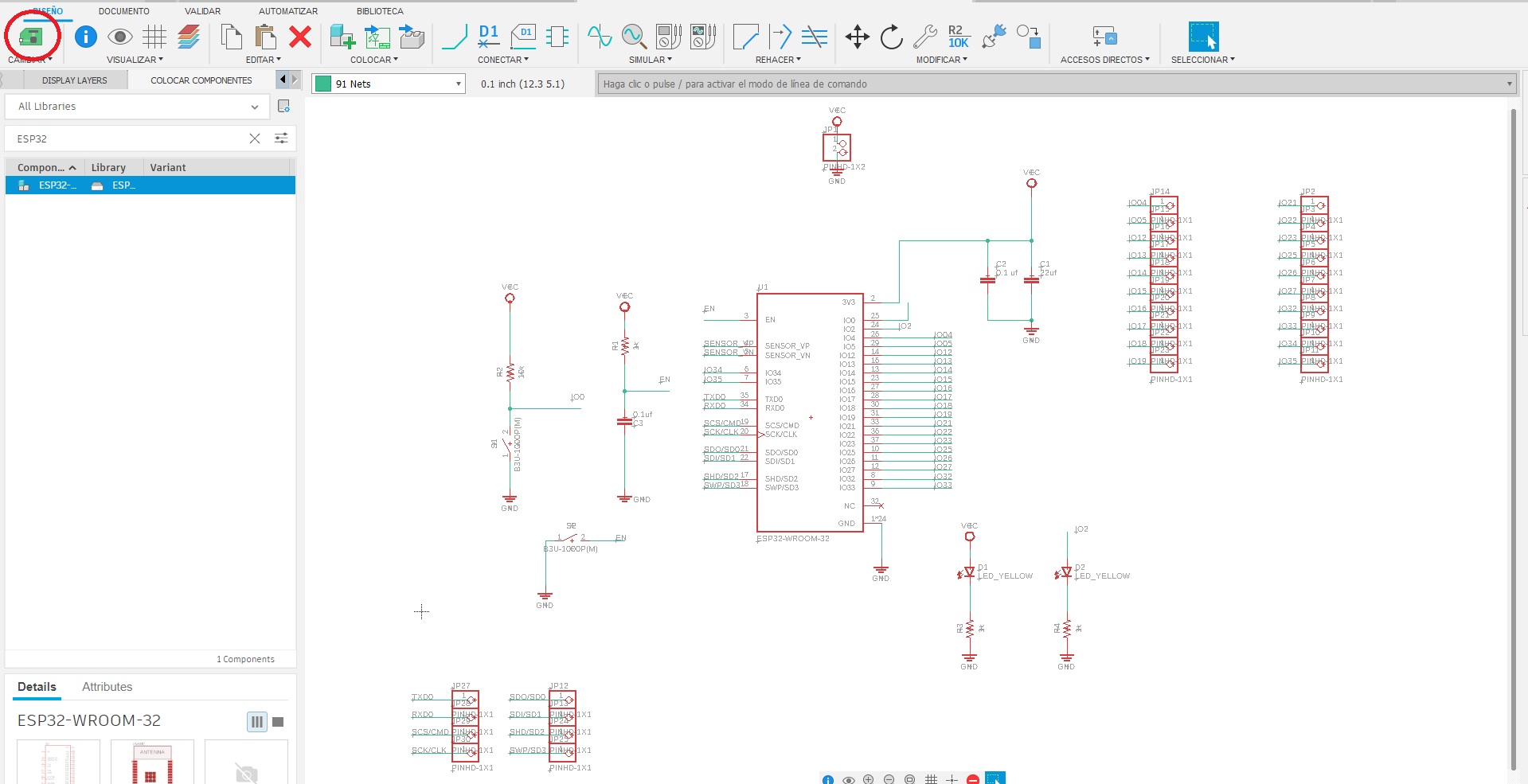
After we "copied" the schematic with the propper components and values for the resistors and capacitors, it is time to send it to the arrangement of the components, usin the Change Schematic to PCB button.
The Network Tool creates the paths connecting the different components. The tool Name, names each connection so the software knows what node is connected to which component.
After we "copied" the schematic with the propper components and values for the resistors and capacitors, it is time to send it to the arrangement of the components, usin the Change Schematic to PCB button.
 Which will show us the next screen, a really chaotic arrangement of the components we have just connected:
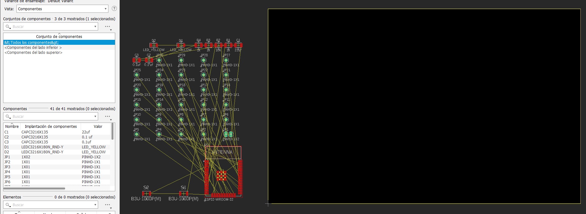 Each of the components "know" where they are supposed to be connected, that is every yellow line showed there. And the yellow/black rectangle on the left is the shape of the PCB that we are using. But don't worry as we can design the
shape of the final PCB with vectors through Fusion 360 as I will explain later on.
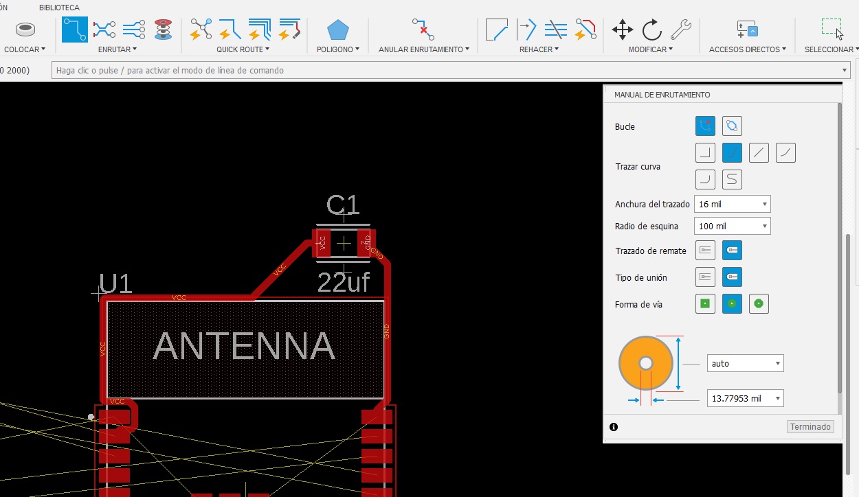
Once we have arranged everything on a confortable and functional manner, we use either the Manual Routing or Quick Routing tools for connecting the components with propper copper PCB lining. In this menu, one can select
the wiring width, the shape for the through-hole component connection, and the kind of angles the route must follow.
Each of the components "know" where they are supposed to be connected, that is every yellow line showed there. And the yellow/black rectangle on the left is the shape of the PCB that we are using. But don't worry as we can design the
shape of the final PCB with vectors through Fusion 360 as I will explain later on.
Once we have arranged everything on a confortable and functional manner, we use either the Manual Routing or Quick Routing tools for connecting the components with propper copper PCB lining. In this menu, one can select
the wiring width, the shape for the through-hole component connection, and the kind of angles the route must follow.
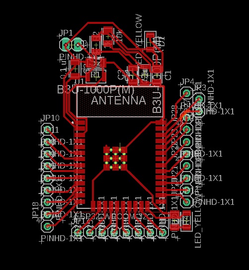
 And after a lot of work, trial and error, the final PCB started looking like a professional Printed Circuit Board, still a bit chaotic but functional.
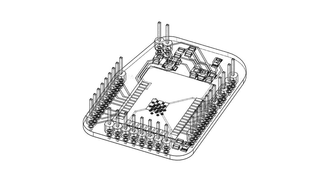
 The next part is to pass it to the 3D PCB workspace, through the button Transfer to 3D PCB on the upper left part. And it looks something like this:
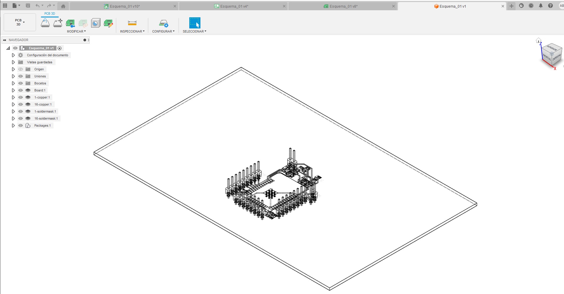 It's worth saying that the buttons for going to the different workspaces Transfer to 3D PCB and Change schematic to PCB, are used also to update changes on each of the previous workspace. For example
if one changes the resistors dimension using different components on the schematics workspace, it is necessary to update on the following step through this buttons.
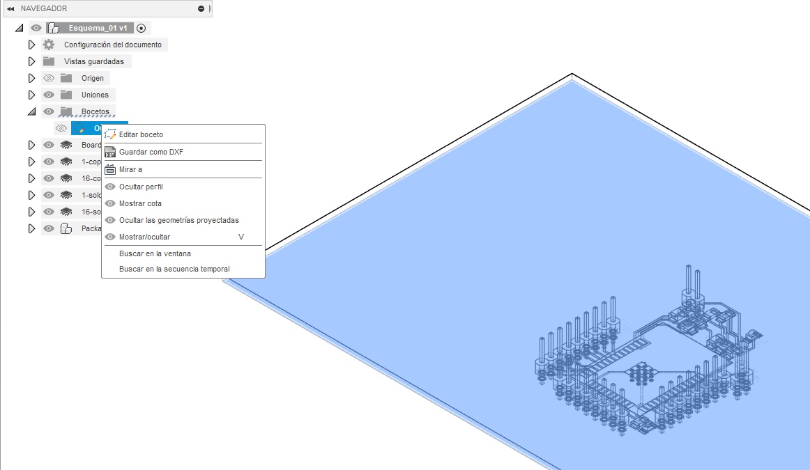
That said, the PCB needed to look cool besides working correctly, so I gave myself the task to design the shape for the PCB, as the arrangement was completed. This is done through the
Edit Sketch option on the drop down menu for the sketches tab.
It's worth saying that the buttons for going to the different workspaces Transfer to 3D PCB and Change schematic to PCB, are used also to update changes on each of the previous workspace. For example
if one changes the resistors dimension using different components on the schematics workspace, it is necessary to update on the following step through this buttons.
That said, the PCB needed to look cool besides working correctly, so I gave myself the task to design the shape for the PCB, as the arrangement was completed. This is done through the
Edit Sketch option on the drop down menu for the sketches tab.
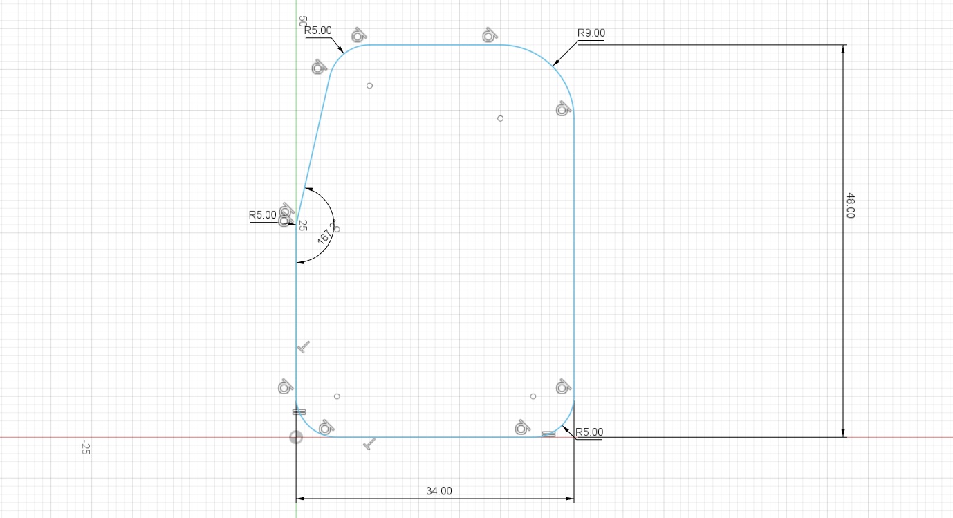
 On that sketch I drew and measured the shapes until I ended up with a cool-looking PCB for my final project.
The tests
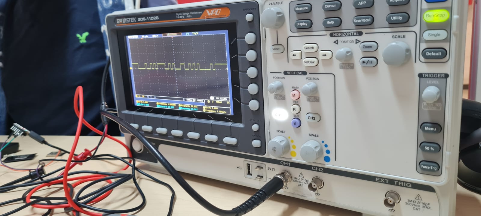
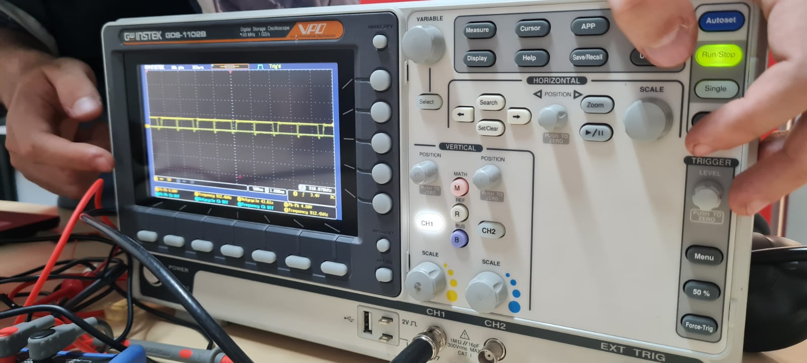
The group-oriented part of the assignement is to use different measuring devices on the circuit boards we have worked with previously. In this case we worked with the ESP32 and the Xiao-RP2040, and the measuring devices were an oscilloscope and a multimeter, both used for electronic signals recognition and graphing. The circuit we used on both tests is a Xiao-RP2040 programmed with a simple blinking LED code.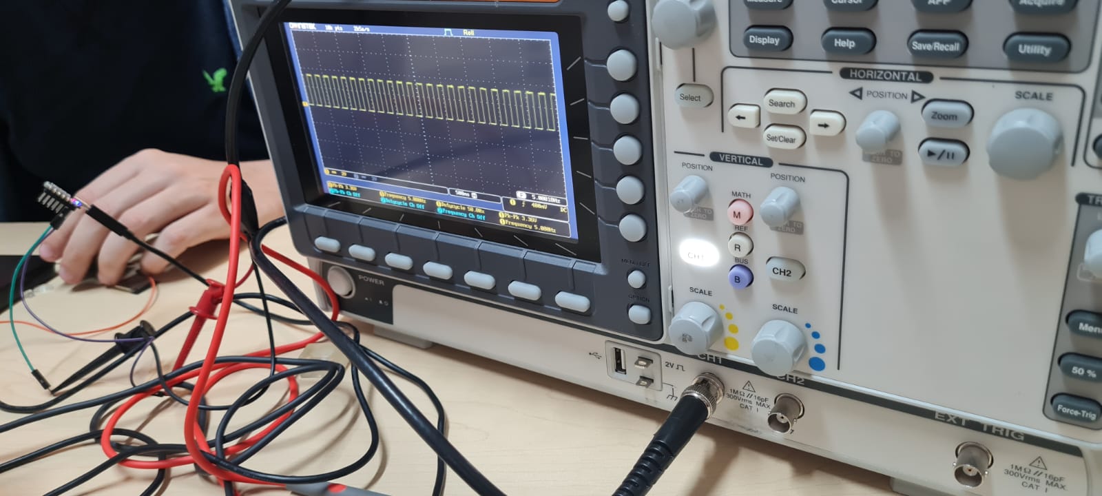
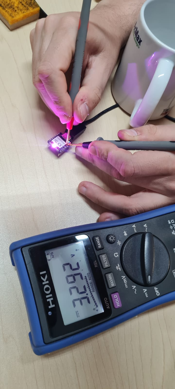
A and H as output, which was read by the osciloscope and interpreted through the waves.
I have included the schematics file for my PCB, along with the links for downloading the different libraries for Fusion 360 on the Downloadables webpage. See you next week!