This assignment focuses on creating and testing a microcontroller
development board. The goal is to design a versatile platform for
microcontroller applications. Key tasks involve carefully planning the
board layout and including essential components like LEDs, resistors,
and specific connectors
Research:
EasyEDA
EasyEDA is a free, web-based Electronic Design Automation (EDA) software
that allows users to create schematic diagrams, printed circuit board
(PCB) layouts, and simulations for electronic projects. It provides a
user-friendly interface and a wide range of components and modules that
users can use to design and test their electronic circuits.
With EasyEDA, users can design their circuits by dragging and dropping
components onto a canvas, and then connecting them together with wires.
They can also simulate the circuits to test their functionality and
performance, and generate a PCB layout for their circuit design.
EasyEDA also provides a large library of components that users can use
in their circuit designs, including microcontrollers, sensors, power
supplies, and more. It also has a collaboration feature that allows
multiple users to work on the same project simultaneously.
Design process:
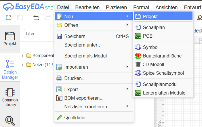
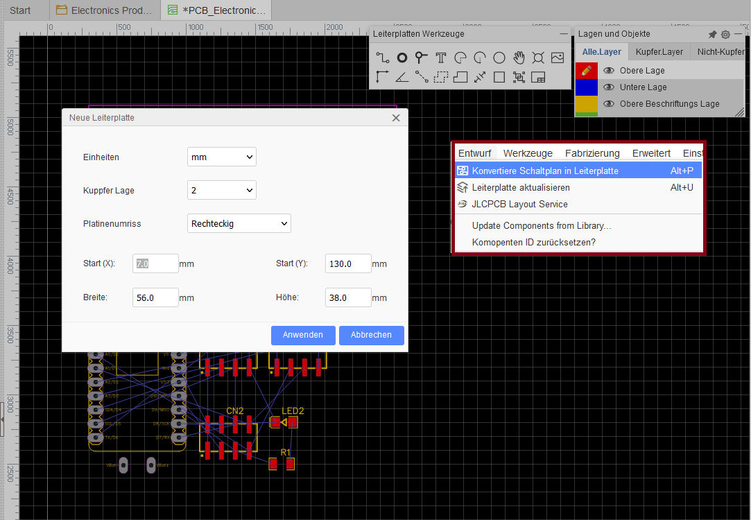
1. Initiate a new project:
The inaugural stage involves the initiation of a new project within the
EasyEDA environment. To commence this process, navigate to the "File"
menu, followed by the selection of "New" and afterward "Project."
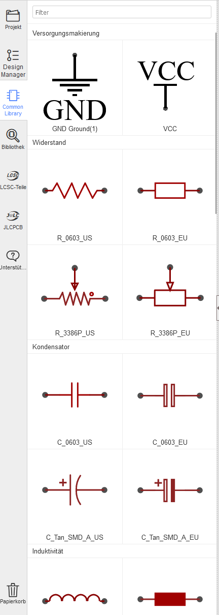
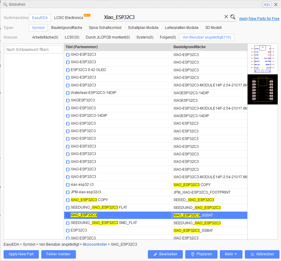
2. Searching the components footprints:
In the second phase of the process, I initiated a search within the
Common Library for commonly used components, such as LED,
FEMALE-HEADER-2.54-SMD-8, and resistors. Subsequently, I used the
cloud-connected library to identify additional components like the
ESP32.
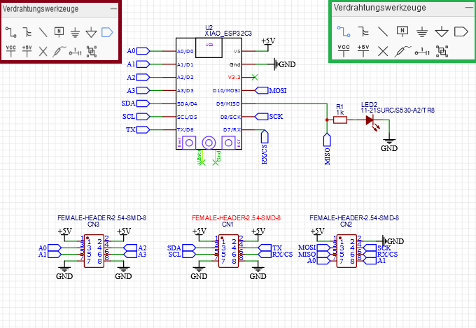
3. Placing the components and creating connections
Following the placement of components, I used the netflag feature, as
indicated by red markings in the accompanying pictures, to establish
connections between the components and enhance the overall clarity and
organization of the circuit. Subsequently, I utilized the wire function,
as illustrated by green markings in the pictures, to further refine and
establish the necessary electrical connections within the circuit
design.
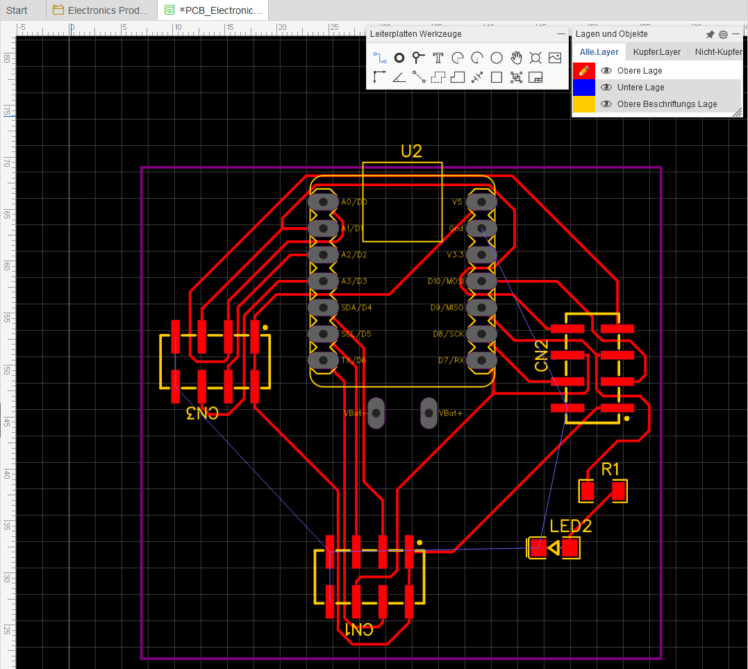
4. Convert Schematic to PCB and place the electronic components
In this phase, the circuit is transformed into a PCB file by navigating
to "Design" and selecting "Convert Schematic to PCB." Following this
conversion, the dimensions of the board outline are to be selected. It's
worth noting that these dimensions can be adjusted later or even
imported as a DXF file. At this point, components are placed on the
board as per the desired configuration
5. Establishing Electrical Connections
Continuing with the process, I employed the wiring tool to establish
connections between the pads on the PCB, aligning them with the
specifications outlined in the schematic. This step involves
systematically linking the various components on the board, ensuring
that the electrical pathways accurately reflect the intended circuit
design
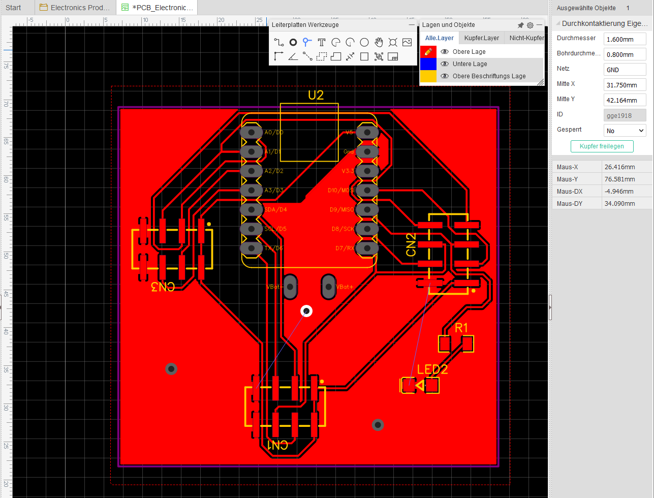
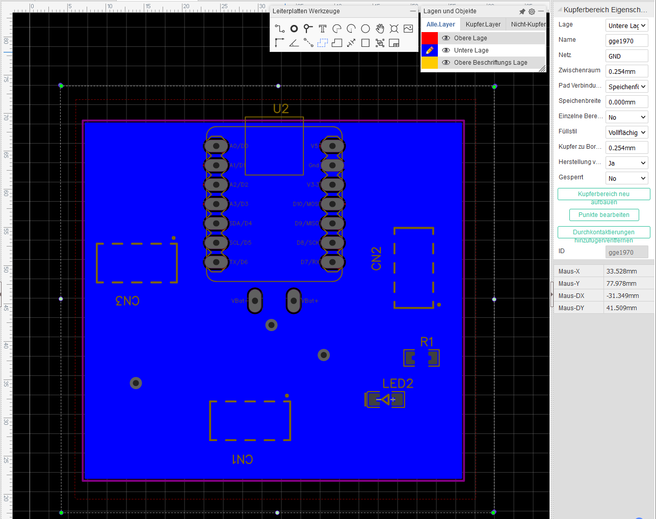
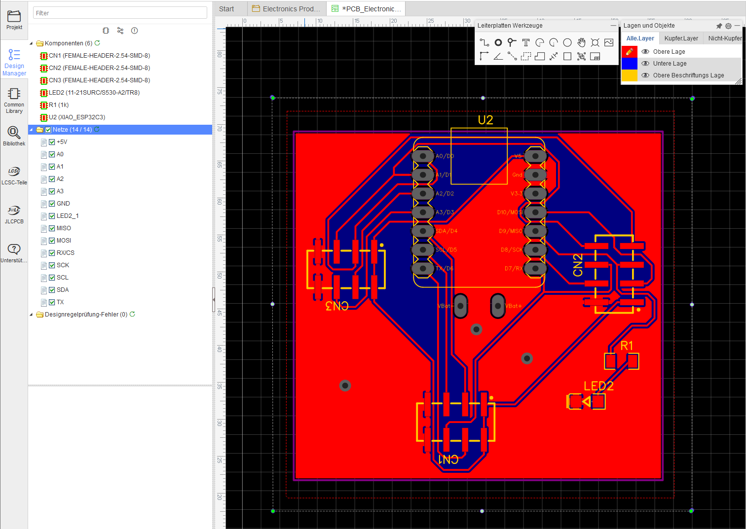
6. Ground Plane and Via Implementation
I employed the Copper Area function to designate specific regions on the
PCB where the copper is connected to the GND (Ground) signal. To
establish a connection between the GND signal on different sides of the
PCB, I utilized vias. These vias serve as conduits, allowing the GND
signal to traverse seamlessly from one layer to another, ensuring a
well-connected and optimized grounding system throughout the
microcontroller development board.
In a parallel process on the second layer of the PCB, I again utilized
the Copper Area function to delineate areas where copper is linked to
the GND (Ground) signal.
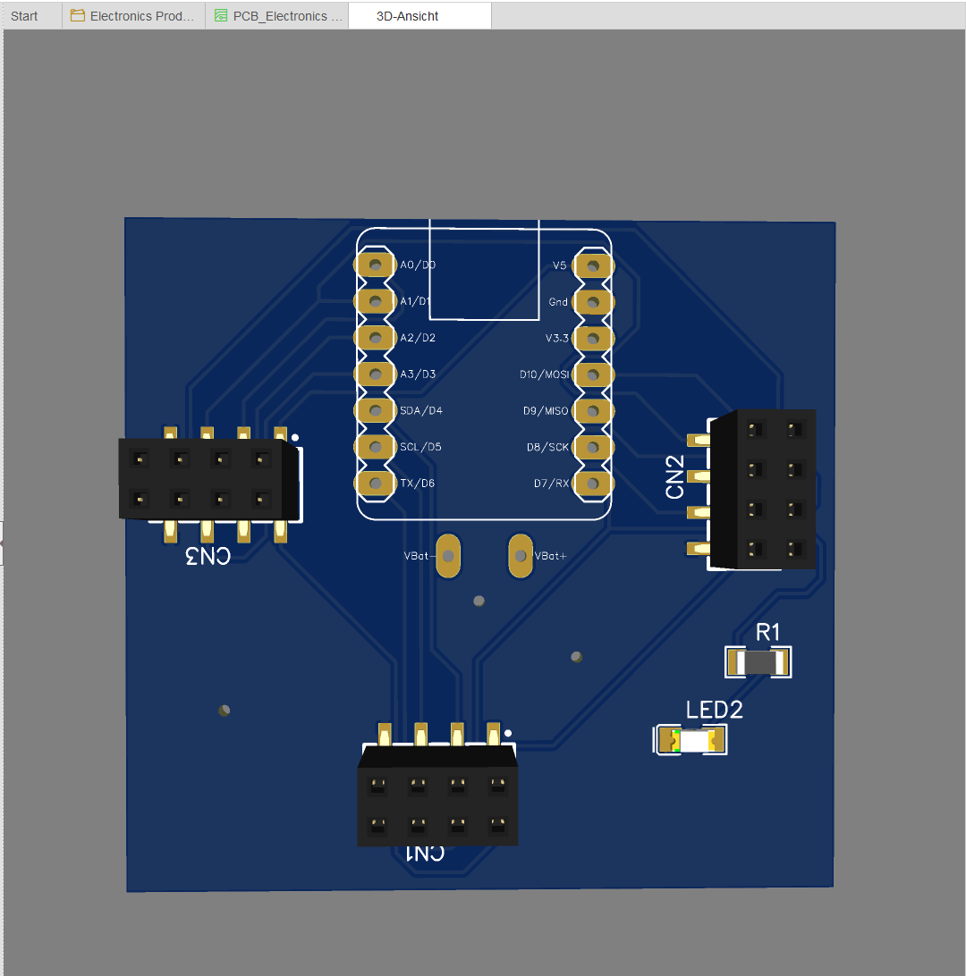
7. Design rule check and 3D-Vizualization
In this step, it is imperative to perform a Design Rule Check (DRC)
before proceeding to visualize the PCB in 3D and generating the
essential Gerber files required for fabrication. The DRC ensures
adherence to design guidelines and identifies potential issues that may
impact the functionality and manufacturability of the microcontroller
development board. Once the DRC validation is successfully completed,
the PCB can be visualized in three dimensions, providing a comprehensive
overview of the design. Following this visual inspection, the final step
involves generating the Gerber files, crucial documents necessary for
the fabrication process.
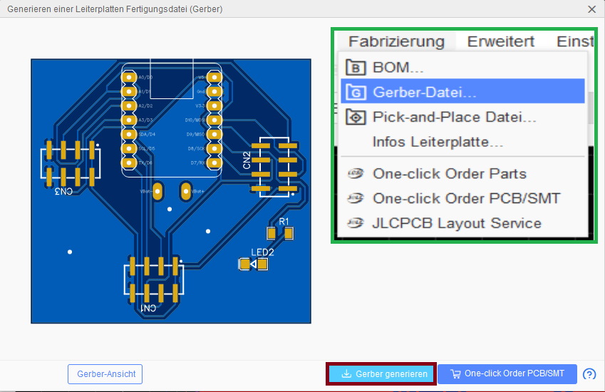
8. Generating Fabrication Files for PCB Production
In the upcoming phase, the creation of Gerber files is initiated by
navigating to "Fabrication" and selecting "PCB Fabrication File," as
indicated by the green markings in the accompanying images.
Subsequently, the process involves clicking the "Generate Gerber"
button, highlighted in red within the pictures below.
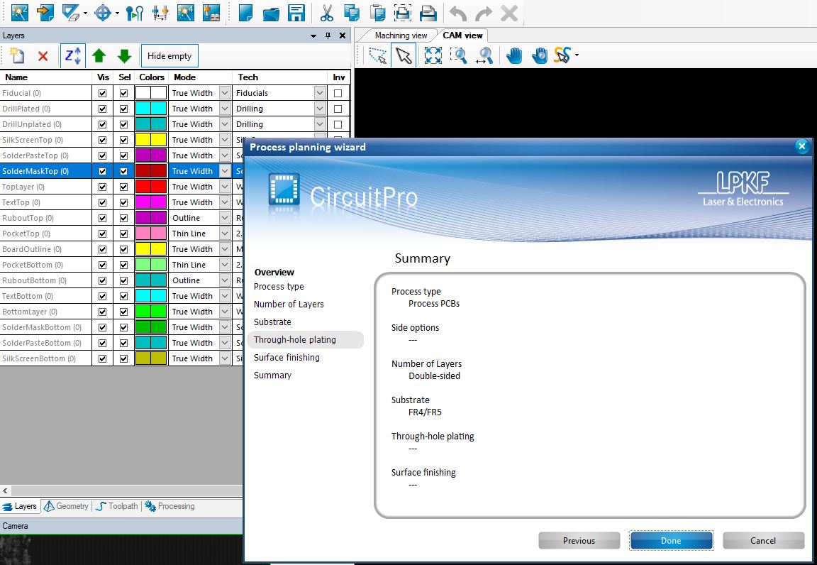
Processing the PCB with LPKF
1. Start Process Planning Wizard: I begin by launching the process planning wizard on the LPKF machine
interface. This guides me through the initial setup steps.
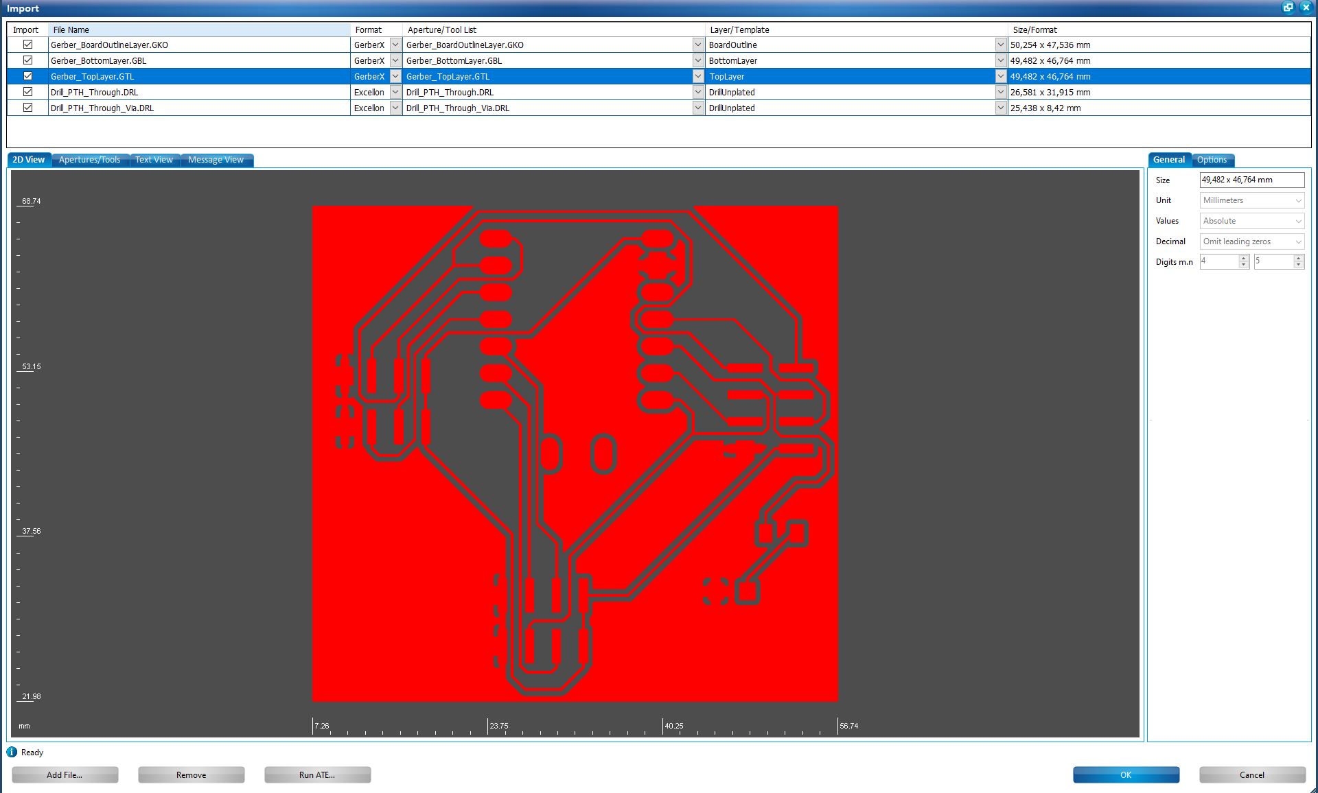
2. Import Data from a Non-Native Format: I import my PCB design data from a non-native format. I
ensure the data is correctly formatted and compatible with the LPKF software.
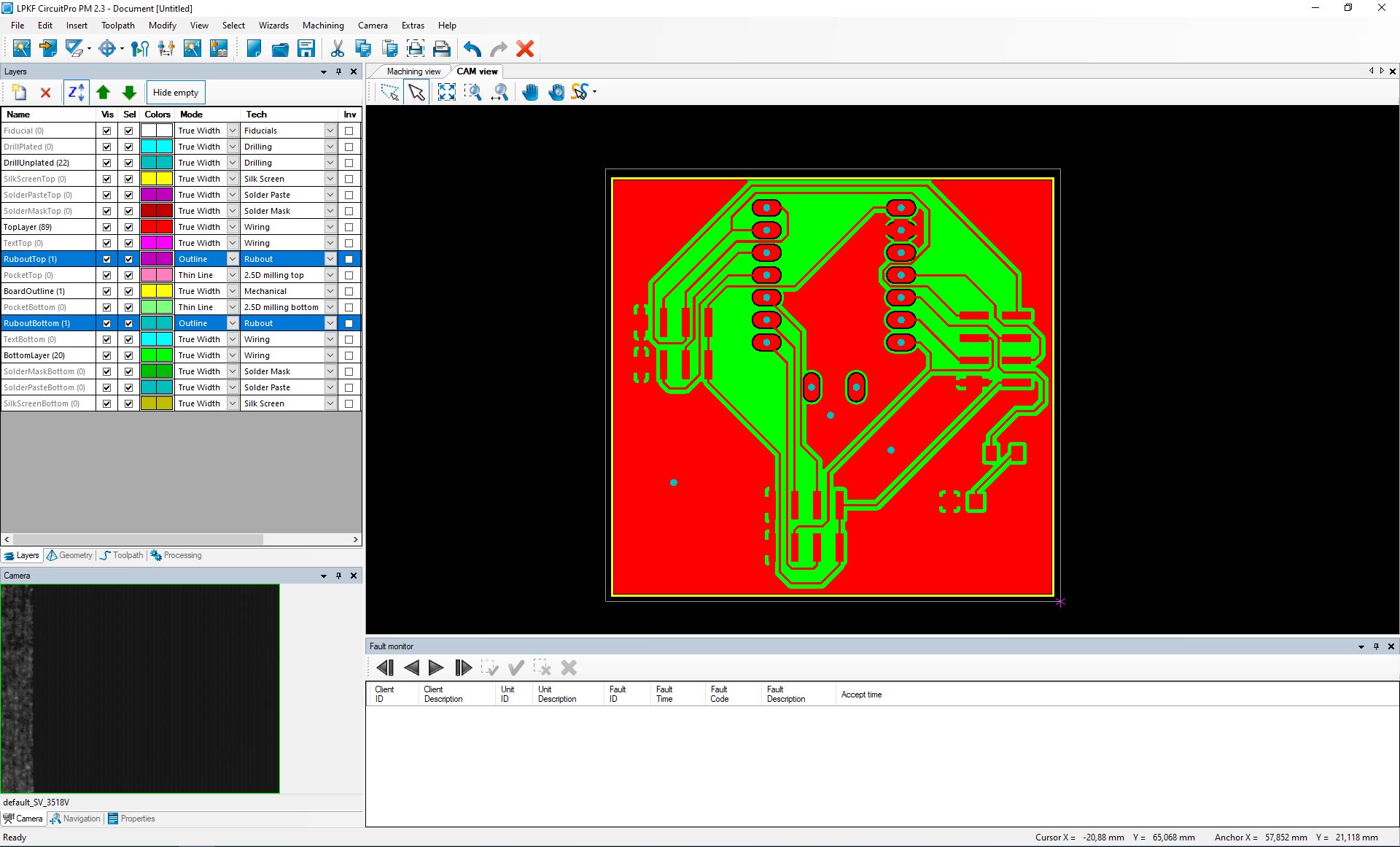
3. Create an Area for Unnecessary Copper Removal (Rubout): I define the areas on my PCB where
unnecessary copper needs to be removed. This process, known as rubout, helps to clear out excess material.
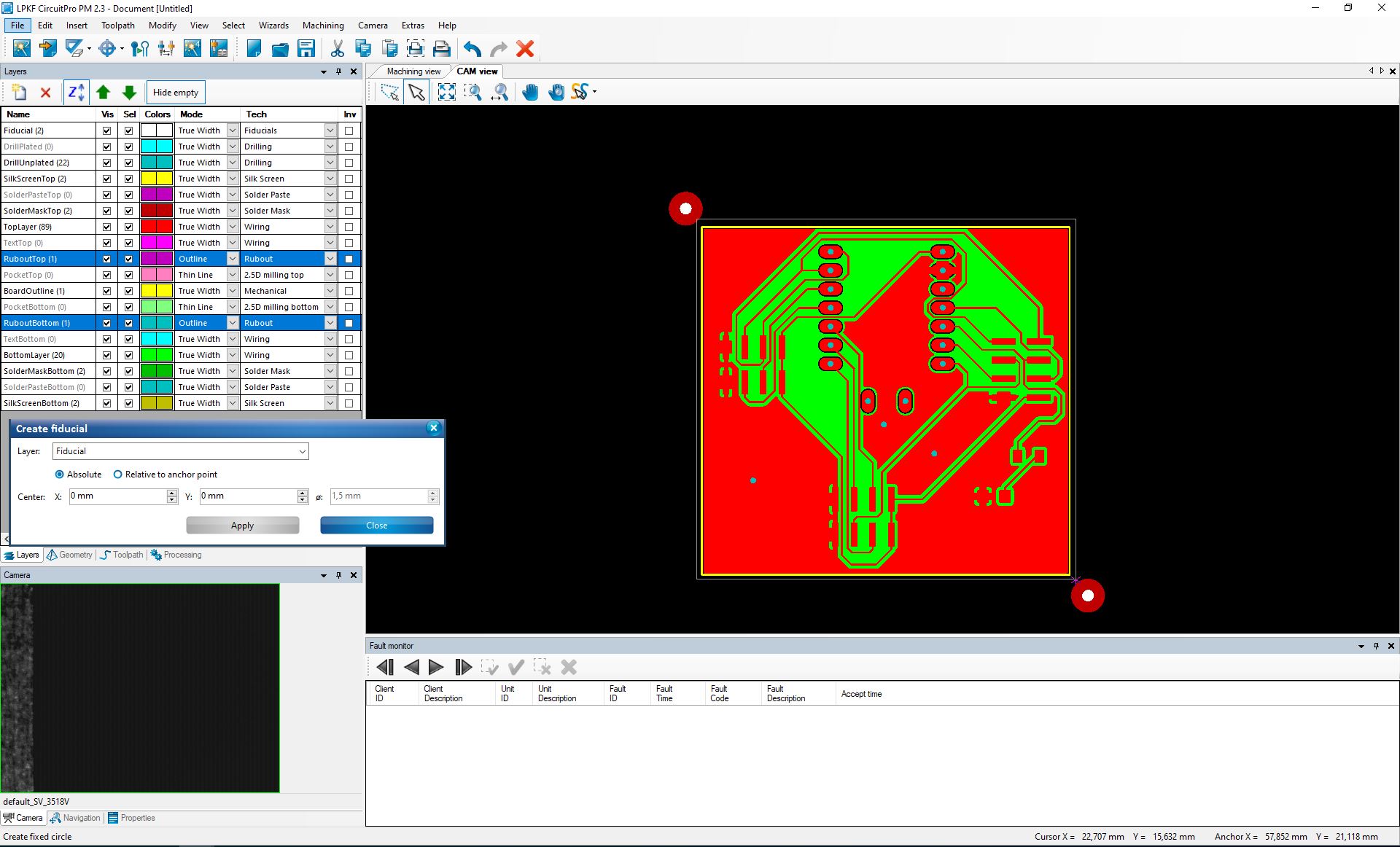
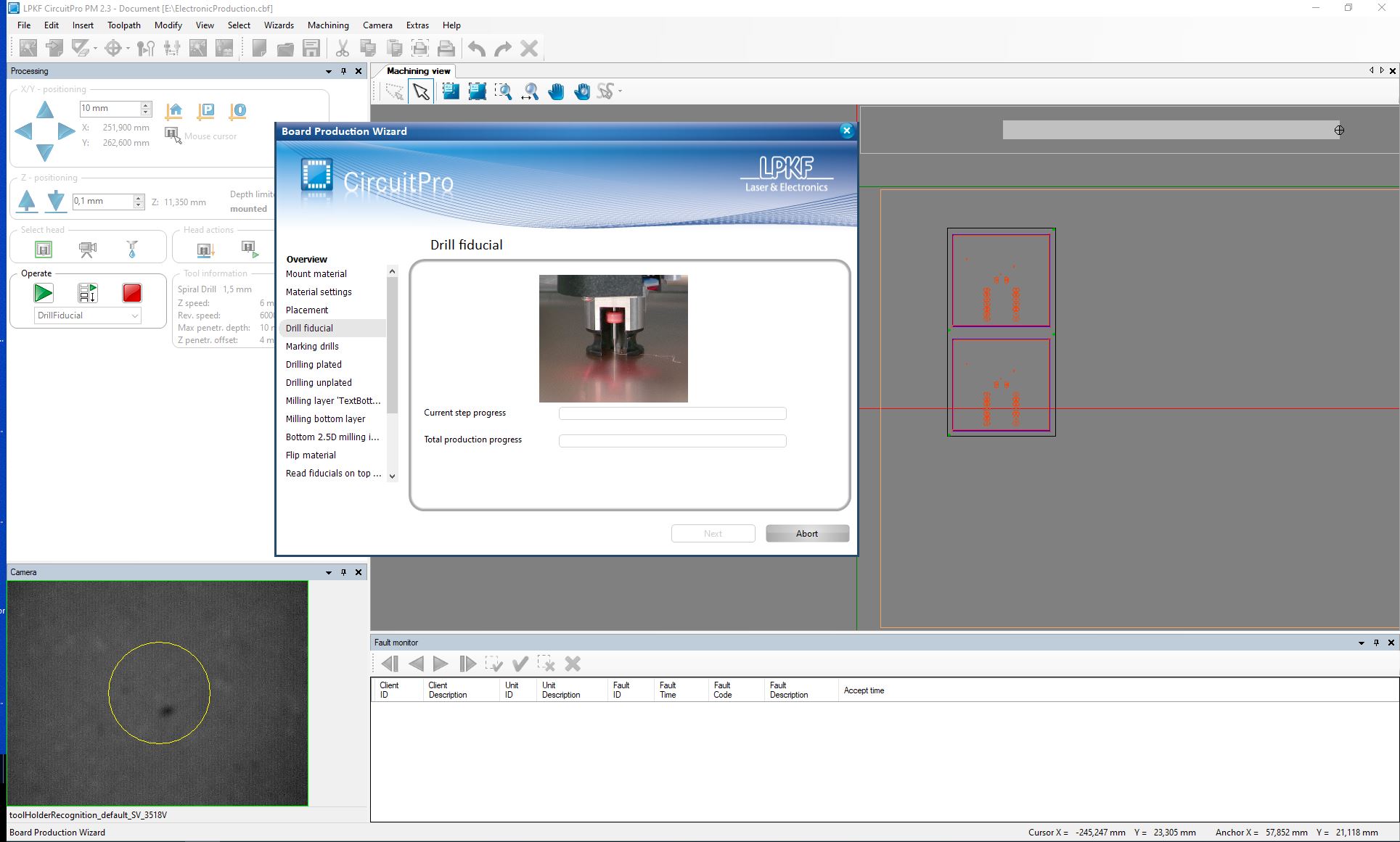
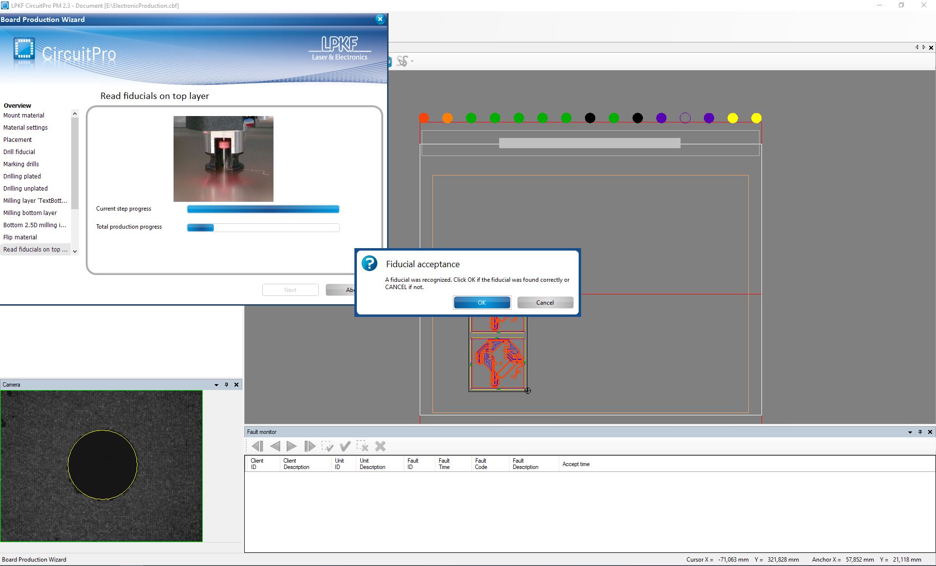
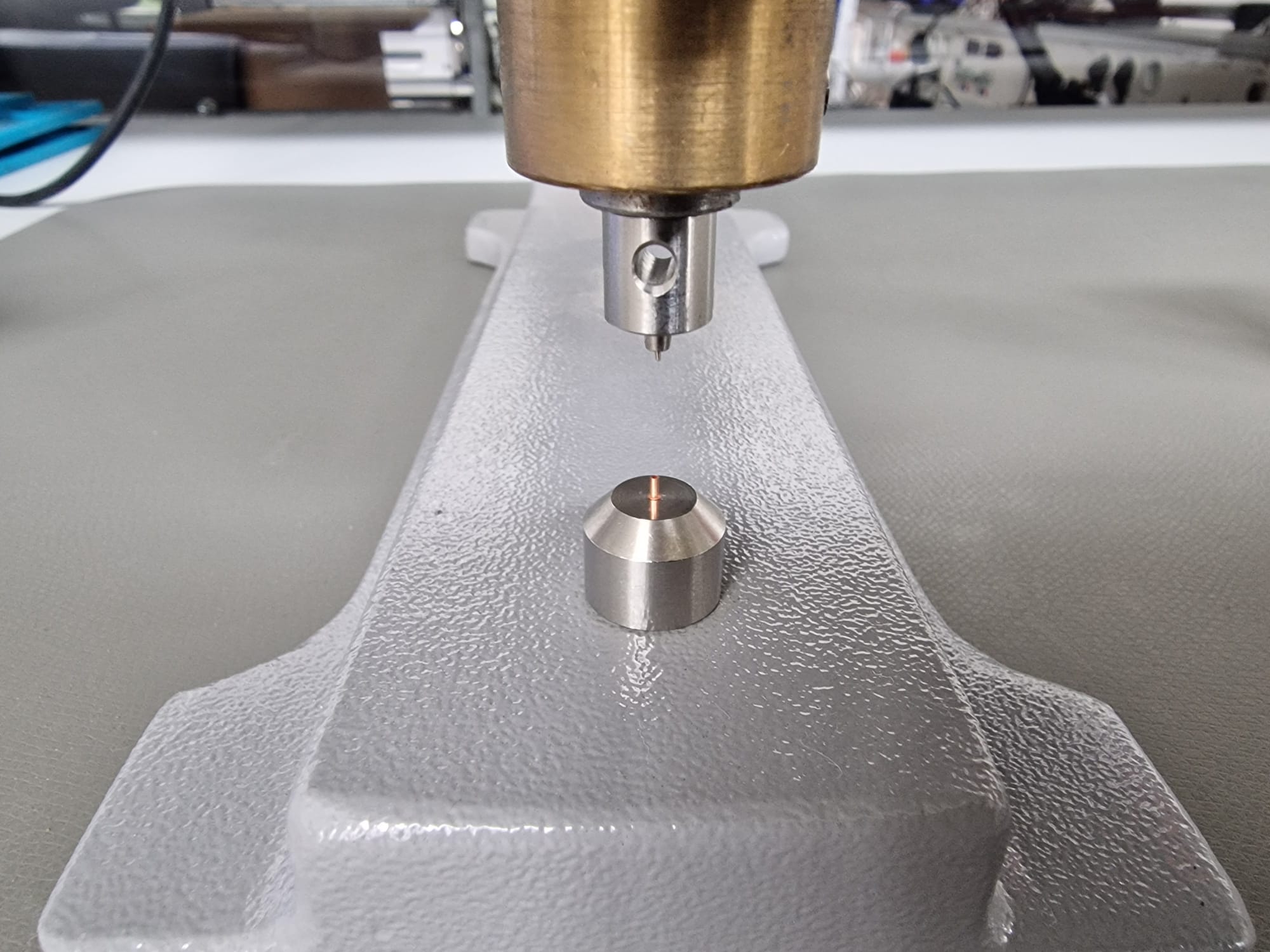
4. Create Fiducials in the CAM View: In the CAM (Computer-Aided Manufacturing) view, I create
fiducials. These are reference points used to ensure accurate alignment and placement during the manufacturing
process.
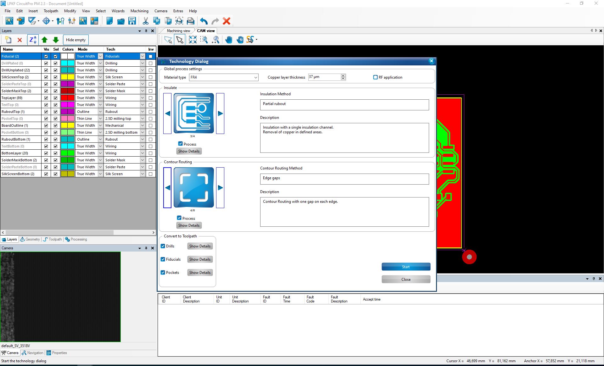
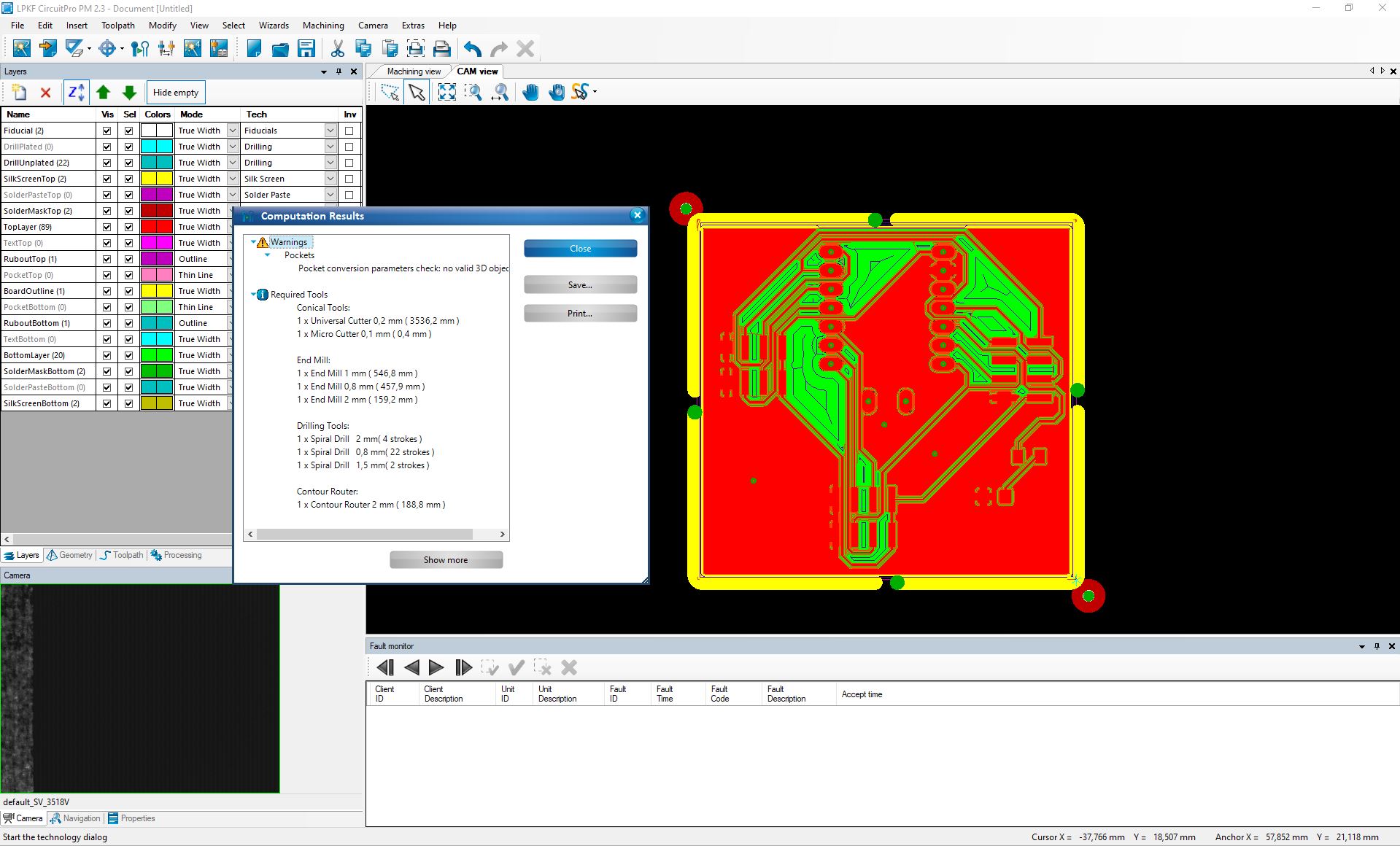
5. Generate Insulation and Contour Routing Toolpath: I generate the toolpath for insulation and
contour routing. This step involves creating paths for the machine to follow, ensuring precise cutting and
insulation of the PCB tracks. Setting: copper layer thickness: 50 µm, Insulation method: partial/full rubout,
contour routing .
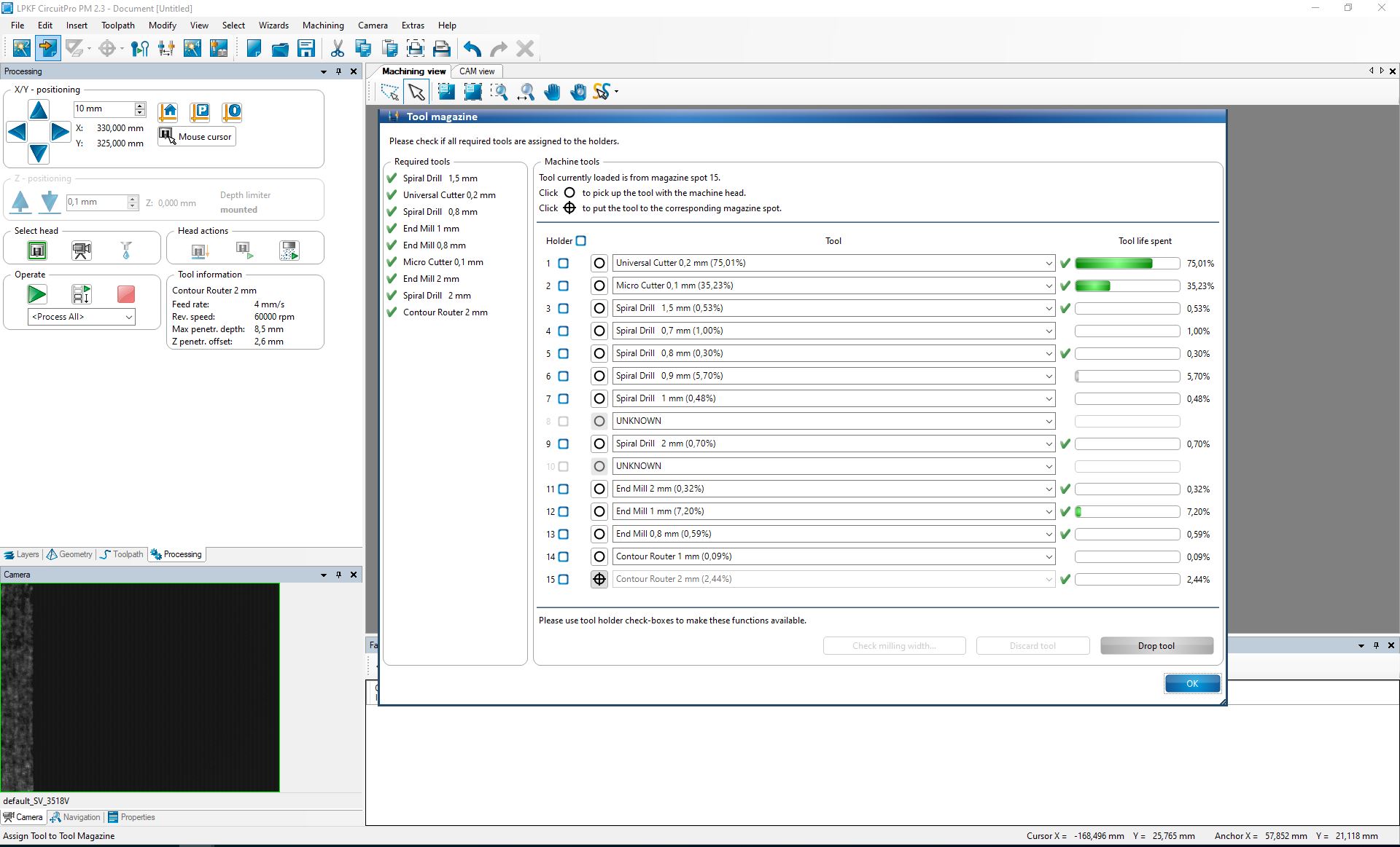
6. Open Dialog to Edit the Content of the Tool Magazine: I access the dialog box to edit the tool
magazine's content. This allows me to manage and adjust the tools that will be used during the PCB manufacturing
process.
Tools Used
Conical Tools
Universal Cutter 0.2 mm
Universal Cutter 0.1 mm
End Mill
End Mill 1 mm
End Mill 2 mm
Drilling Tools
Spiral Drill 0.6 mm
Spiral Drill 0.8 mm
Spiral Drill 1 mm
Spiral Drill 1.5 mm
Contour Router
Contour Router 2 mm
7. Start the Production Wizard and Material Setting: I initiate the production wizard and configure
the material settings. This involves specifying the type of material I am using and any relevant production
parameters.
8. Flip the Board for Second Layer Job: Once the first layer is completed, I flip the board to start
the job for the second layer. I ensure the board is properly aligned and secured before continuing.
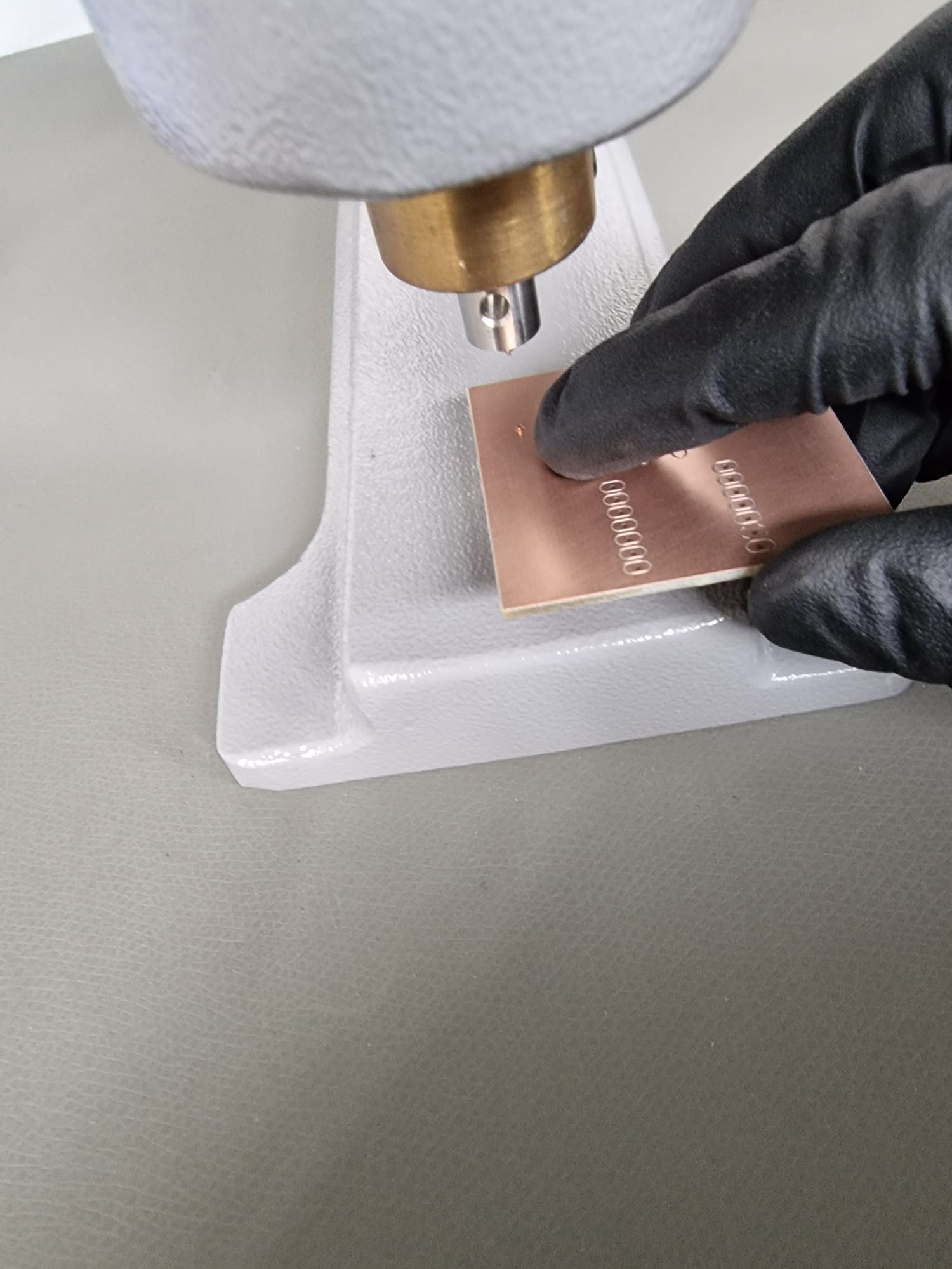
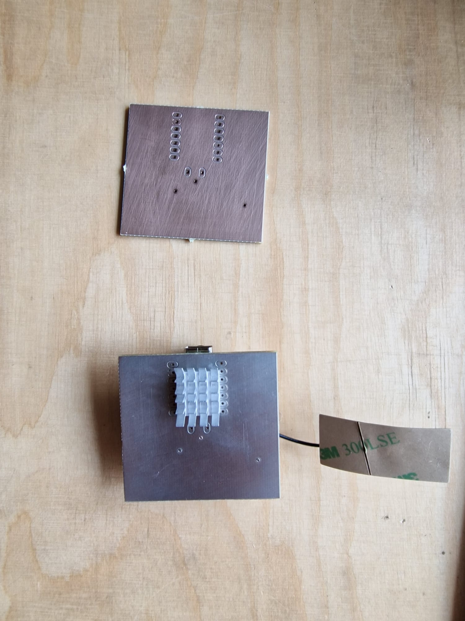
Results:
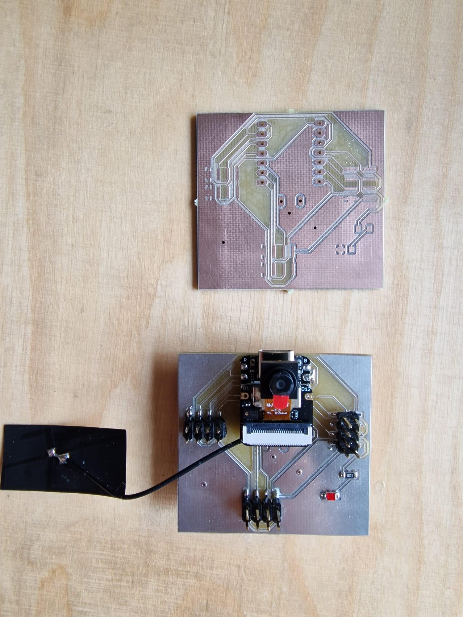
The video captures the LPKF machine milling the FR4 PCB. Before milling, I placed the via-rivets
and applied a tin-coating. After milling, I performed a manual soldering process, which involves several steps:
preparing and cleaning the components and PCB, positioning the components accurately, applying flux, heating the
soldering iron to the appropriate temperature, and soldering each connection carefully. Post-soldering, I inspect
the joints for quality, clean any flux residues, and conduct electrical tests to ensure proper functionality.
I tested the functionality of an ESP32-S3 chip that I have soldered onto a printed circuit board (PCB). My
objective is to interface the chip with a potentiometer, which acts as a variable resistor. As I adjust the
potentiometer, I change the voltage input to one of the chip's analog pins. This method allows me to perform an
analog-to-digital conversion, which helps me monitor the position of the potentiometer. The data I collect from this
test will be used to either control other components or simply to display the readings. This experiment is crucial
as it not only confirms the operational status of my chip but also serves as a foundation for future projects that
will process sensor data.
// Define the analog pin where my potentiometer is connected
const int potPin = A0;

void setup() {
  // Begin serial communication at a baud rate of 9600
  Serial.begin(9600);
  // Set the ADC resolution to 12 bits
  analogReadResolution(12);
}

void loop() {
  // Read the value from my potentiometer
  int potValue = analogRead(potPin);
  // Calculate the voltage from the ADC value (assuming a 3.3V reference voltage)
  float voltage = potValue * (3.3 / 4095.0);
  // Output the voltage reading to the Serial Monitor
  Serial.print("My Potentiometer Voltage: ");
  Serial.print(voltage);
  Serial.println("V");
  // Wait a bit before the next read
  delay(100);
}