8. Electronics Production
group assignment:
characterize the design rules for your in-house PCB production process
extra credit: send a PCB out to a board house
individual assignment:
make and test the development board that you designed to interact and communicate with an embedded microcontroller
extra credit: make it with another process
Individual assignment
In this week I constructed the pcb I desined two weeks ago:
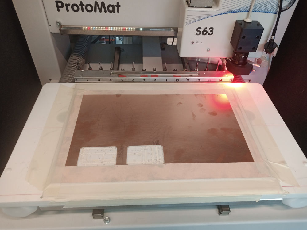
We used a LPKF Protomat 63S milling cutter to mill our pcbs.
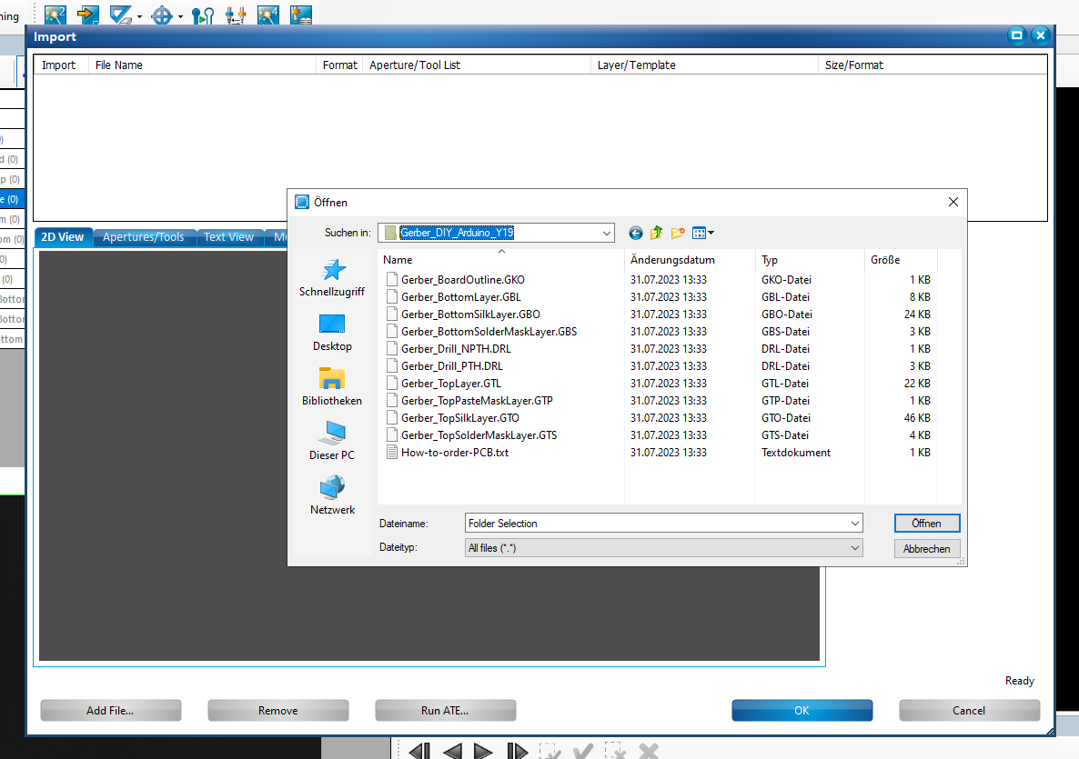
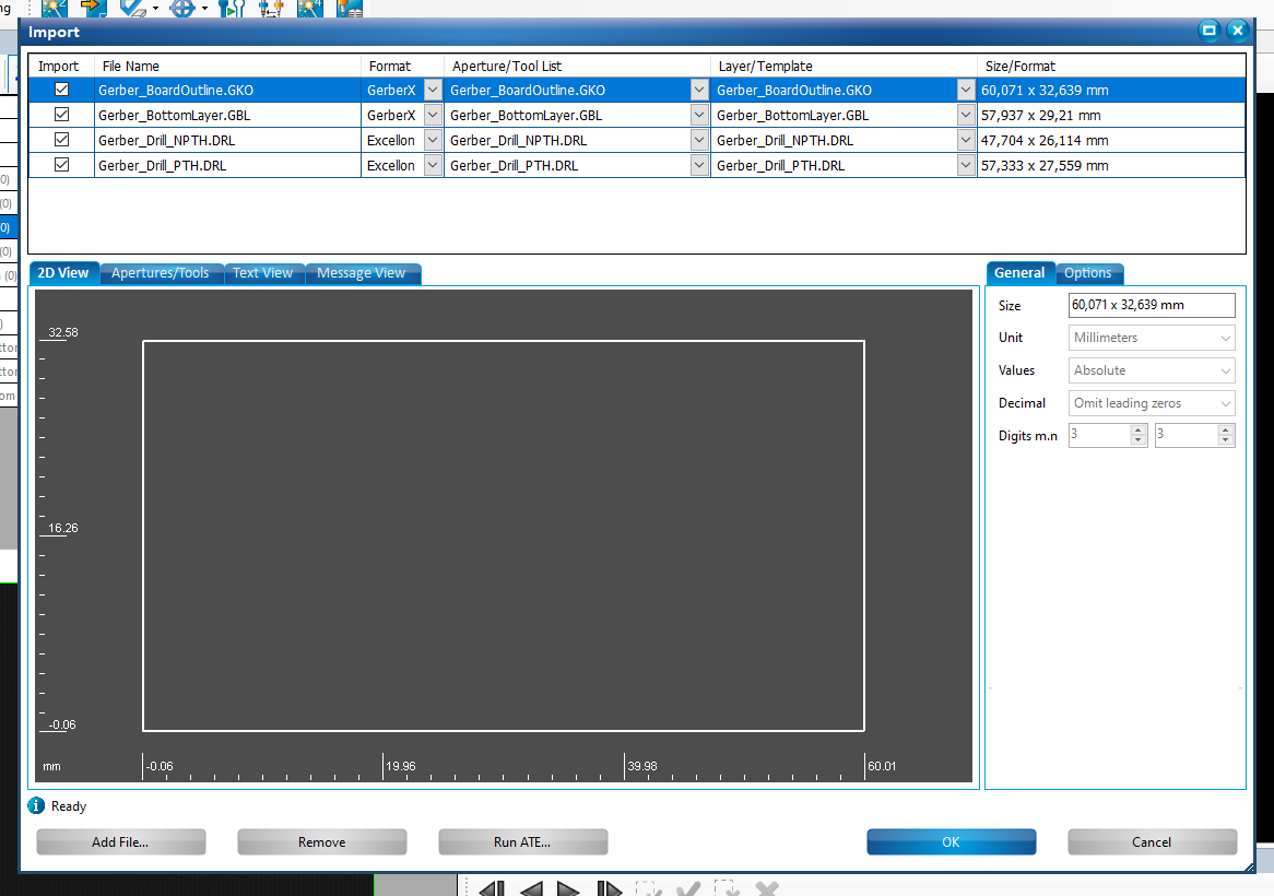
We exported gerber files from Fusion 360 (Fertigen - CAM-Vorschau - CAM… - Gerber (links anklicken) - Job verarbeiten).
For my pcb we only needed the copper top file and the outline of the pcb.
We used mills with diameters from 0.1 to 2 mm.
At the first try the copper traces were quite thin, so one of the traces was cut during the milling. So I increased the width of the traces from 6 to 10 mil and optimised the path of one trace. But this time, the traced between the legs of the ATtiny85 were cut, so I decided to use the first pcb.
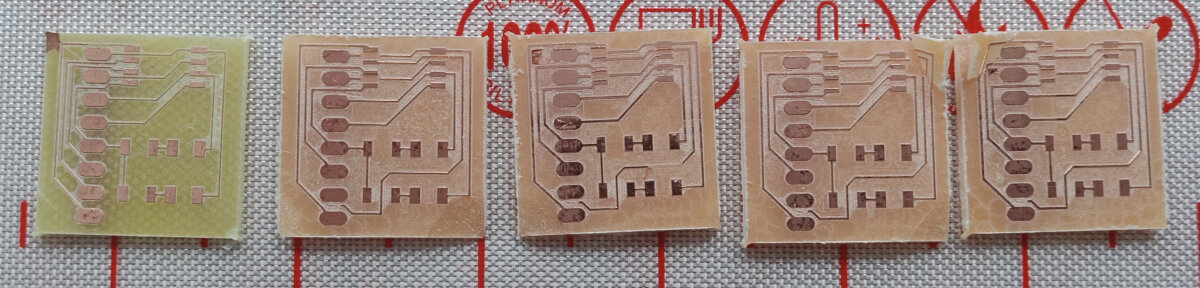 Milled pcbs: very
left: the first pcb with thin traces. Nevertheless, this was the best pcb of all we milled.
Milled pcbs: very
left: the first pcb with thin traces. Nevertheless, this was the best pcb of all we milled.
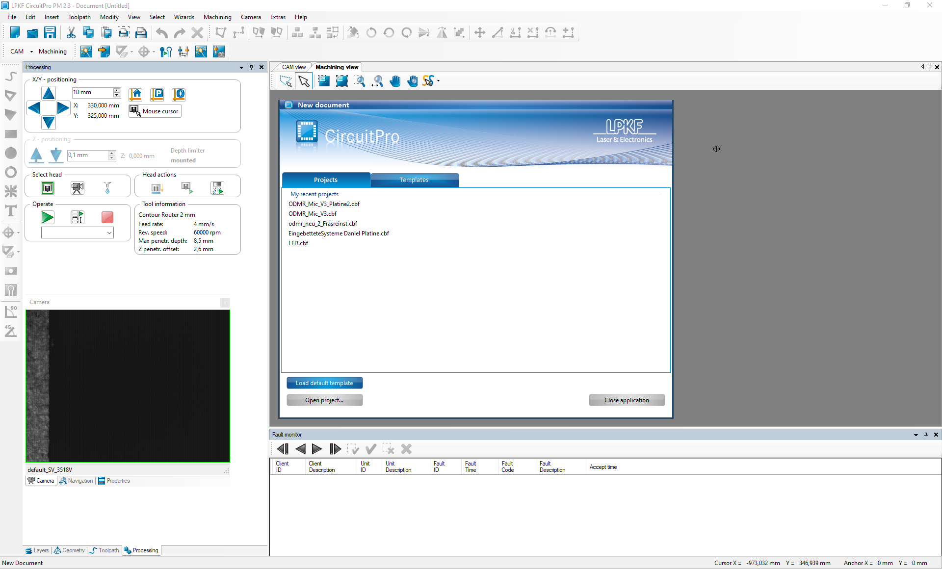
We use the LPKF CircuitPro programme to control the milling machine. We used the SingleSidedTop-template. Then we imported the Gerber-file. To to finalised...
Before soldering, I programmed the ATtiny85su using a SOP8 to DIP8 programming adapter for 200 mil microcontroller and an Arduino Nano used as programmer.
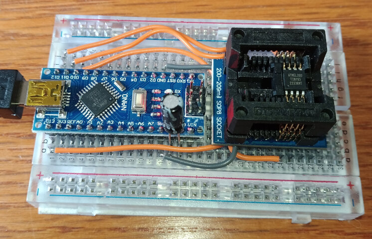
Arduino Nano used as programmer.
Then I checked if the written code was working using a breadboard.
The code should light up a WS2812b RGB led. The hue values should fade slowly.
The Arduino Nano only served as a power supply.
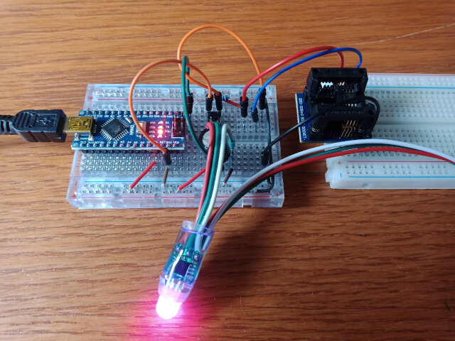
The code was working.
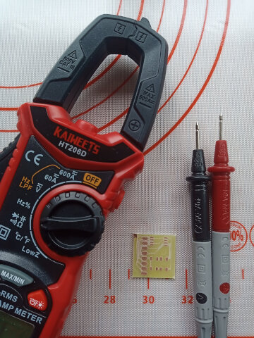
After checking that all needed traced on the pcb were working using a multimeter I soldered the components on the pcb.
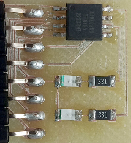
After soldering I took an image of the pcb with my smartphone to check the solder connections:
 Smartphone
image of my pcb. The solder connections look ok.
Smartphone
image of my pcb. The solder connections look ok.
Then I connected the pcb with all further components on a breadboard to see if my pcb was working – and: YES! the RGB led was lighting up in different colours, the power led was lit up and the status led showed the signal to control the RGB leds:
The Arduino Uno was only used as power supply.
As next step I wired the setup without the use of a breadboard.
I used an USB-hub as power supply and an USB-A connector with terminal blocks to screw in the cables for the power supply of my board and the WS2811 RBG led. Further, I connected the capacitor. With this setup you can control long chains of rgb leds. You only have to change the number of leds in the code and to be sure to connect an USB power supppy, which gives you enough power to supply all your leds. Here you see the RGB led slowly changing its color:
Here you can download the used code:
Instructions LPF
FIRST SWITCH ON THE MILLING MACHINE - THEN START THE PROGRAMME
Stick the circuit board to the sacrificial plate with masking tape on all sides in the marking. The masking tape should be about 10 mm wide and stick to the PCB.
In the first window click in the slider Templates - Single Sides Botton or Single Sided Top.
Click on these buttons one after the other from left to right up to the 7th button:
1) Magic wand: Process PCBs - Single Sided Botton or Top - FR4 – Done.
2) Load data: BoardOutline, BottomLayer/TopLayer, all drill files or TopLayer for Surface Mounted PCBs.
Assign files to the layers: Bottom to Bottom, Outline to Outline, all drill files to Drill Unplated.
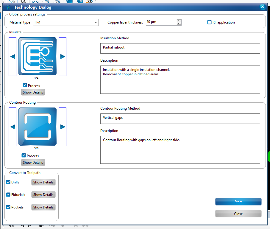
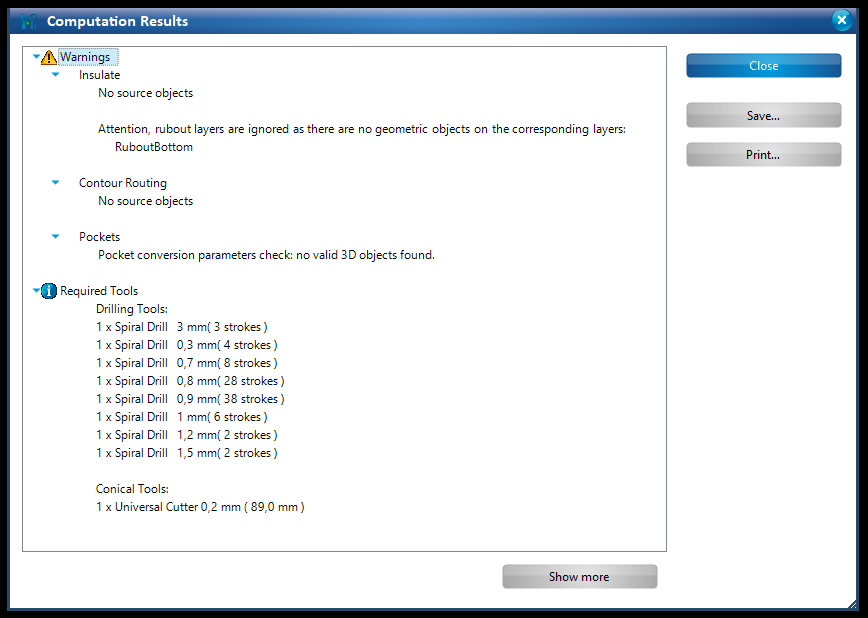
5) Technology Dialog: copper layer thickness: 50 µm, Insulation method: partial/full rubout, contour routing method: vertical gabs. START - next window: Close
6) Milling cutter: If necessary, add a missing mill - if there is no free space, replace a milling cutter that is not needed. To do this, select the router and click on Drop Tool. Then place the cutter in the appropriate position by hand. Requires a little force. Color banderole is between the bars. Note the percentage usage of the mill you took out.
Here you find the color coding of our mills:
Universal and Micro Cutter: Orange
Spiral Drill: Green
End Mill: Purple
Contour Router: Yellow
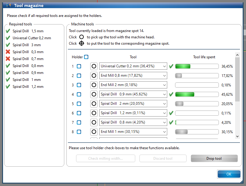
In this window: DO NOT SCROLL WITH THE MOUSE KEY - otherwise you will change the cutters!
The warning in the following window can be ignored.
7) Start the Board Production Wizard:
The display of the board only opens after clicking on the wizard.
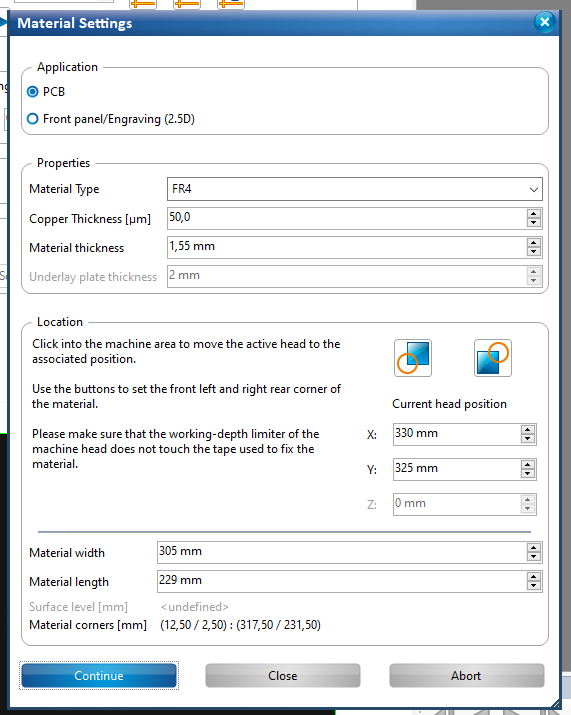
Material Settings: Continue
Placement: Position the board on the PCB. With Mouse cursor you can set the cutter to move where the mouse is. Check all 4 corners.
Position the geometry so that the aluminium housing around the cutter has clearance to all edges. Do not consider the masking tape, but the edge of the PCB, but you should not mill on the masking tape.
You can mill several PCBs at once. To do this, set the number of copies high. Enter 2 mm or -1 mm for spaces. This is faster as there are fewer tool changes and a better PCB utilisation. Then trace the corners of all geometries.
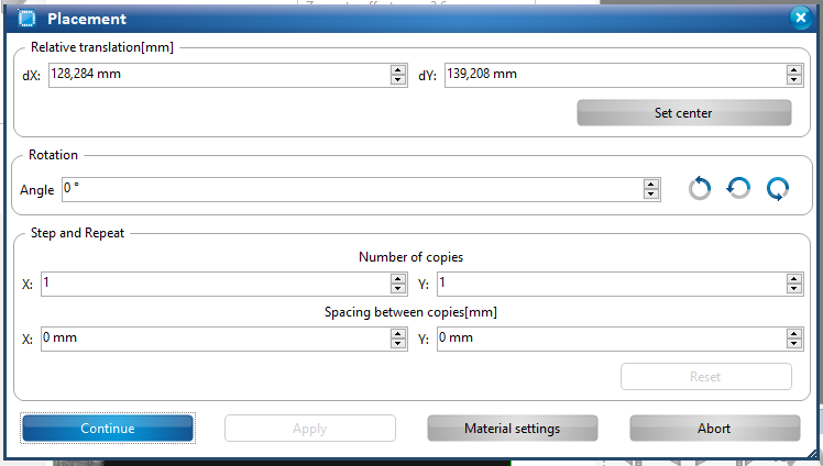
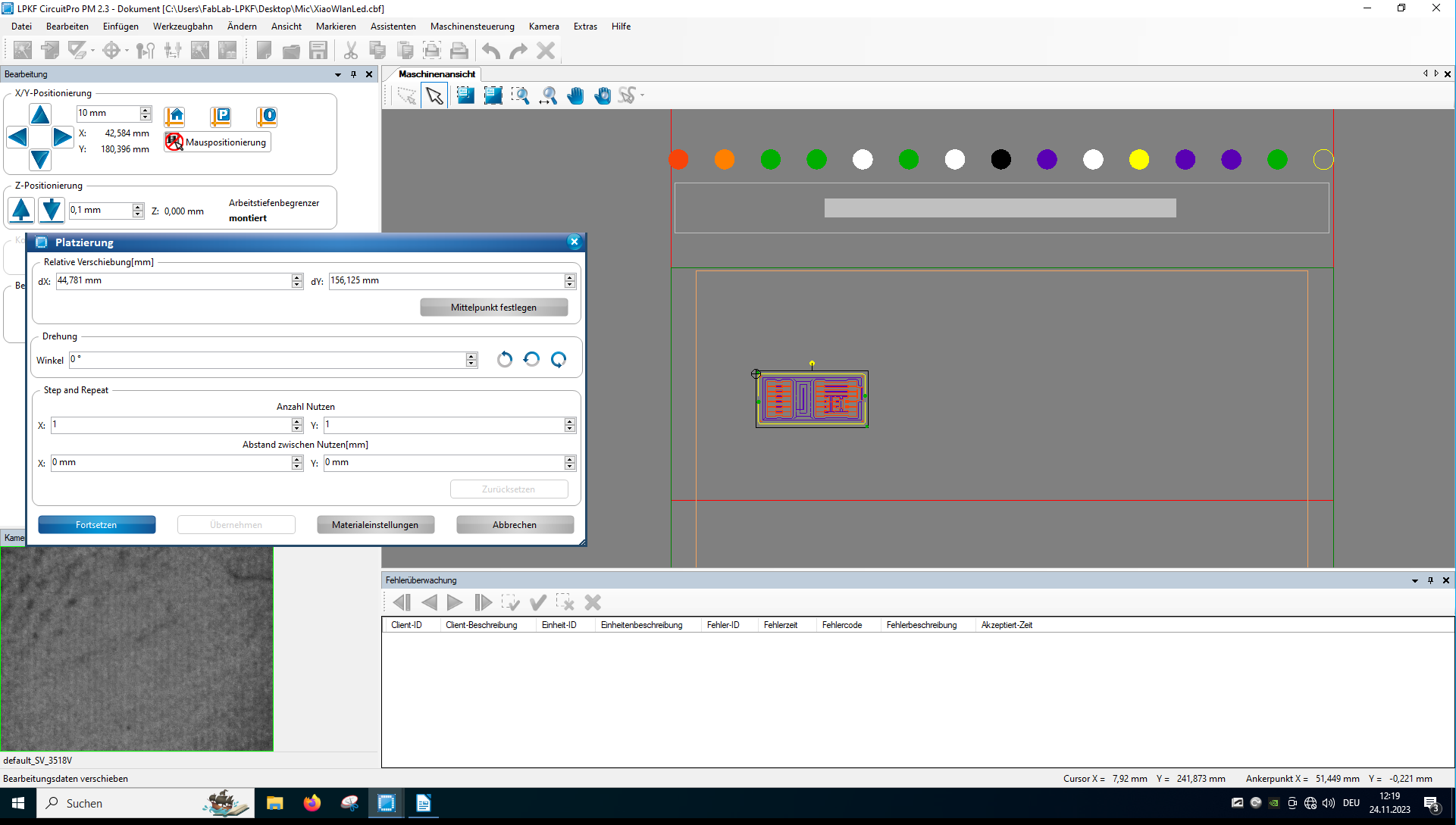
When mouse positioning shows a red circle with a line through it, the cutter moves to where you click with the mouse.
When you have positioned the board and click on Continue, milling starts immediately!
Milling didn't start once - it helped to put down the current tool and start again.
After milling: clear the sacrificial plate with a vacuum cleaner.
FIRST SWITCH OFF THE PROGRAMME - THEN MILL!
Group assignment
Here the design rules for our in-house PCB production process:
- Workspace: 229 mm x 305 mm x 35/22 mm
- automated tools: 15
- Finest details: 100 µm
- Rotational speed of the spindle: 60.000 rpm
-optical edge recognition to create two-sided boards
Feeds: The Milling Spindle is equal to 60,000 rpm and controlled by the software.
Speeds: The Drilling speed is equal to 120 strokes/min.
Material Thickness: 1.5 mm
Copper Thickness: 35 µm
Milling width adjustment: Automatic
Tooling: The Automatic tooling with 15 tool options:
Universal Cutter 0.2 µm – For cutting the board outline
End Mill 2 mm - mills the traces
End Mill 1 mm - mills the traces
Spiral Drill 2 mm - drills the start hole for the board shape
Contour Router 2 mm - rubout
Resolution (X/Y) - 0.5 µm
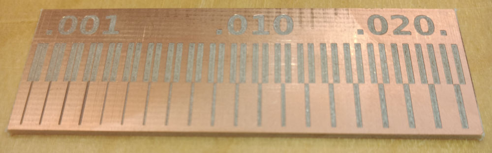
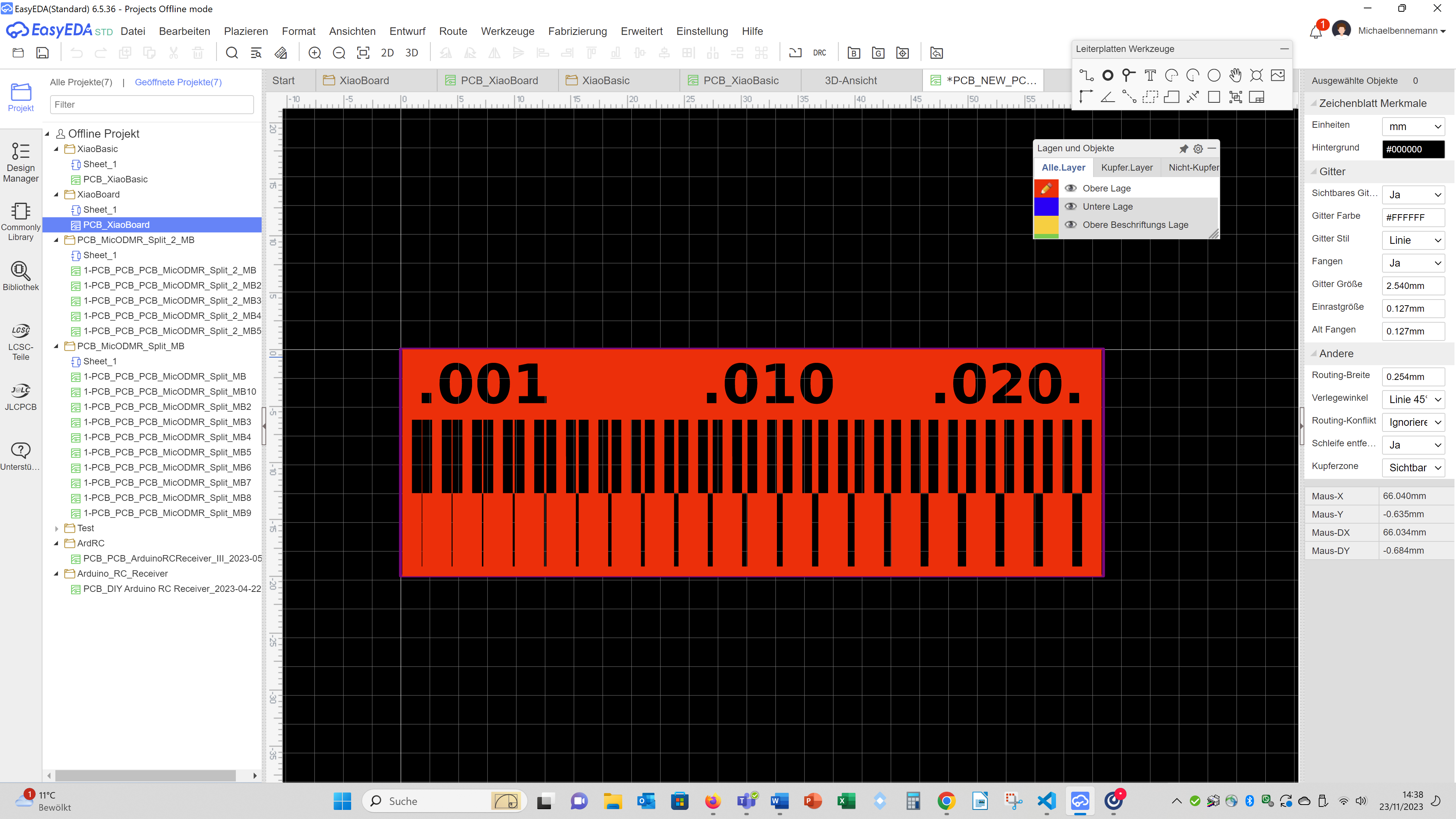
To test how fine our FPKF pcb milling cutter can mill we milled the test file Neil suppied us. To generate the g-code we imported the image in EasyEDA on the upper layer with the help of the image button (in the upper smaller window the last button right in the upper row).
Then we imported the top layer and the outline in the LPKF Circuit Pro Software.
The software chooses the mills itself.
The mills used the follwing mills:
Spiral Drill 1.5 mm
Universal Cutter 0.2 mm
Micro Cutter 0.1 mm
Sprial Drill 2 mm
Countour Router 2 mm
The result was quite successful: