Electronics production
Group Assignement: In-House PCB Production Process Design Rules
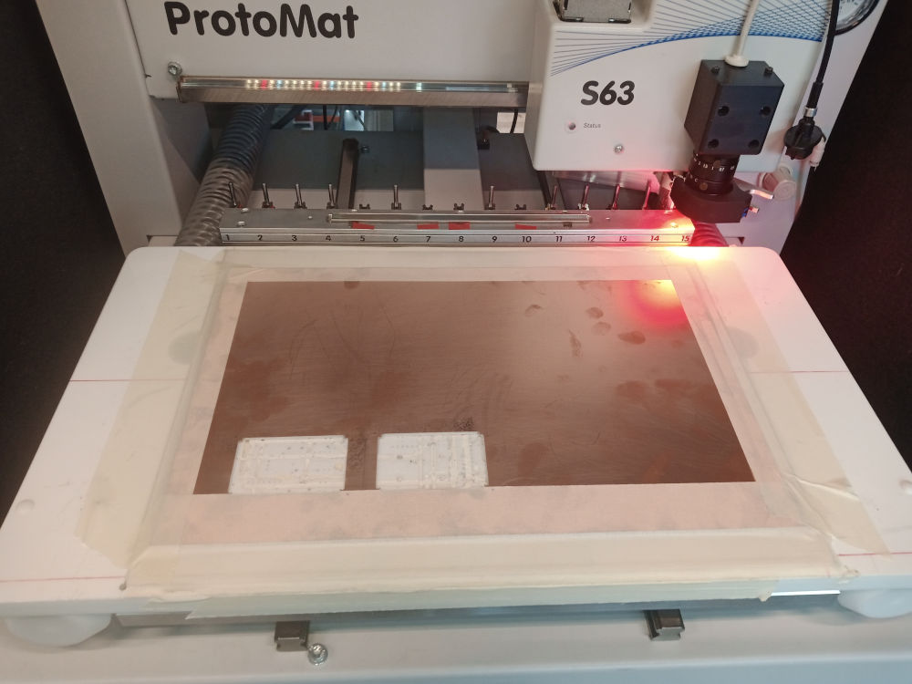
- Workspace: 229 mm x 305 mm x 35/22 mm
- Automated Tools: 15
- Finest Details: 100 µm
- Rotational Speed of the Spindle: 60,000 rpm
- Optical Edge Recognition for Two-Sided Boards
- Feeds: The Milling Spindle operates at 60,000 rpm and is software-controlled.
- Speeds: Drilling speed is 120 strokes/min.
- Material Thickness: 1.5 mm
- Copper Thickness: 35 µm
- Milling Width Adjustment: Automatic
- Tooling: Automatic tooling with 15 tool options:
- Universal Cutter 0.2 µm – For cutting the board outline
- End Mill 2 mm – Mills the traces
- End Mill 1 mm – Mills the traces
- Spiral Drill 2 mm – Drills the start hole for the board shape
- Contour Router 2 mm – Rubout
- Resolution (X/Y): 0.5 µm
To test how fine our FPKF PCB milling cutter can mill, we milled the test file Neil supplied us. To generate the g-code, we imported the image in EasyEDA on the upper layer with the help of the image button (in the upper smaller window, the last button on the right in the upper row).
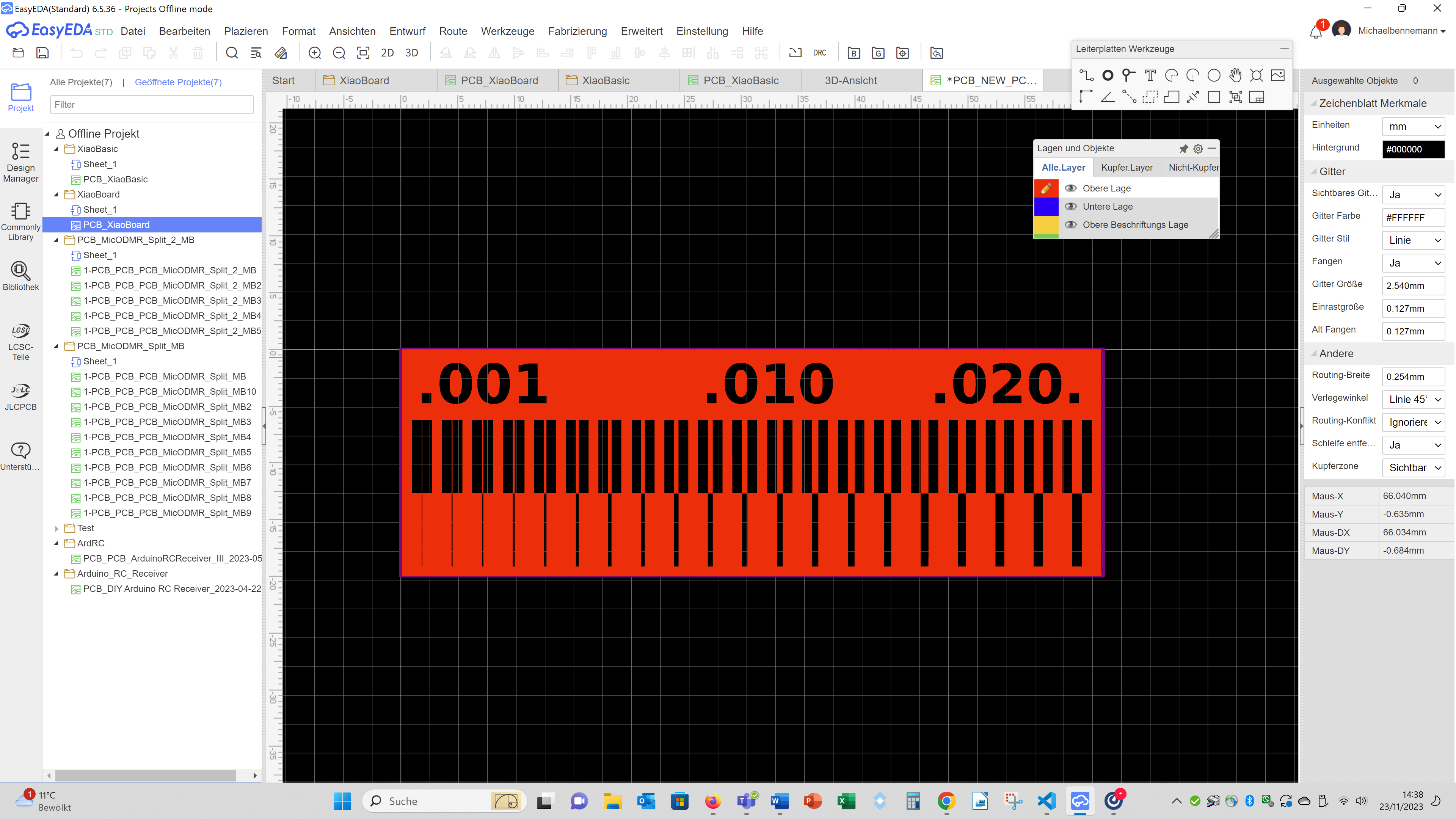
We then imported the top layer and the outline into the LPKF Circuit Pro software. The software automatically selected the milling tools, utilizing the following cutters: Spiral Drill 1.5 mm, Universal Cutter 0.2 mm, Micro Cutter 0.1 mm, Spiral Drill 2 mm, and Contour Router 2 mm. The outcome was quite successful

Group Assignment: Workflow for sending a PCB to a board house
Here is a detailed explanation of my part of the group assignment, which involves sending the PCB to a production house. This part complements the work done by Michael Bennemann.
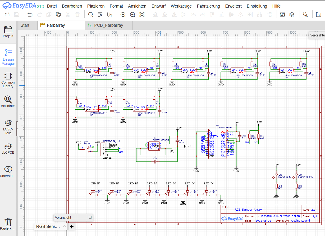
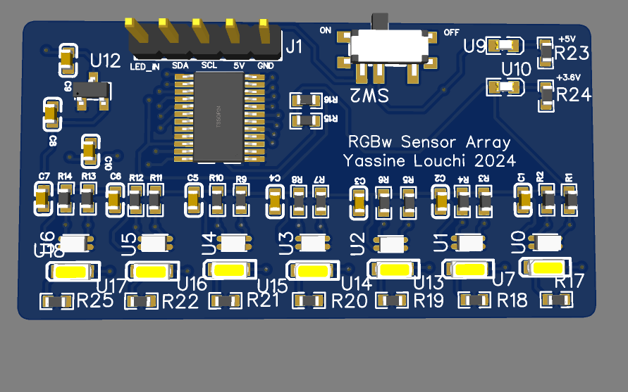
This board is an RGBW sensor array which will be used as a sensor for a robot so that it can follow color lines.
Creating a Schematic in EasyEDA
I began by designing the schematic in EasyEDA. This involved selecting the components and defining their connections to ensure the circuit works as intended.
Creating a PCB Design
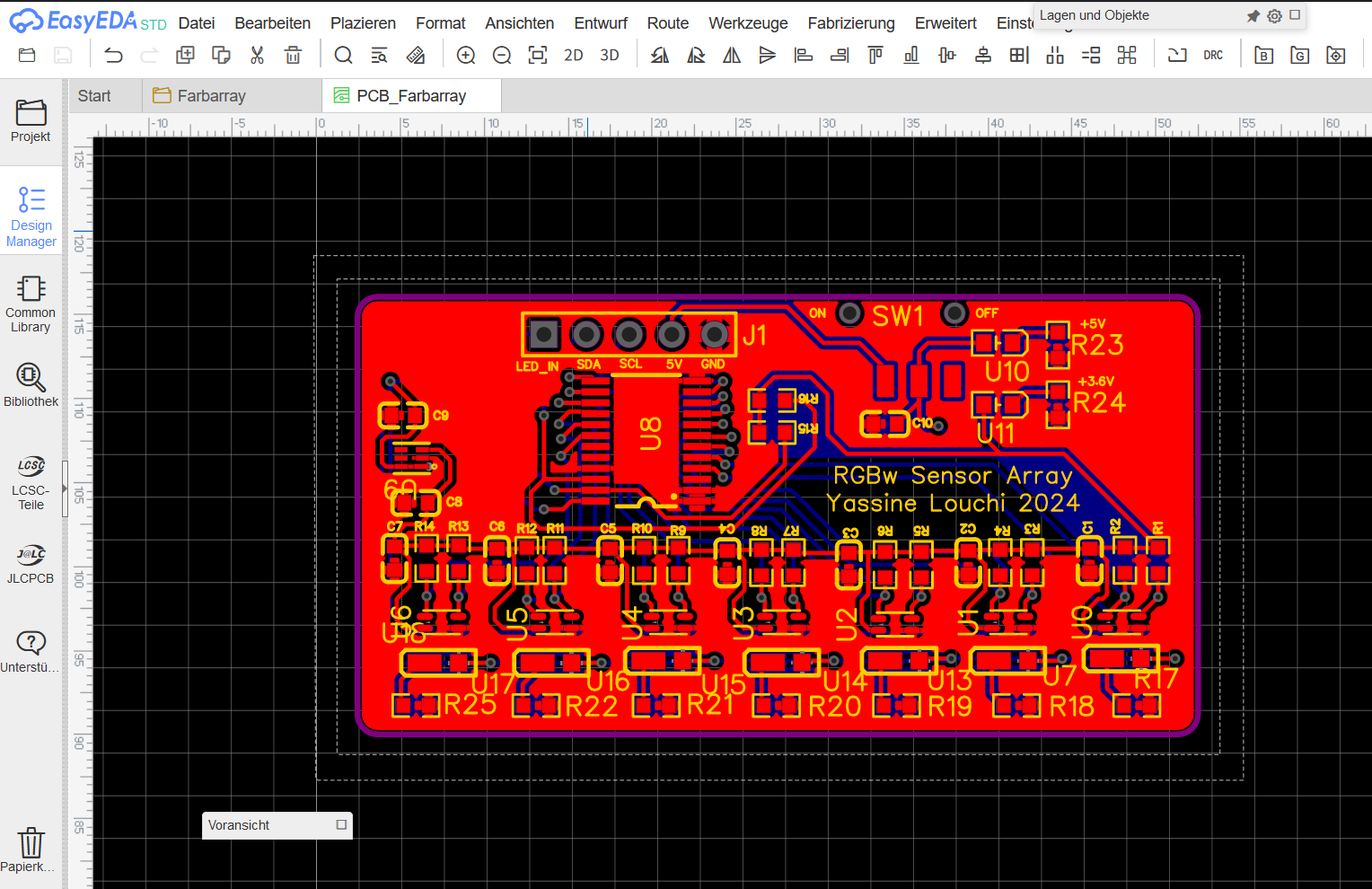
Once the schematic was completed, I moved on to designing the PCB layout. This step required careful placement of components and routing of traces to optimize the design for manufacturability and performance.
Generating the Gerber Files
After finalizing the PCB design, I generated the Gerber files. These files are essential for PCB fabrication as they contain all the necessary information for each layer of the PCB, including copper layers, solder mask, and silkscreen.
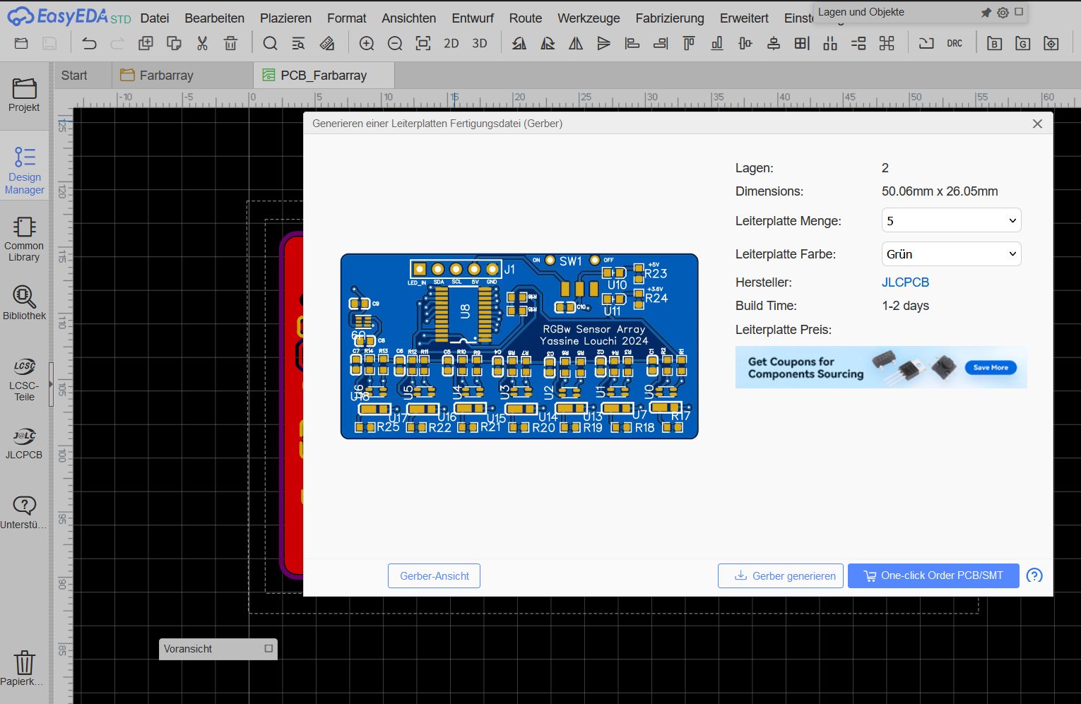
Loading the PCB on the Platform of the PCB Production House
I uploaded the Gerber files to the PCB production house's platform. This step involves selecting the appropriate specifications for the PCB, such as board thickness, material type, and finish.
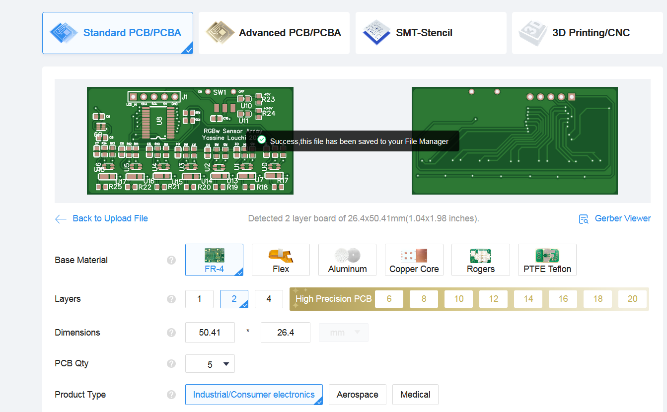
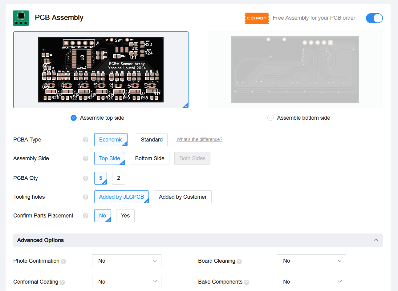
Exporting and Loading the BOM File
I exported the Bill of Materials (BOM) from EasyEDA and uploaded it to the PCB production house's platform. The BOM file lists all the components that need to be assembled and placed on the PCB.
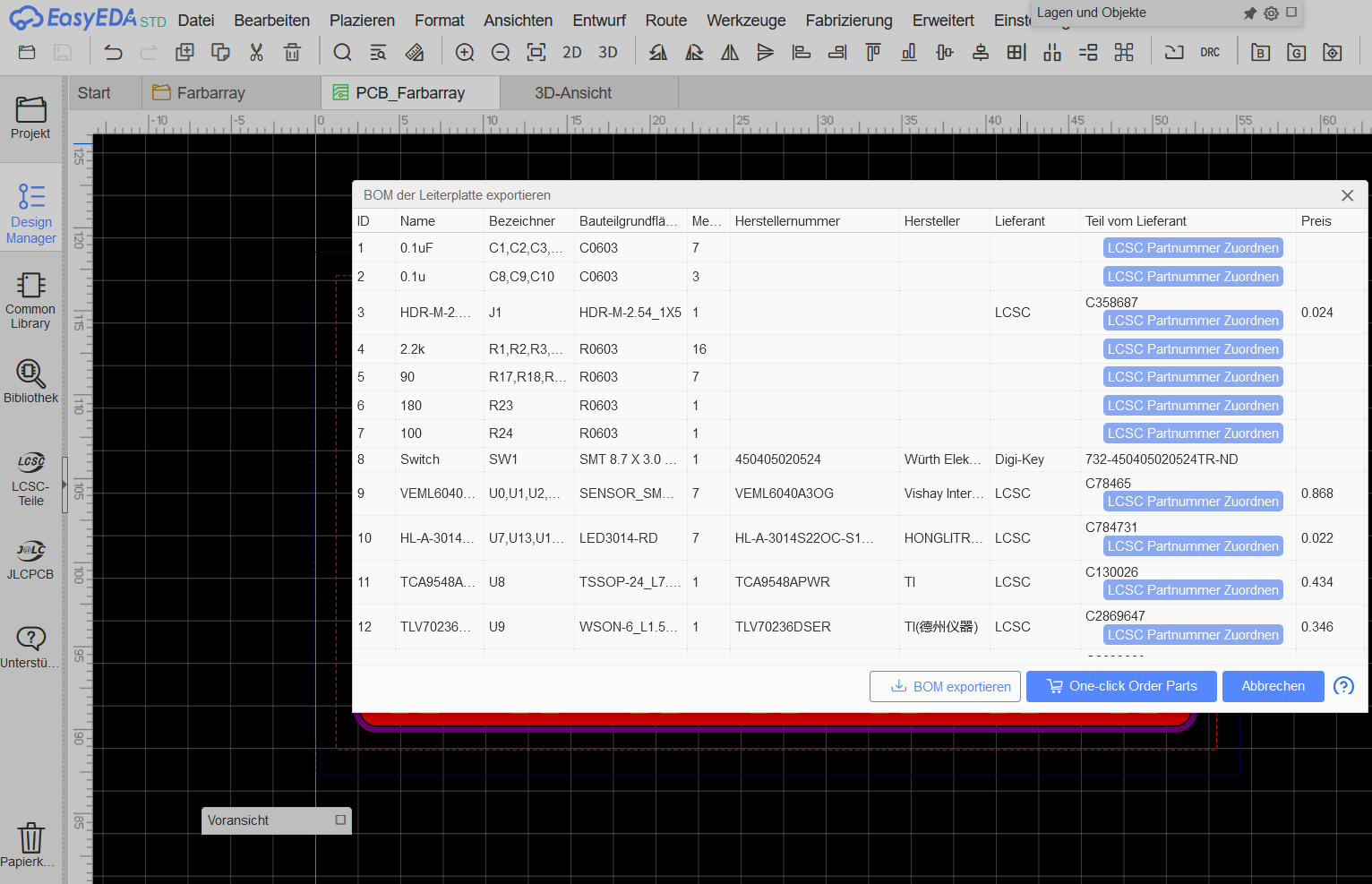

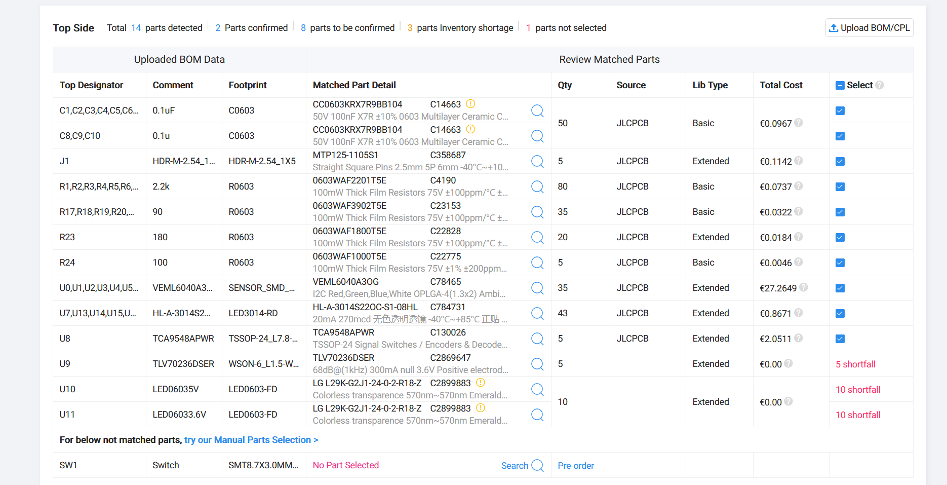
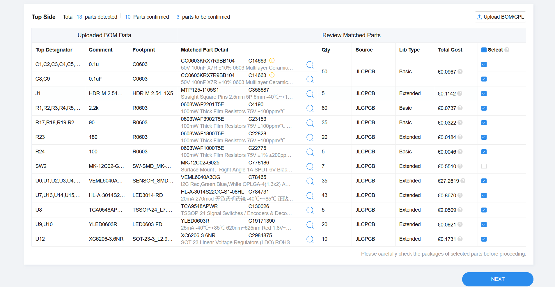
Checking for Availability of Parts and Replacements
After loading the BOM file, I checked the availability of all listed components. For any parts that were in shortfall, I identified and replaced them with suitable alternatives to ensure the assembly process could proceed without delays.
Final Board Design and Picture
I have later realized that 5V-PIN was not connected to the I2C_Mux that should control the RGBw-Sensors. I have corrected it and made a new production process.
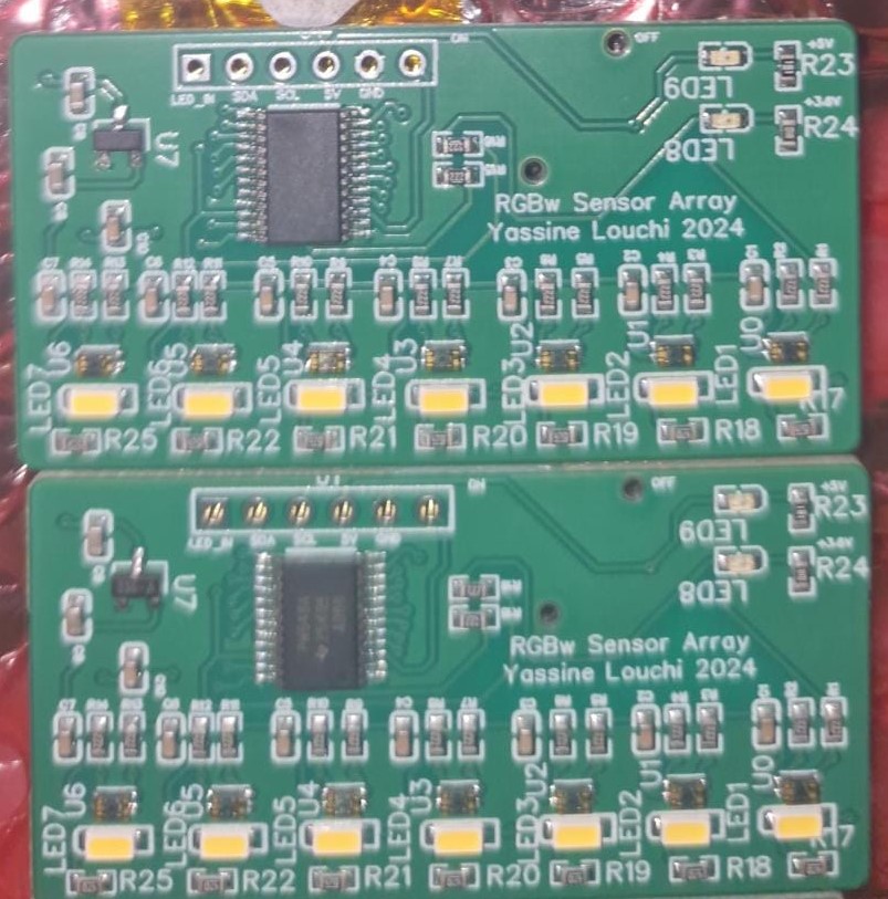
After completing the design and verifying all details, here is a picture of the final PCB design ready for production:
Note: This Board can be used under the Creative Commons-Licence: CC BY-ND 4.0
Please cite: © Yassine Louchi