WEEK 06: ELECTRONICS DESIGN
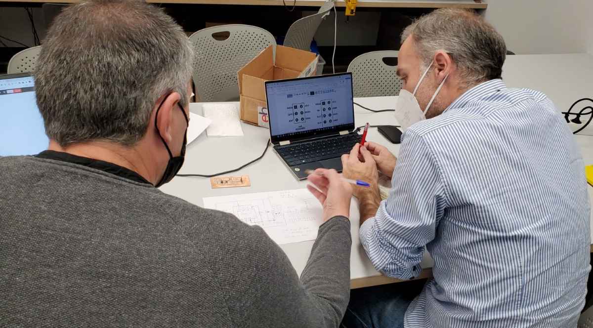
For this fourth group assigment, my "fabmate", Jon Merino, and I have to use the test equipment in our lab to observe the operation of a microcontroller circuit board. Here you can link to Jon Merinos grupal assignment as well. So, let´s start documenting!
- For this 5th week, we plan our time management for the goup assignment as follows:
- Document the equipment that´s available in ouf FabLab and test it with a functional board. In this case, we used one of the boards created by our instructor Alberto González.
- For the INDIVIDUAL ASSIGNMENT , my planning will be:
- Redraw an echo hello-world board adding a button and LED using EAGLE.
- Check the design rules and make it with the Roland Modela MDX-40A.
- Solder it and test it can communicate
GROUP ASSIGNMENT
TEST THE EQUIPMENT IN YOUR LAB
To start with this week´s assignment, we tested two different devices, a Tecktronic TDS 210 oscilloscope, and a KOBAN KM838 MULTIMETER.
TECKTRONIC TDS 210 OSCILLOSCOPE
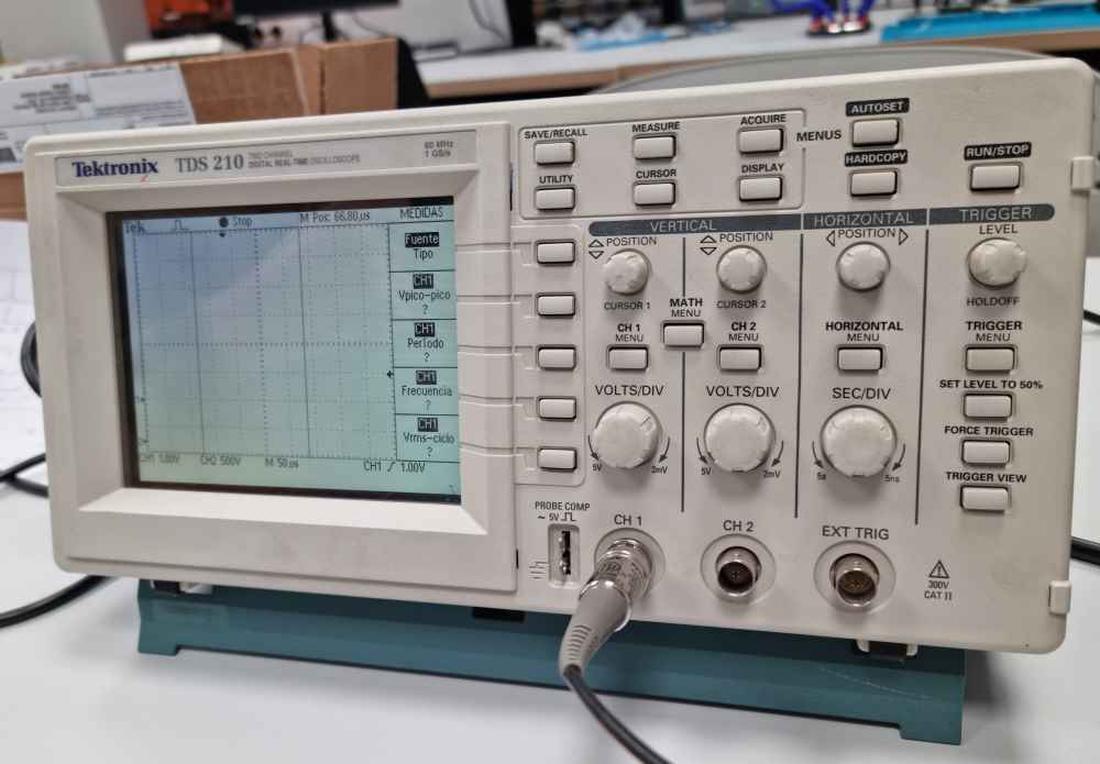 Tecktronic TDS 210 Oscilloscope
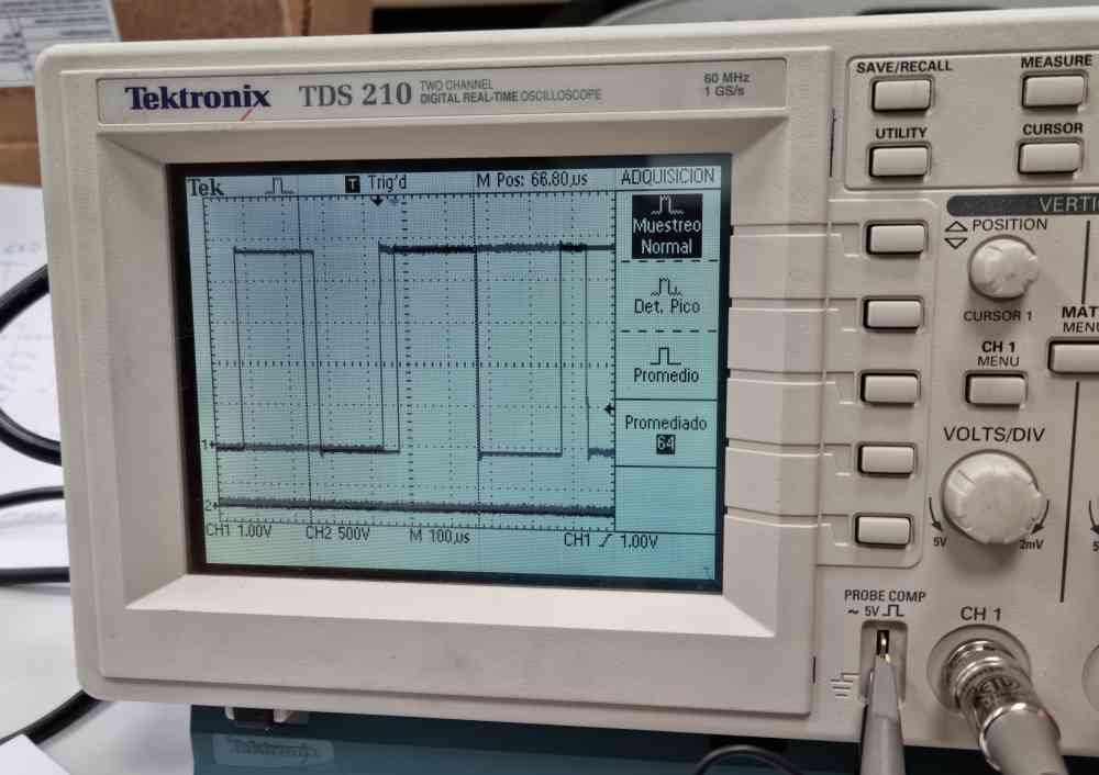 Probe comprobation
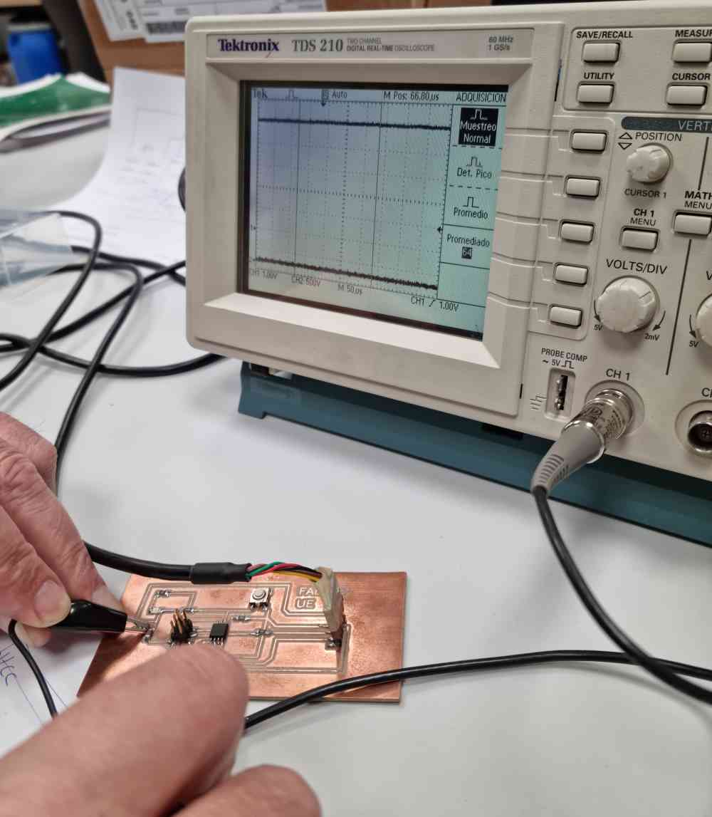 Measuring voltage in PCB
I´m very lucky to share my fabacademy experience with my fabmate Jon Merino, a engineer with experience in electronics that can help me jump into the electronic design world in an practical and easy way. We started by using the Oscilloscope to measure voltage in a fuctional board, so we reviewed how it displays a voltage/time graph and how that graph has divisions, being each division 1 volt. Afterwards, we set our vertical (voltage) and horizontal (time) values and configured our trigger, which is the value were the measure starts. This measure is done with a probe, whose value can be attenuated by up to 10X.
Here you can check the Tecknotronic TDS 210 Oscilloscope data sheet.
KOBAN KM838 MULTIMETER
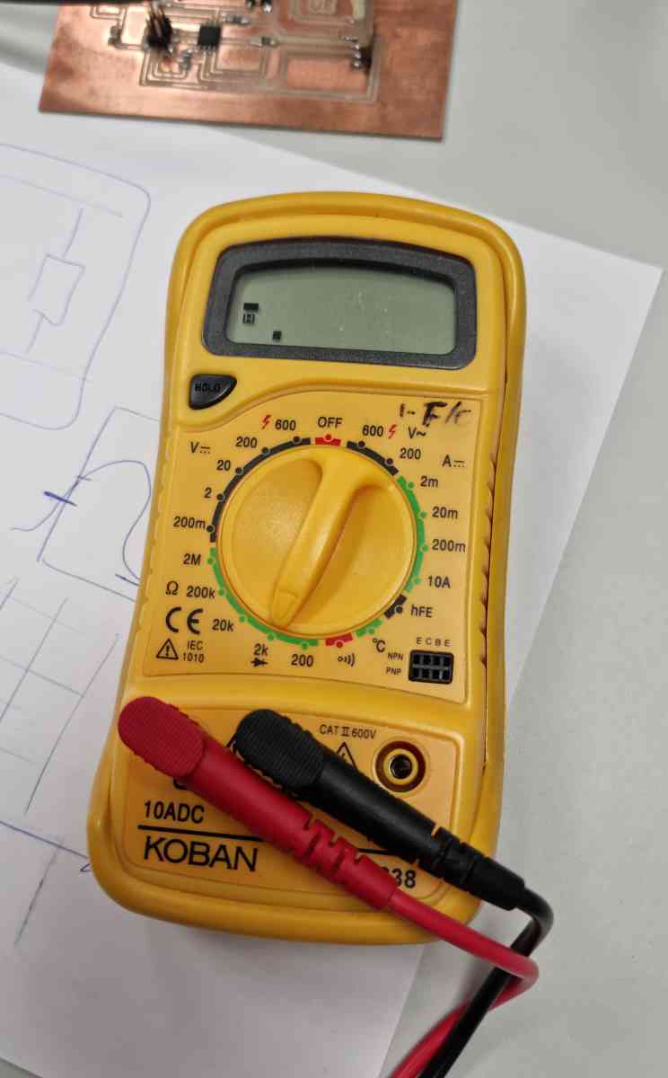 Koban KM 838 Multimeter
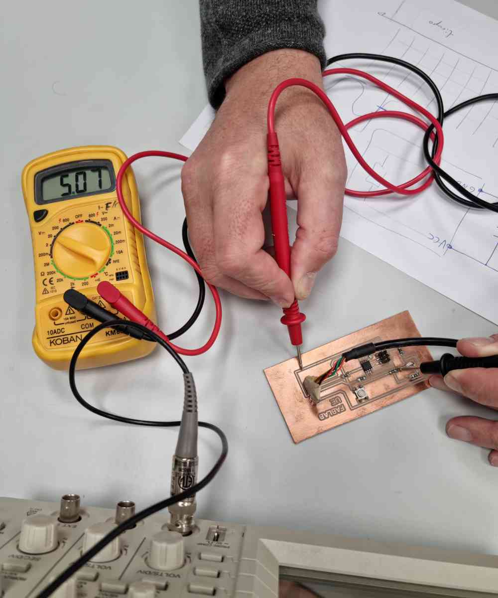 Measuring voltage
Once practiced with the oscilloscope, we used a Koban KM838 multimeter, in this case, it´s a very simple multimeter with DC and AC current measurement, so we just practiced its usability in the board with voltage and diode testing. I tried to find the data sheet, but it seems that is an old version that´s not longer available.
INDIVIDUAL ASSIGNMENT
REDRAW AN ECHO HELLO-WORLD BOARD
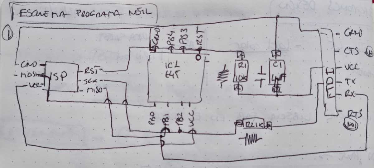
This weeks seems that it´s going to be a little bit more challenging than the weeks before because, besides of having 0 background in electronics, I have the feeling I need to invest time in understanding the whole process first. Luckily my "fabmate" Jon Merino has experience so we reviewed camly all the components and design rules of Neil´s ATtiny45 board.
DATA SHEETS AND COMPONENTS LAYOUT
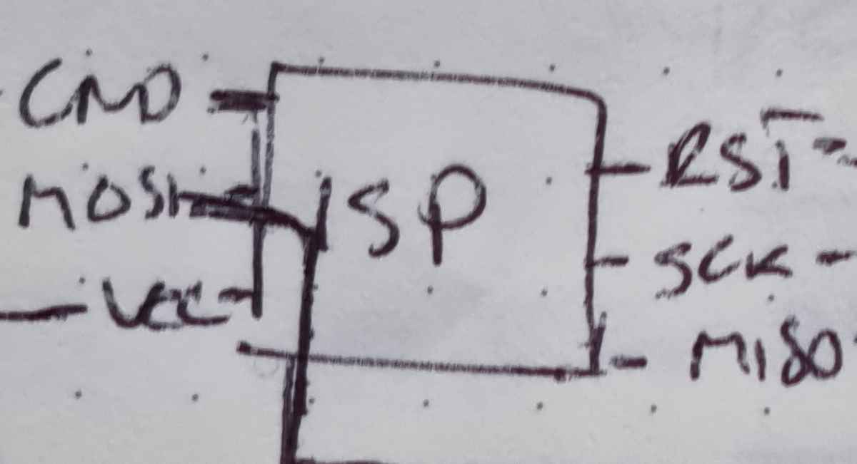
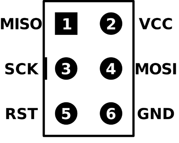
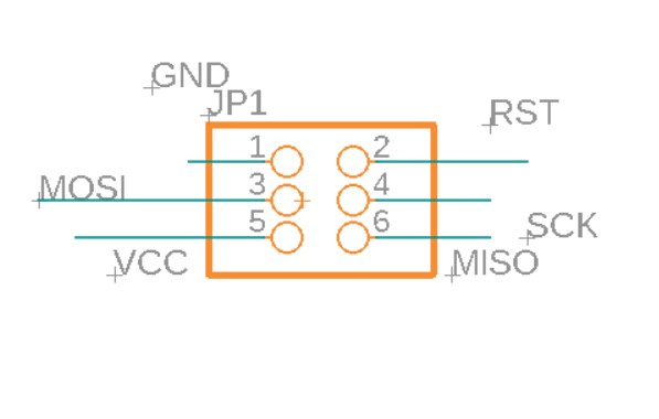
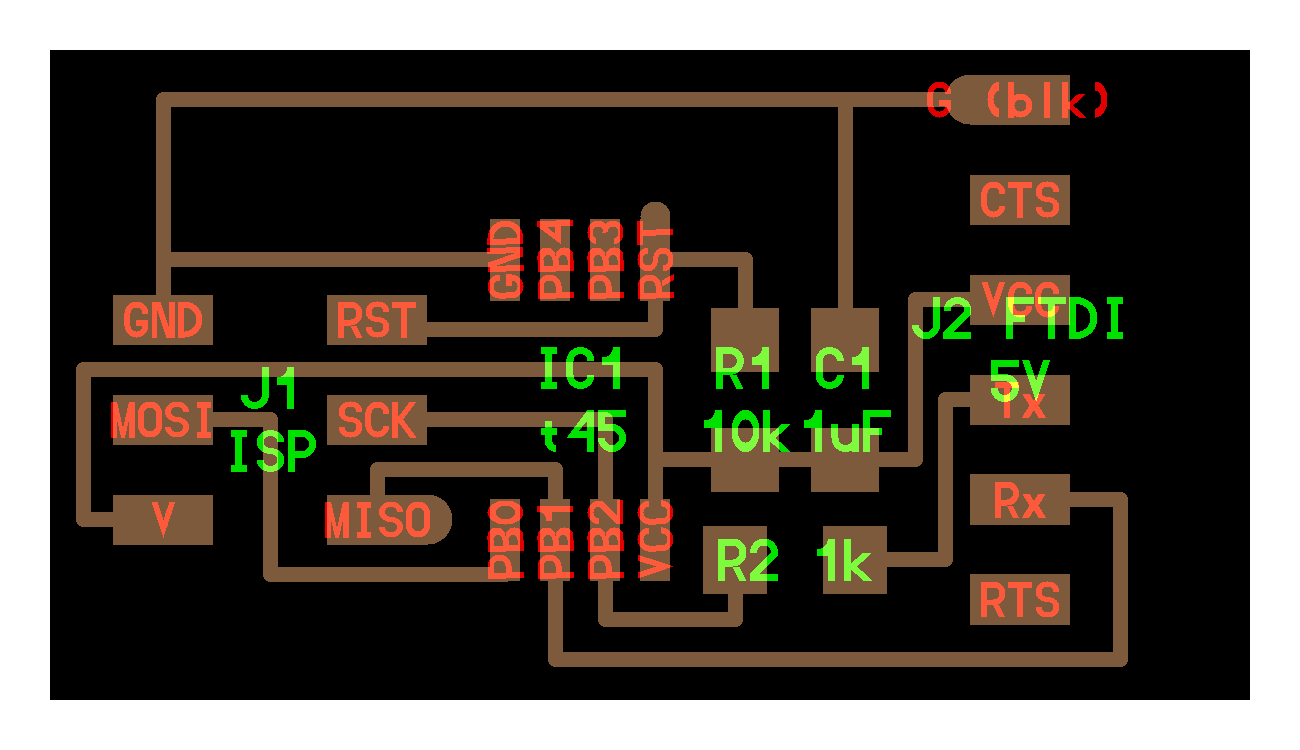
ISP DESCRIPTION
- MISO: Master In Slave Out.
- MOSI: Master Out Slave In.
- SCK: Clock. Is constant, to set the pace.
- RST: Reset.
- GND: Ground.
- VCC: Voltage Common Collector.
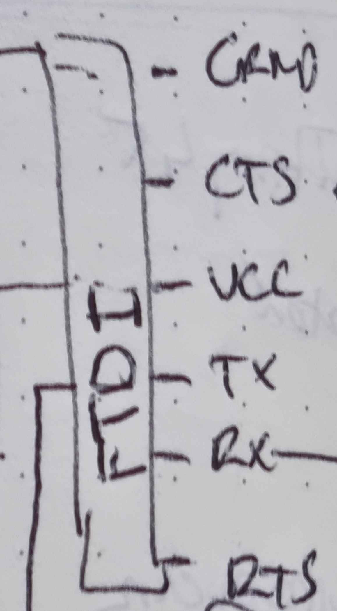
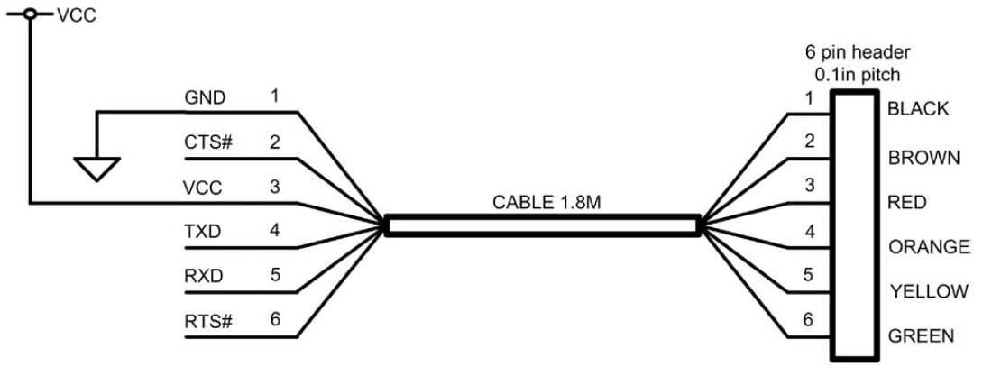
FTDI DESCRIPTION
- CTS: Clear To Send (Handshake signal).
- TX: Transmission data.
- RX: Reception data.
- RTS: Request To Send (Handshake signal).
- GND: Ground.
- VCC: Voltage Common Collector.
- Data Sheet.
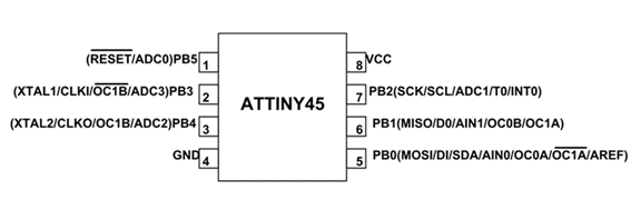
ATTINY 45 DESCRIPTION
- RST: Reinitiate communication.
- PB: Programable ports.
- GND: Ground.
- VCC: Voltage Common Collector.
- Data Sheet.
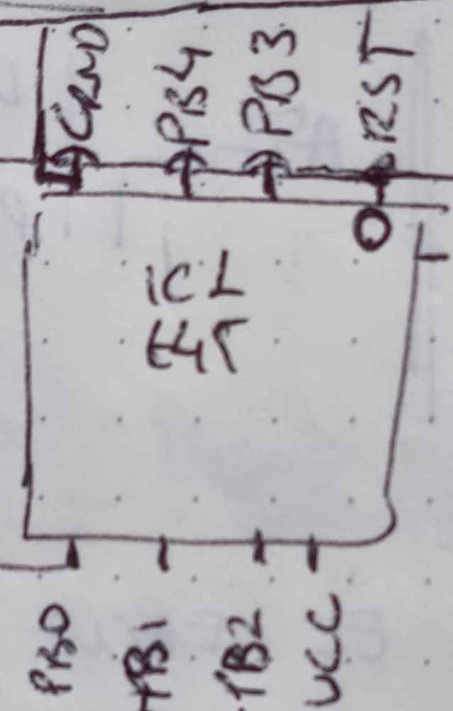
We also reviewed what capacitors, diodes and resistors were, because they´re components that were going to need. We found out this nice resistor code calculator that helps you to understand what a SMD resistor is, and helps you determine its resistance value. Once I had understood the role of each component, I prepared my board DESIGN RULES connections:
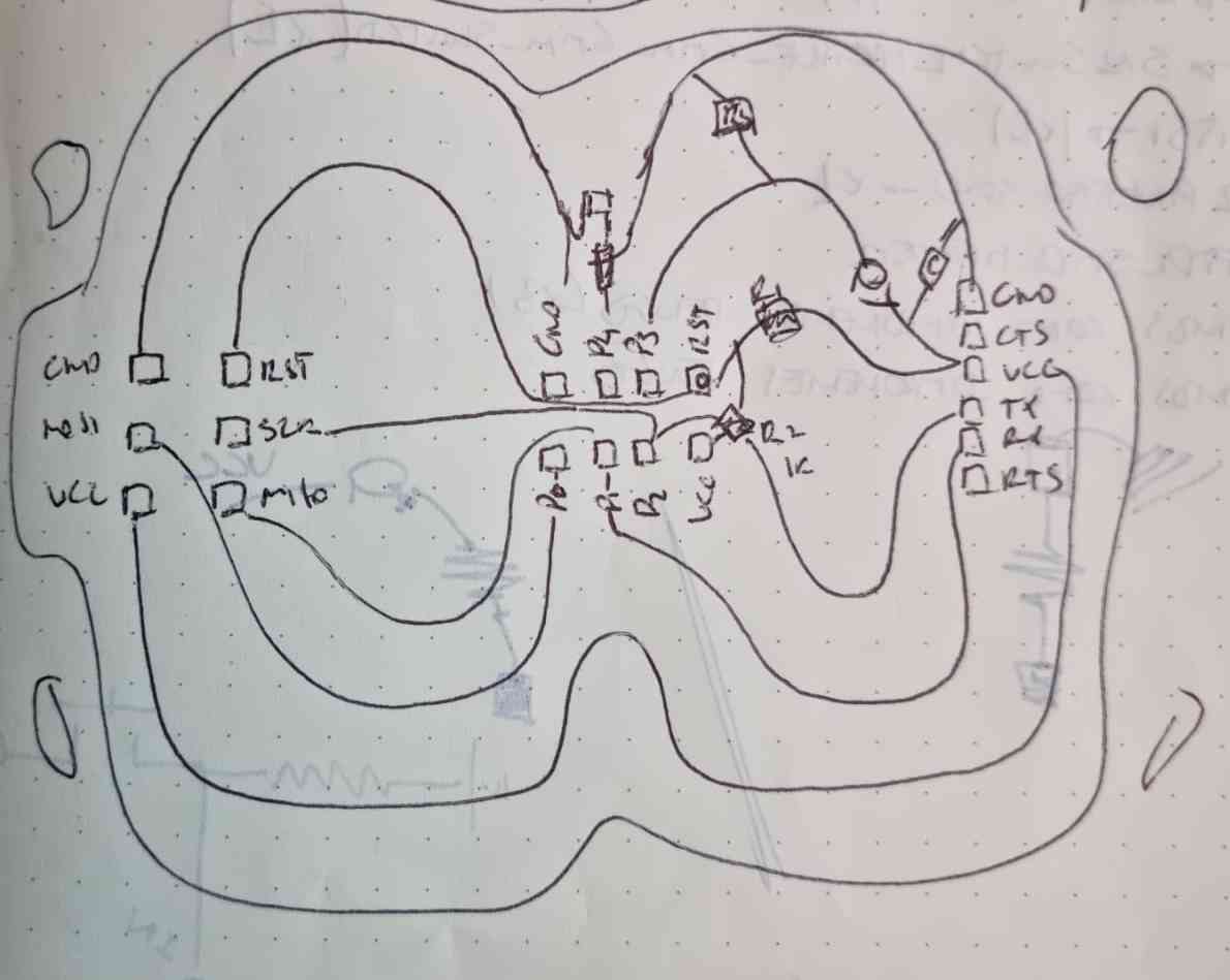
| PB0: Connected to MOSI(Isp). |
| PB1: Connected to Rx(Ftdi) + MISO(Isp). |
| PB2: Connected to Rx(Ftdi) + SCK(Isp). Adding a 1000k Resistor between PB2 and Rx (Resistors protects outputs and inputs). |
| RST: Connected to RST(Isp) + VCC(Ftdi). Adding a 10.000k Resistor between RST and VCC. |
| BUTTON: Connected to VCC in one side, and to PB3 and 4990 Resistor on the other side + GROUND. |
| LED: PB4 connected to 1000k Resistor + connected to LED + connected to GROUND. |
| CAPACITOR: Connected between VCC and GROUND to stabilize the power supply. |
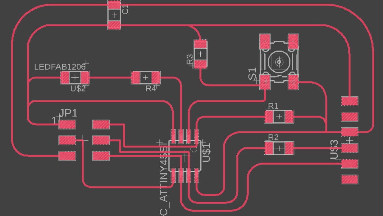
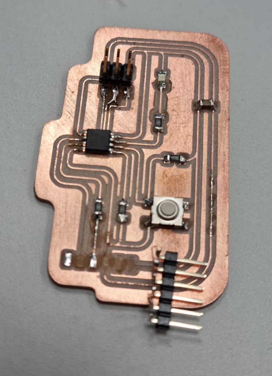
After having a first overview of all the components and design rules needed to redraw an echo hello-world board with a button and a led, I started designing a board that could be related to my area of knowledge (Healthcare). So, I tried to design a board based on the shape of a medular segment to give me extra motivation.
 Spinal cord cross-section for inspiration.
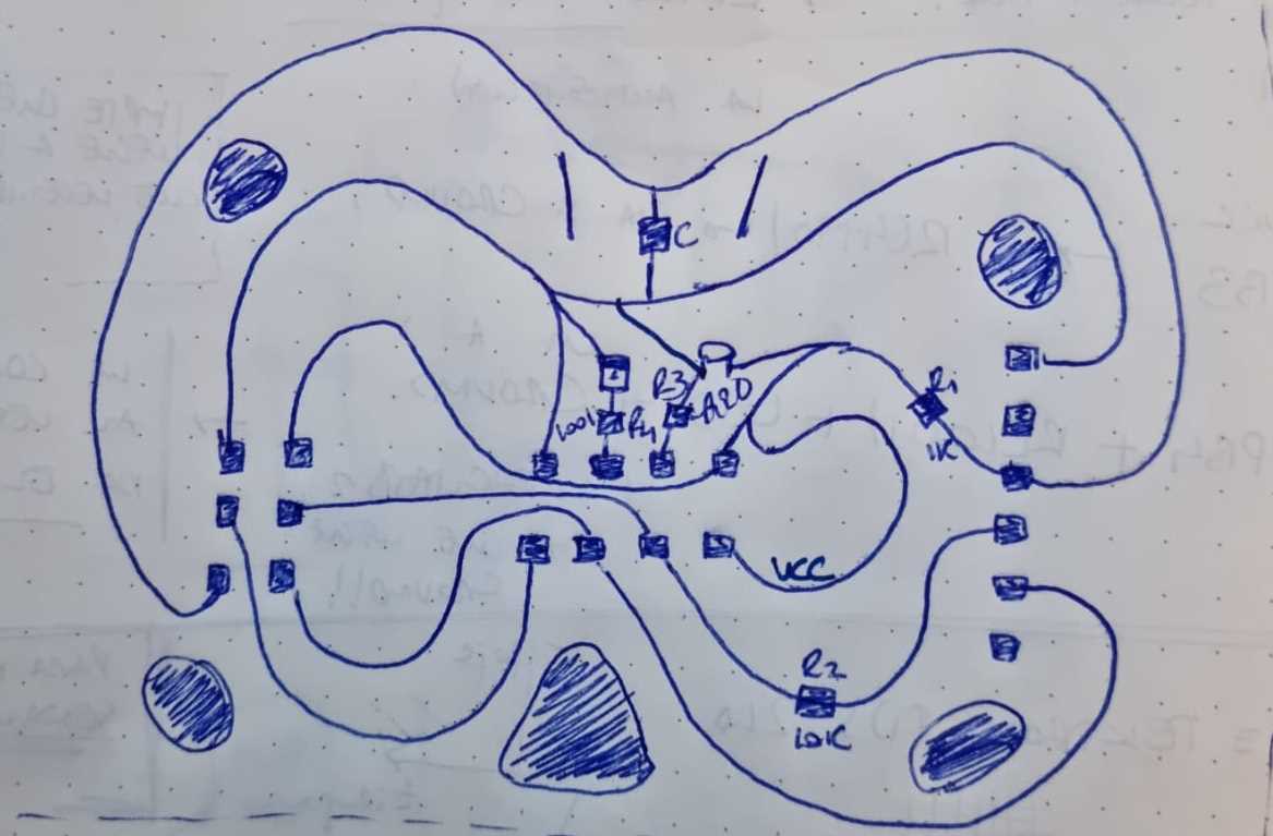 Schematic board design.
I have to say that I really enjoyed this part, It´s like a construction/designing game were you have to apply some mandatory design rules such as: avoid unnecesary bridges, stay away from conventional designs, etc.. So this is an example of what my first idea looked like.. The good thing about having 0 knowledge in designing your own board is that you´re not aware if it´s possible to design the electronics schematic later or not..!
DESIGNING WITH EAGLE
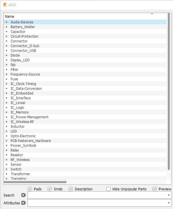
The selected software to redraw the echo hello-world board is EAGLE. A PCB design software that forms part of Fusion 360. To make it work properly we have to use a specific fab electronics component library for EAGLE (fab-eagle-library) from Fab Cloud, in order to make sure that the final design will be valid, and once we have loaded the fab library and the fab design rules,and we have listed the needed components, we can start our schematic.
COMPONENTS NEEDED
- Capacitator: CAP_UNPOLARIZEDFAB x1.
- Led: LEDFAB1206 x1.
- Resistors: R1206 x4.
- Switch: SW_SWITCH_TACTILE_6MM x1.
- UC_ATTINY45S1 x1.
- Connectors: 03X2PINHEAD-SMD x1, 06_FTDI_SMD_HEADER x1.
So, Alberto, our instructor, gave us some steps to follow, and we did the rest, and this is how it went:
| Download the specific EAGLE-fab electronics component library. And install it in the desired folder. |
| Go to Fusion -> Eagle -> Schematic Document: ADD fab library and select the specific components needed. |
| NAME (N) every segment of each component: If you name two segments the same, Eagle will "connect" all the segments that are named the same, so it will facilitate the PCB design afterwards. |
| Once you´ve got all the segments labeled, Go to PCB DOCUMENT. IMPORTANT! Load DRC/ERC fab RULES from eagle fab library installed earlier. |
| Now, route the segments as you´ve designed: In my case I did it manually and with bend traces mostly. |
| Once fully designed and routed you have to export it: Remember you can go back and foward between Schematic document and PCB document. |
| To EXPORT:Select the desired layer, go to the command line and write EXPORT, select IMAGE -> 1000dpi and Monocrome -> EXPORT as .png |
| Repeat it with the dimension layer: You will have to fill the inside of the dimension layer later with a paint program. I used gimp. |
| Now you´ve got your files ready to mill! |
 fab library.
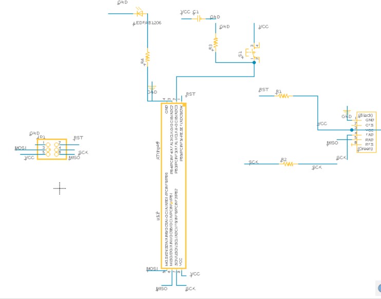 Schematic design components.
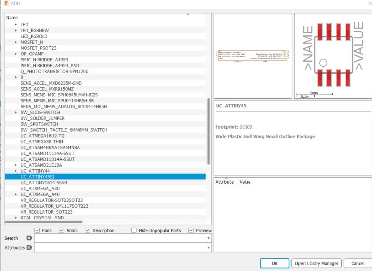 ATtiny45 component.
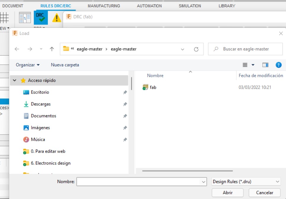 Eagle design rules.
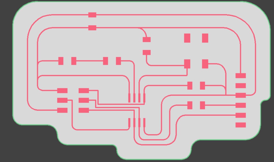 PCB with dimensions.
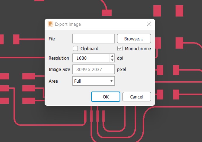 Exporting as .png image.
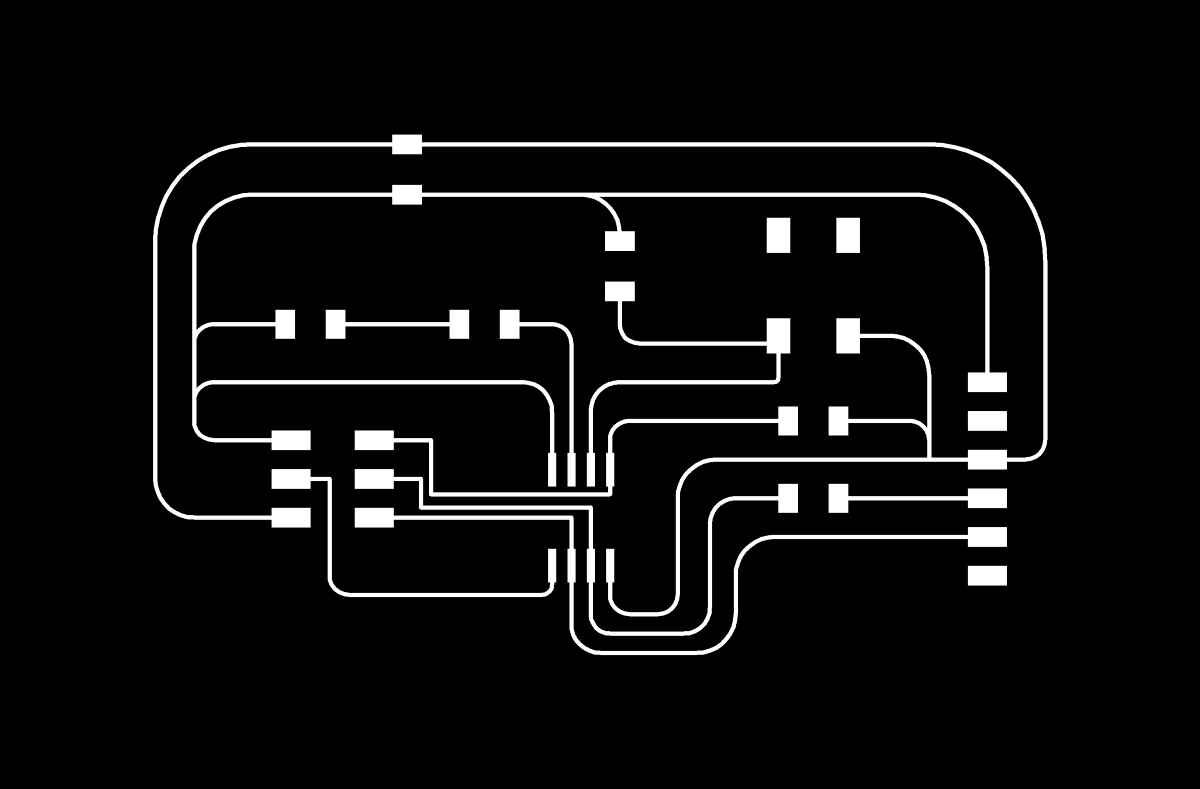 Inlines image.
 External image filled.
A couple of useful things that we´ve discovered by hard, and that they would have saved us a lot of time and wrongly milled PCBS are that, you can EASILY export your designs in .png format, as I mentioned above. You just have to write in the command bar EXPORT, and select your settings. It´s amazing how simple it is, and on the other hand it´s suprising how difficult is to find by yourself in EAGLE, thanks Jon Merino for that tip!. Another issue that gave me a huge headache (that´s the price to pay when you´re a newbie) is that you have to check not only that you have installed and running the fablab design rules (every now and then), but also that you have checked your traces width. Yes, I know this sounds obvious, but I didn´t know that the width was set to 10 by default.. My issues here were that luckily my first PCB was milled correctly with this small width, but I had to mill another one, and I just couldn´t get it right; broken tips, combed PCB´s, didn´t help either, but, despite that I really enjoyed the learning experience.
The final step with EAGLE was to push to 3D PCB that consists of visualizing in 3D your PCB in a fusion style. This step is quite easy. Go to Eagle, and switch to PCB document, once there, you can switch again to Push to 3D PCB (It only works if your´re in the PCB document). Once you select the 3D PCB desired option you will have a 3D design of your PCB opened in fusion, so, as in fusion, you´ll be able to view or not all the joints, sketches, boards, packages, etc..:
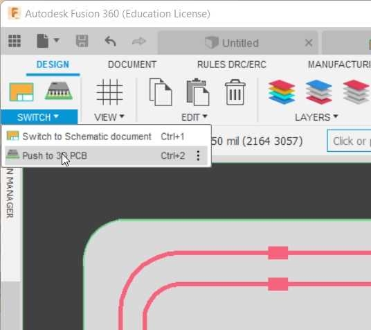 push to 3D PCB.
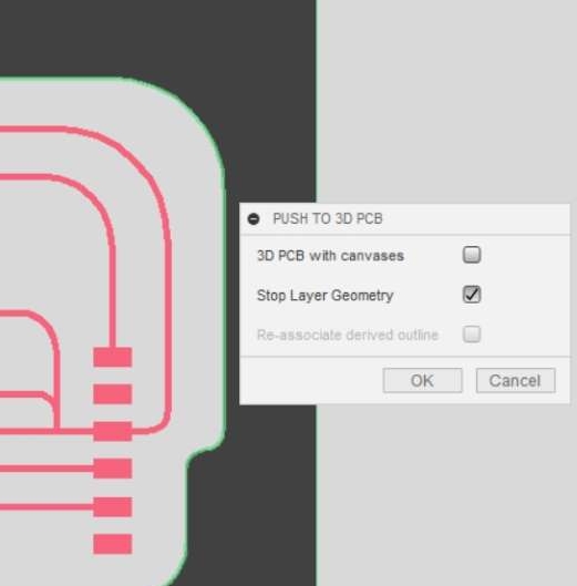 Select 3D settings.
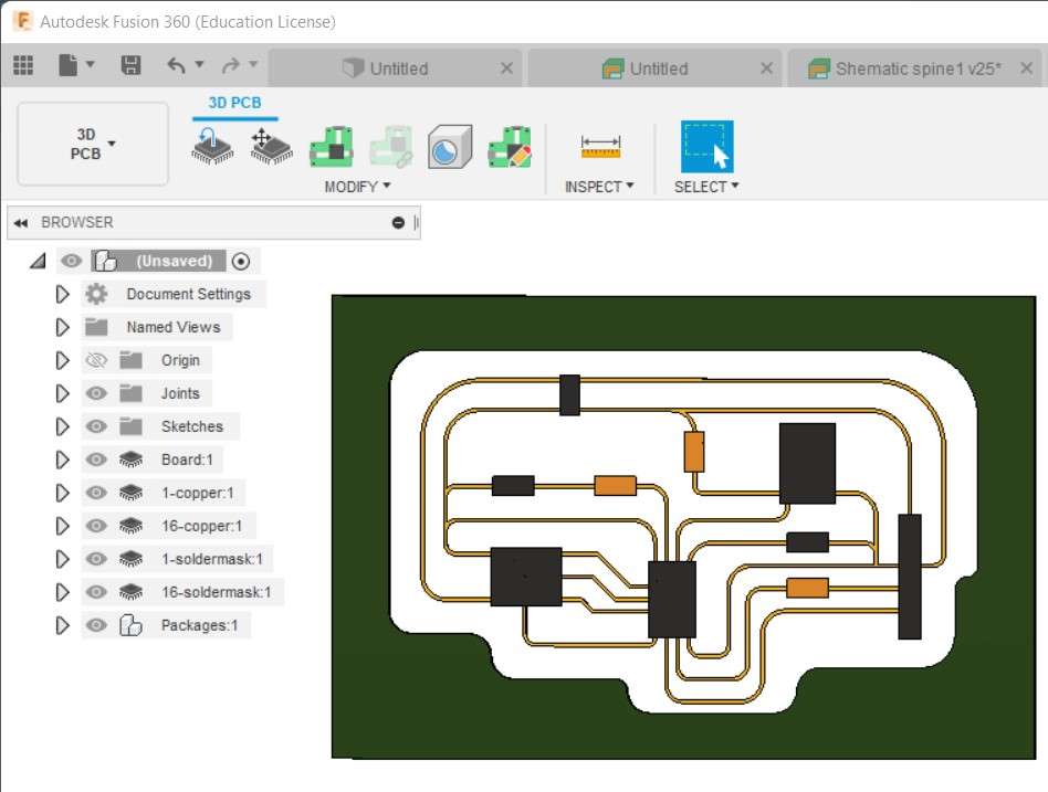 3D PCB design in fusion.
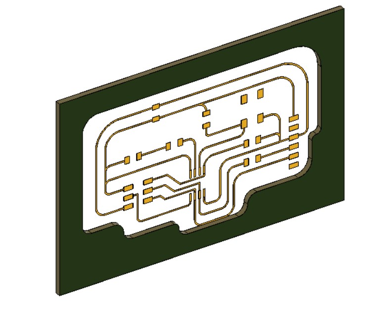 3D PCB.
As for thoughts about this experience, it was surprisingly entertaining and didn´t take as much time as I expected to work with EAGLE, but be cautious, you need to master what settings can make your milling rock or if not.. you can spend days trying to figure out why it just wont work properly.. But if you have that in mind and you´re fusion 360 friendly, EAGLE will be a great experience, and for sure i´ll be using it againg. But, in other hand, I wasn´t able, by now, to design my board with the design I wanted, too many curves.. But now it´s time to build our PCB.
Download eagle files: eagle schematics or eagle board.
BUILDING OUR OWN HELLO-WORLD BOARD
To create our hello-world board, we´re going to use the same workflow as the one describe in Week04: MODELA MDX-40A + PCB PRODUCTION PROCESS , you can check it if you want to know the complete workflow used, but in this case we will mill our recently designed board.
Download the .rml files created in ModsCE: Chana´s ModsCE internal.rml or Chana´s ModsCE external.rml
A couple of weeks ago, we had very little issues using our Roland Modela MDX-40A, so we had high expectatives this time too. At first, I had no issues preparing the file in ModsCE, but after a first try I had to modify the cut depth to make sure that the tip doesn´t break, because we had problems with brand new 0.4 tips that seemed quite long. So, the settings prepared for each file this time were:
- Tool diameter: 0.4mm
- Cut depth: 0.12mm
- Max depth: 0.17mm
- Offset number: 4
- Offset stepover: 0.5
- Speed: 4mm/sg
- Tool diameter: 0.6mm
- Cut depth: 0.2mm
- Max depth: 1.8mm
- Offset number: 3
- Offset stepover: 0.5
- Speed: 3mm/sg
As you can see in the following images, when modifying the inlines cut depth, at the first attempt, I went short (cut depth 0.7mm) and the board wasn´t milled properly, probably because apart of the cut depth it was combed, at the second attempt, after checking the FR1 PCB board and adjusting the settings, the result was good:
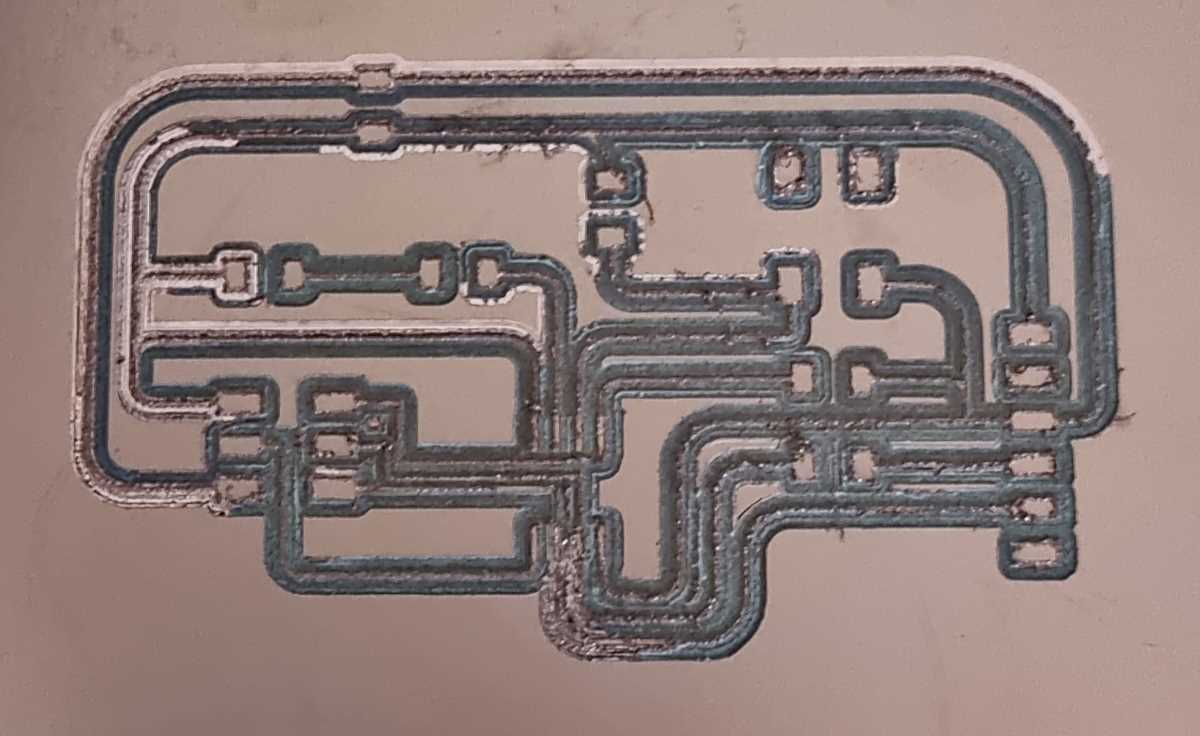 First attempt with low cut depth.
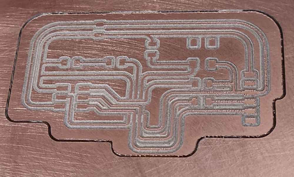 Final milling attempt.
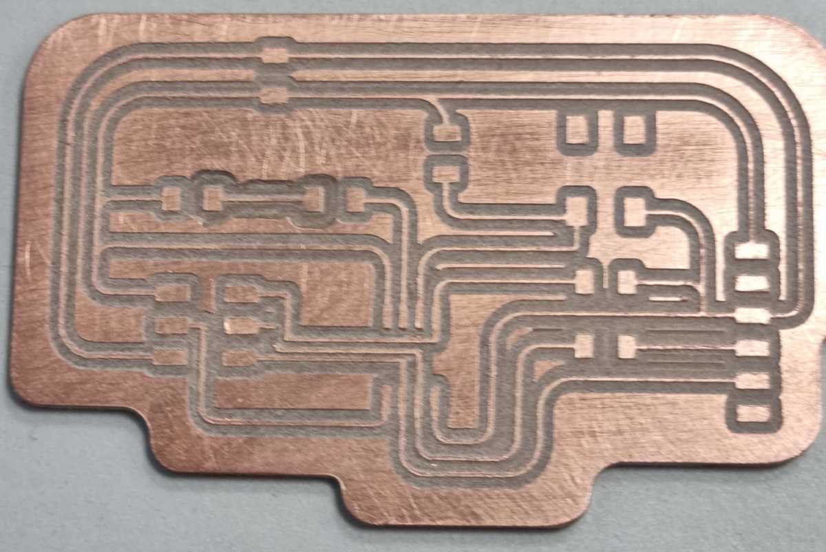 First PCB.
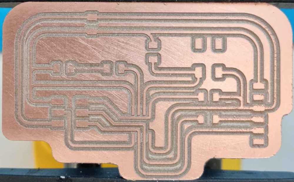 Final PCB.
SOLDERING
As for the soldering process, first we select and prepare our components, and afterwards I followed the same workflow as in week 04 Week04: Electronics design.
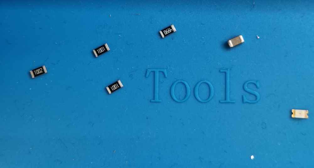
- 1x ATtiny45.
- 2x 1kΩ resistors.
- 1x 49Ω resistor.
- 1x 1000kΩ resistor.
- 1x LED.
- 1x green LED.
- 1x 2x3 pin header.
- 1x 6 FTDJ header.
- 1x Tactile 6MM swicth.
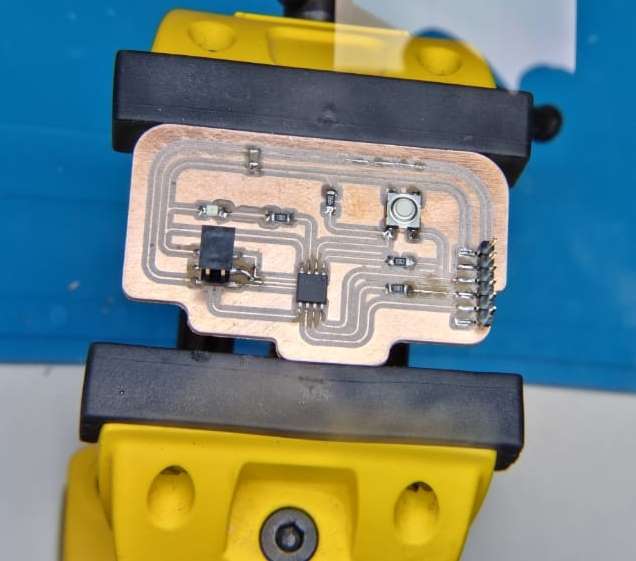
Regarding the soldering experience, I have to say it went pretty well, I changed the PCB holder from a flexible arm type to a rigid stable type (as you can see in the image below) and I felt much more steady. It also helped that my board is bigger than the programmer we soldered a couple of weeks ago, so I felt much more comfortable. I also warmed up a little bit by practicing in an old board and also used some steps that worked for me in my last (and first soldering) that were: heat up the iron un to 340ºC. Start with the microprocessor first as it´s in the middle, use a good magnifying lamp and a good pair of tweezers!
 Components for soldering.
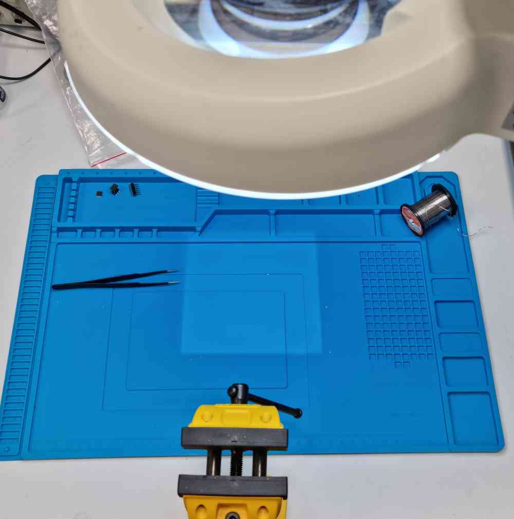 Soldering station.
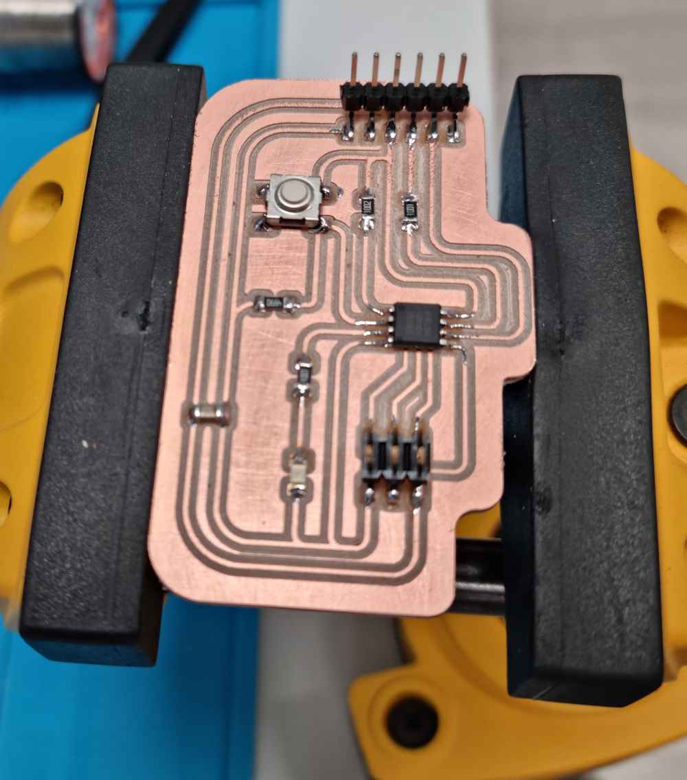 PCB finished.
Finally, I have to say that I was happy with the final result.., so, after soldering completely my PCB I went to the next step: Progaming the board.
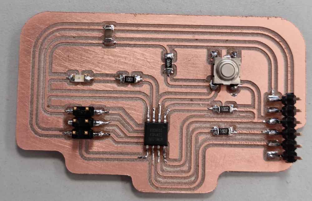 PCB soldered.
PROGRAMMING TO COMUNICATE
For this final part, I checked a couple of repositories to have a quick view of the process such as Alejandro Ausejo, which leads you easily on how to install the required libraries and settings, but we already had an experience a couple of weeks ago, because we had the opportunity to progam another PCB board with our programmers. First of all, you´ll need to have installed Arduino IDE, in my case I already had it installed, and it´s going to be the program i´m going to use to "talk to the board and to program it. So, this are the steps I made:
| Install and run Arduino IDE. |
| Connect our FabISP "programmer" with our new designed board with the 6 pin bus flat cable: Be careful and be sure that the cable is correctly connected with the ISP header. Check that the red line of the cable is on the side of ground. |
| Remember to connect them to your computer through a USB connector. In order to secure your computer. |
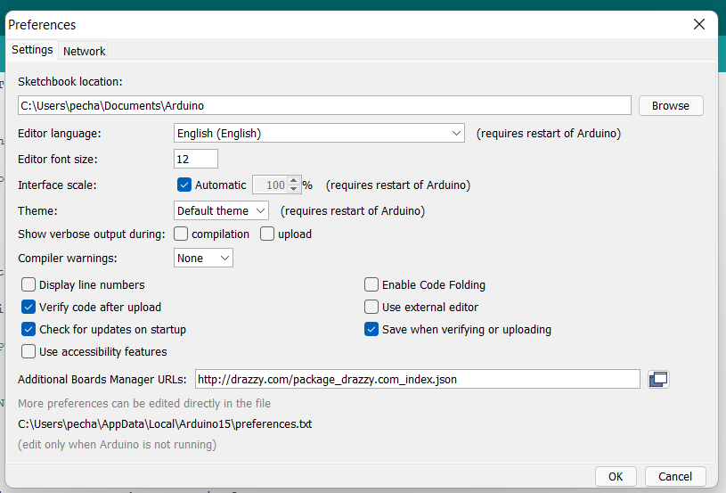
| Now you need to add an aditional board manager in IDE preferences: In my case I just followed Alejandro´s tutorial indications. |
| Go to Tools -> Manage libraries and search for ATTiny Core. Depending on your IDE version you´ll find different libraries. Any controlling ATTiny 45 (for our board) will do. |
| In Arduino IDE go to TOOLS, and set the type of micro and your specific characteristics. |
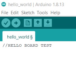
| Copy the hello-world board program of your microproccesor. Adapt it to your design regarding PB3 and PB4. In my case I followed Alejandro´s tutorial indications. |
| Paste it in arduino IDE -> New file. |
| Once all settings are done -> Go to SKETCH and UPLOAD using Programer. And hopefully your Hello-World board will be correctly programmed! |
 Adding aditional board manager.
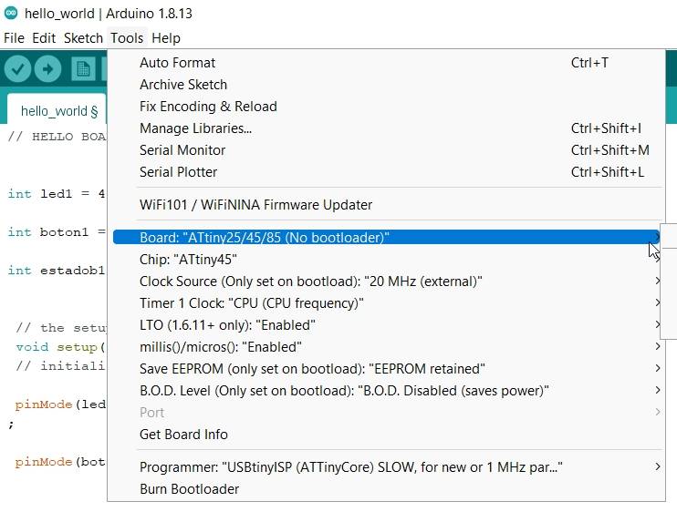 Search for ATtiny45 library.
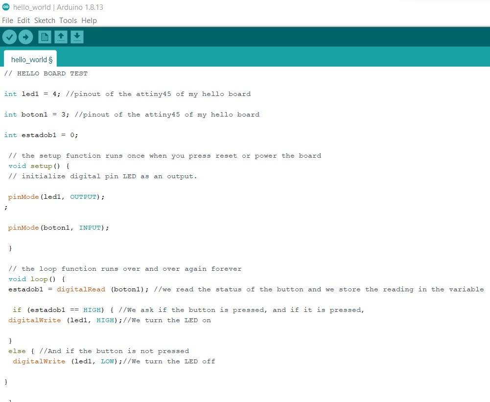 Hello-world program.
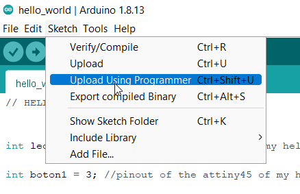 Upload using programmer.
And this is were the I suffer a fatal blow.. My FTDI is a little bit hard, and you have to press it to fit the pins, but this time, as I was trying to remove it.. it all came out together, the FTDI and the pins aswell, I literaly tore them from the PCB. I have to be honest (I won´t say I saw this coming) but I wasn´t expecting that it would work at the first attempt! Even do it would have been a blast to get it working!
 Problems with the FTDI!.
So I had to do another PCB, as it´s explained during the repository and finally was able to do a completely funtional PCB capable of comminicating, so another spiral done! Here you can check it!
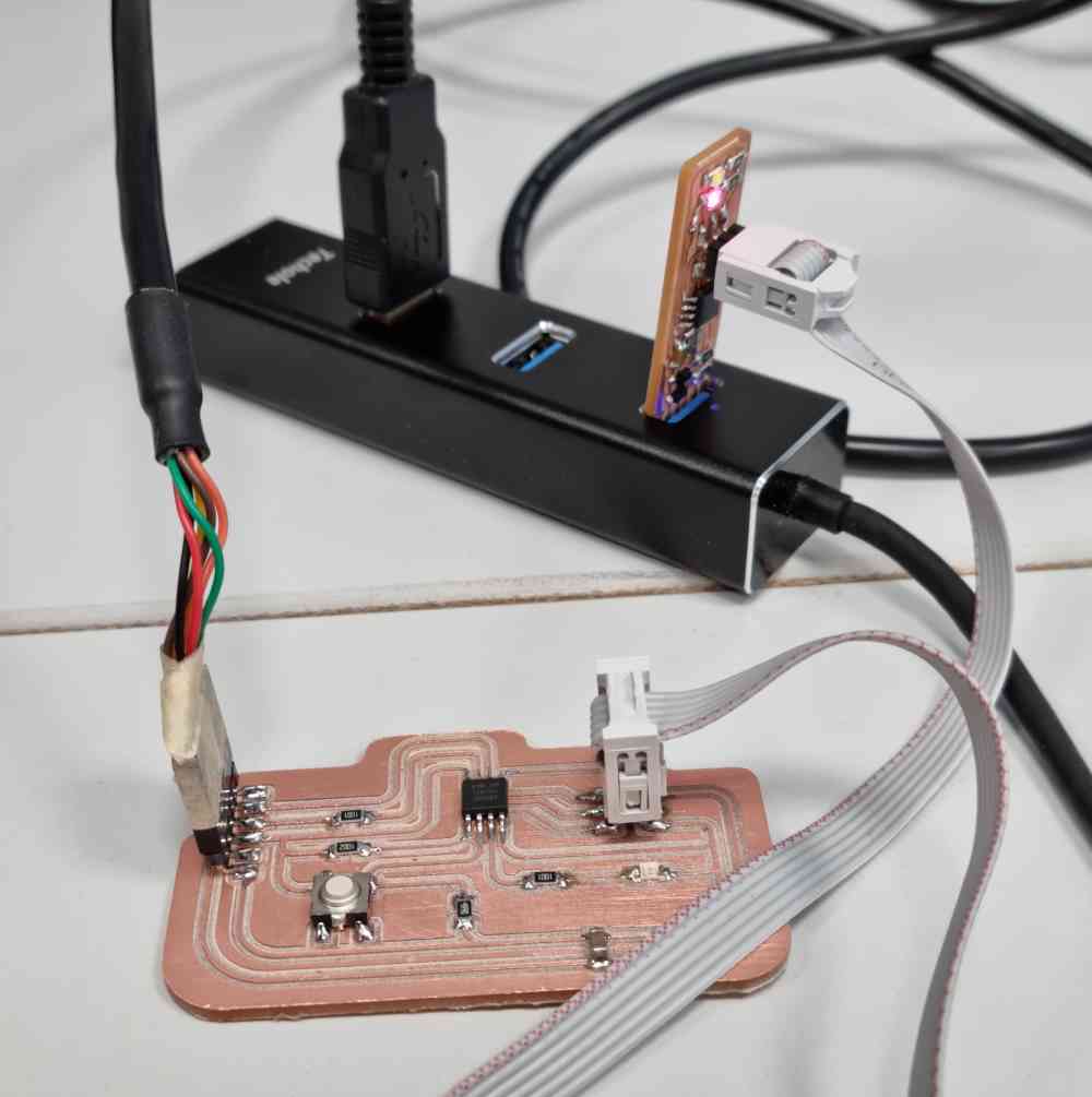 Programming it.
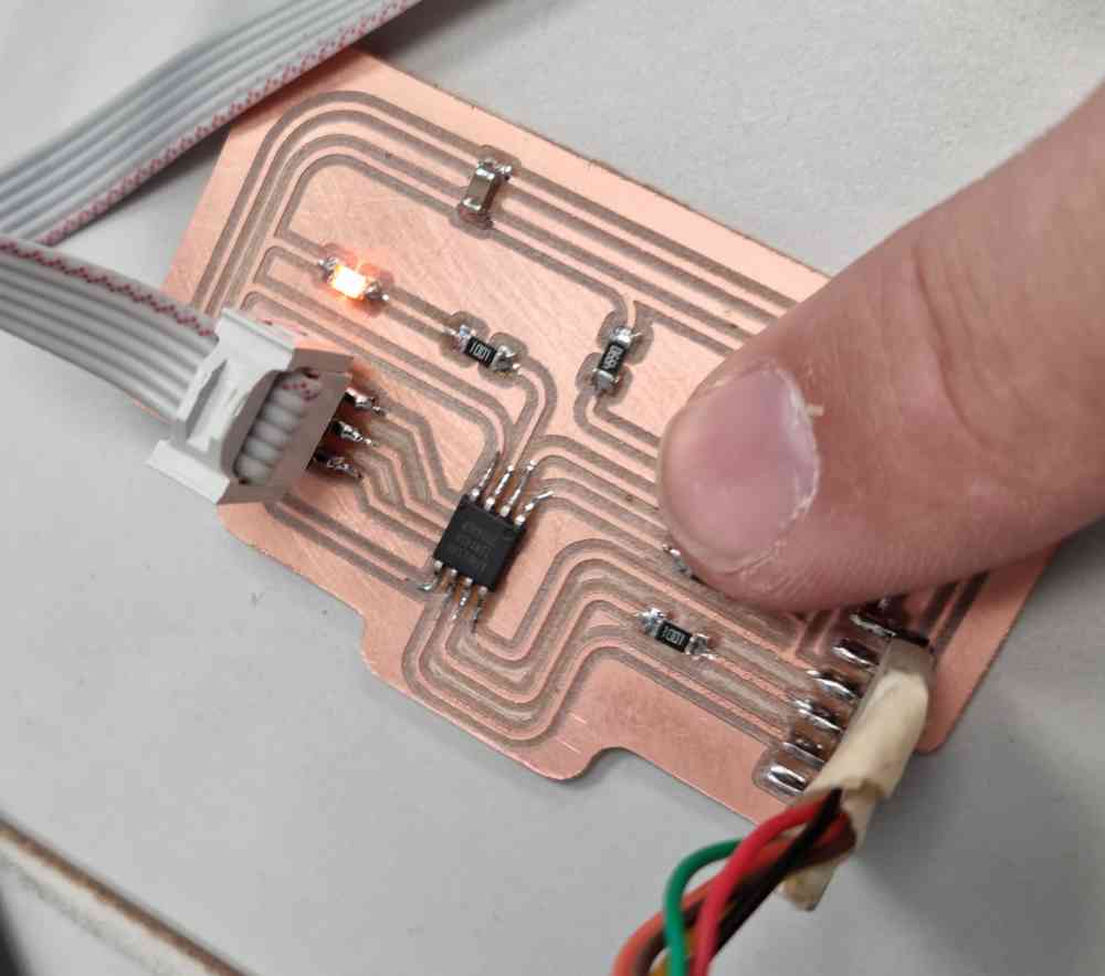 Communicating!
For final thoughts... well.. I really enjoyed this week assignmnet.. I said it on week04 too, I think that weeks like this, with no space for creativity, just follow the instructions benefits me, because of my lack of background. I have to admit that I got stuck with the traces width during the PCB design, but once that was solved, everything else went better than expected. I would lie if I didn´t say I felt really relieved and excited when that little led turned on! If I had to do it again, following the regional review recommendations, I would use different FTDI headers to avoid the risk of tearing it out again, would try out another software such as Kicad, and finally would use another microcontroller like the SAMD11. But, I know i´ll have time for that!
Back to top