WEEK 04: ELECTRONICS PRODUCTION
For this second group assigment, my "fabmates", Esther Pizarro , Jon Merino, and I have to characterize the design rules for our in-house PCB production process. In our FabLab FablabUE Madrid, we are going to use the Modela MDX-40A, so let´s start documenting!
- As we´ve got 0 background or experience in designing, creating and programing a programer, we plan our time management for the grupal assignment as follows:
- Design a PCB.
- Documenting the Modela MDX-40A, and our PCB production process (Grupal assignment).
- For the INDIVIDUAL ASSIGNMENT , we have to make an in-circuit programmer that includes a microcontroller, and test it to verify it works. So, my planning will be:
- Create a PCB.
- Document, learn to solder and solder!
- Program my programmer, test it and make it work!
GROUP ASSIGNMENT
PCB DESIGN
To start with this week´s assignment, after reviewing some past repositories Alberto Gonzálex, Adrián Torres, we had a test hand-on tutorial with our instructor, due to the fact that it seems that the most frequent used program to work with, called fabmodules, doesn´t give online support anymore, we have to use modsproject.org (mods CE) instead with our MDX-40A.
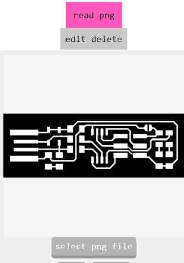
So, our first step is to transform our traces, and board outline .png to .rml files. To achieve this, we plan and decide to build Brian´s FabTinyISP by following, firstly these steps in modsproject.org:
| Open modsproject.org. |
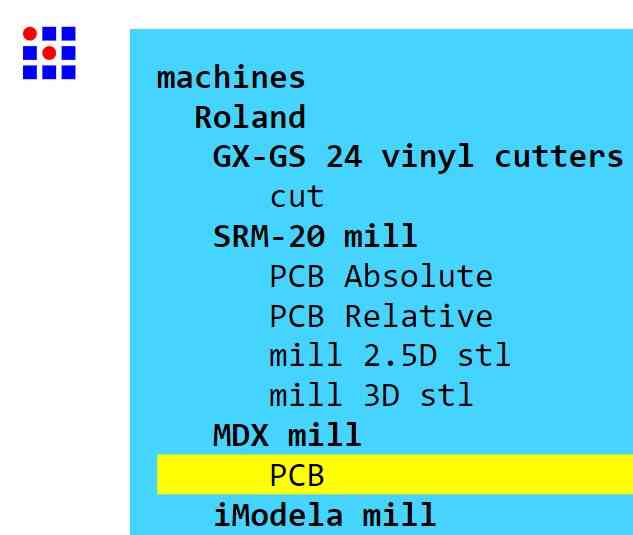
| Open program -> machines -> MDX Mill (PCB). |
| Load your traces .svg or .png file with 1000-dpis. It´s important to do it at first, or your PCB settings changes won´t be recorded. |
| Select in Roland MDX/iModela the MDX-40 Model. Adjust origin as needed. |
| Configure your mill´s traces or outlines, depending on your file: Tool diameter, cut depth, max depth, offset number and speed. |
| Click on the grey button above the chosen setting, so they will be established: You can check in the mill raster 2D values. |
| Create a new module -> modules -> open module -> file save. |
| Click in mill raster 2D -> CALCULATE: A toolpath view of your design will appear. |
| When you click CALCULATE, a download window will appear. Rename you file, that´s going to be saved with a .rml extension. |
| Open file in the Modela MDX-40A VPANEL: We´ll check this further on. |
| We have to do the same with the other file: outlines. |
 MDX Mill
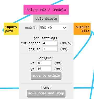 Model select
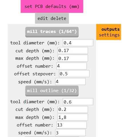 Mill traces settings
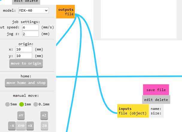 Save file
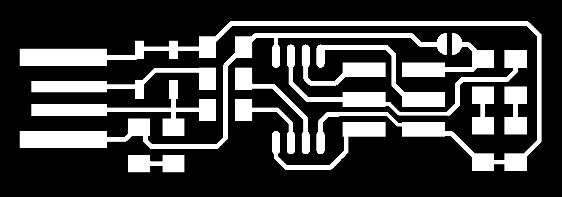
Here below you can see the toolpath view of your design once you click CALCULATE. Blue lines are the milled lines, red lines not, they´re the mill direction/path. These image is very useful because you can check that your cut depth is correct, that will help you avoid breaking milling cutters, specially in the outline file (we learnt this by hard).
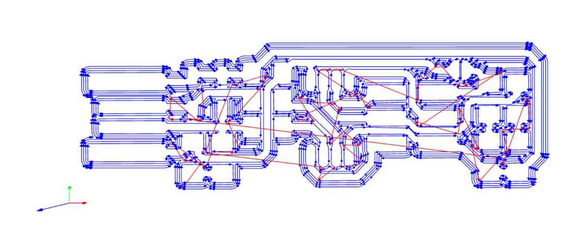 traces tracepath
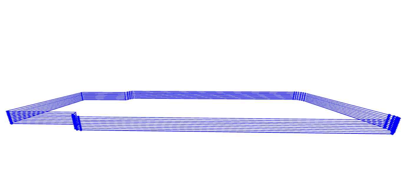 outlines tracepath
Download the .rml files created: Fablab.UE Madrid traces .rml or Fablab.UE Madrid outlines .rml
For first impressions, it was a surprise to test a program not used before by our instructor, once you understand the settings needed to configure, in order to cut later in the Modela MDX-40A, it´s an easy protocol. Probably, the most important part is to know before hand the milling tool diameter that your going to use in every part of the process (traces and outlines) and the PCB clad board to use.
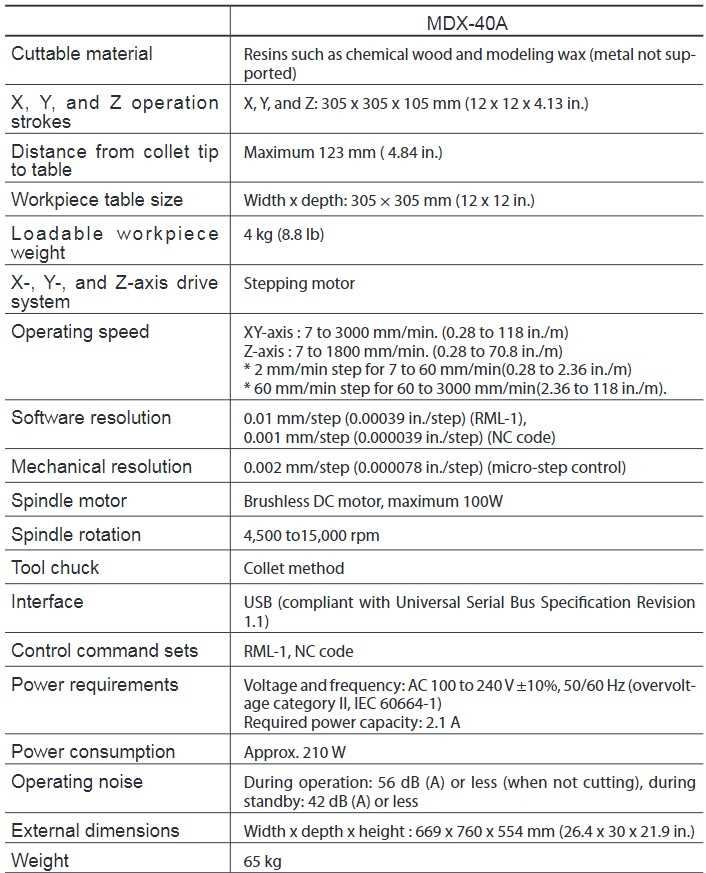
In our case, we are going to use a copper FR1 clad blank board and the setting established for the traces, in our Modela MDX-40A, were:
- Tool diameter: 0.4mm
- Cut depth: 0.17mm
- Max depth: 0.17mm
- Offset number: 4
- Offset stepover: 0.5
- Speed: 4mm/sg
The values configured for the mill outlines, for our Modela MDX-40A, were:

- Tool diameter: 0.6mm
- Cut depth: 0.2mm
- Max depth: 1.8mm
- Offset number: 3
- Offset stepover: 0.5
- Speed: 3mm/sg
MODELA MDX-40A + PCB PRODUCTION PROCESS
Now that we´ve got our .rml files ready, it´s time for the next step on this week´s assignment. First of all, let´s have a look to our Modela MDX-40A:
SAFETY PROCEDURES
This device is designed for laser milling, and it needs to follow some general requirements to ensure that no damage is done:
- Check always that the cover is closed, if not, the machine won´t start the milling process.
- Remember that the end mills are sharp tools, inadverted contact can cause injury.
- Never touch the spindle head after milling, it can be at high temperature.
- Never use a pneumatic blower:cutting waste may get inside the machine and cause fire or electrical shock.
The Modela MDX-40A is a milling machine that can, basically, be dividied in two specific parts:
The workpiece table, or the layer where our copper FR1 clad is going to be set.
The spindle head, were you´ll change the endmills and calibrate the Z axis for the VLS.
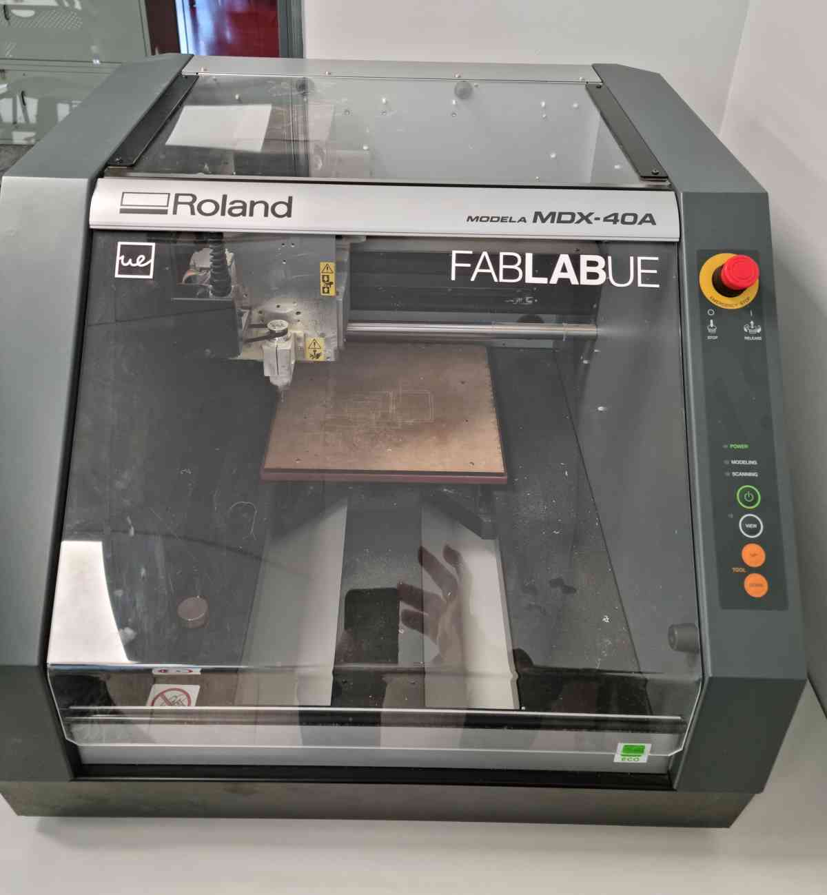 Modela MDX-40A.
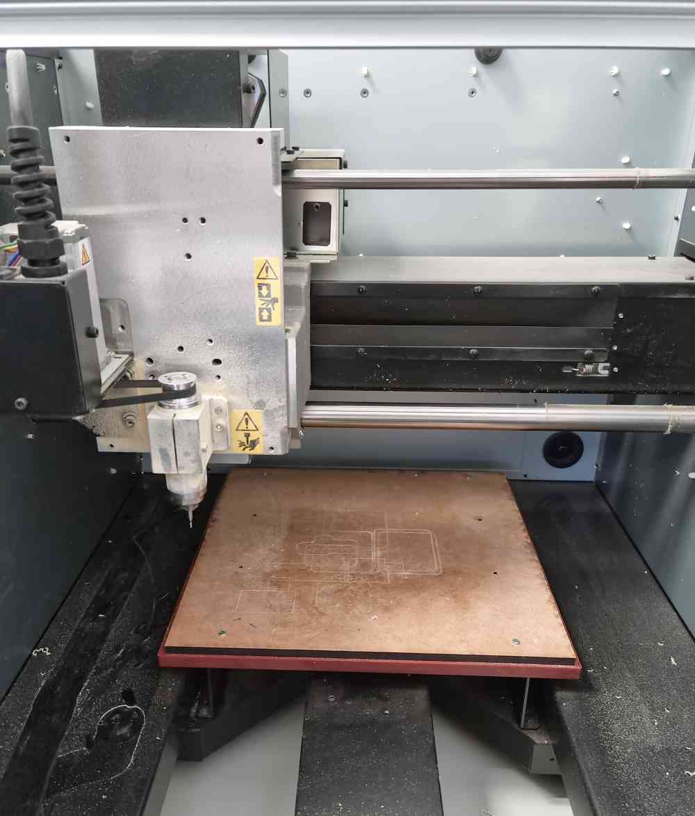 Layer and endmill tool.
PCB PRODUCTION WORKFLOW
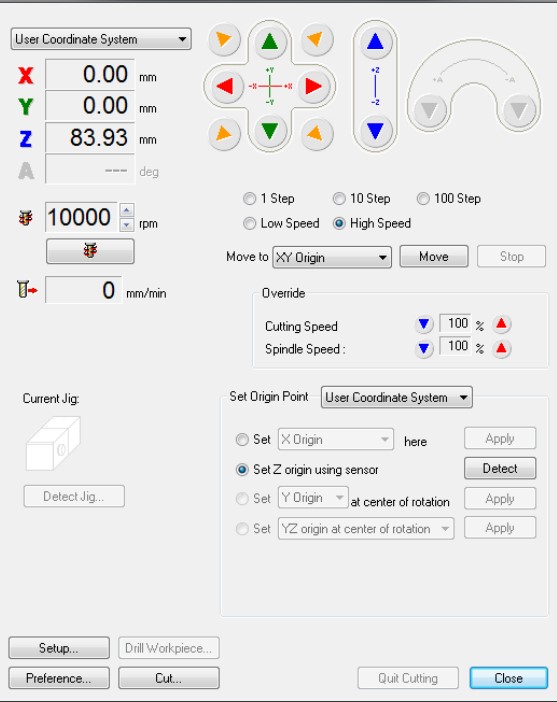
So, to start with the Modela hands on, first of all we open the VPANEL (a dedicated program for controlling the machine) in our windows computer. From this program we´re going to be able to move the table in the Y axis, and the tool in the X and Z axis. And it´s also the program where we´re going to set our (0,0,0) coordenates. So with the help of the VLS program we:
| Open the Modela MDX-40A lid and attach our PCB FR1 clad with masking tape:It´s important to seal it strongly. |
| Change the tool for milling: It´s important to protect the tool from falling and breaking. Grab firmly and lower gently. To tightening, snug gently. |
| To change the tool: Use the two wrenches, don´t touch the tip of the tool (it can break!), close without putting too much strenght. |
| When changing tools, the big wrench on the left and the right wrench on the right, close them together to loosen up. Put the wrenches on the other hands and you will tighten the tool. |
| Go to the VLS: Set X,Y origins with the VLS control pad, and once set, go to XY-> APPLY. |
| To set Z origin: Use the Modela Sensor (Set on top of the PCB FR1) and detect. Don´t forget to remove the sensor and the cable after. |
| Check the RPM´s: In our case, we settled them at 15.000RPM´s |
| Press CUT in the VLS: Select the .rml file to cut. |
| Press OUTPUT to start cutting. DON´T FORGET TO CLOSE THE LID! |
| Once the cutting has finished, it´s important to vacuum to remove the cutting waste. |
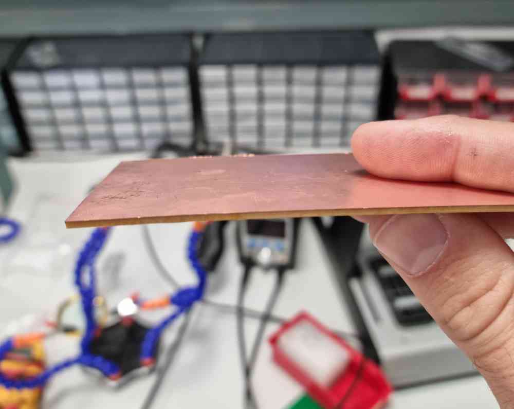
| Clean and sand the piece. |
| Start again with the outline file: Don´t forget to change the tool, and set Z to it´s new origin. |
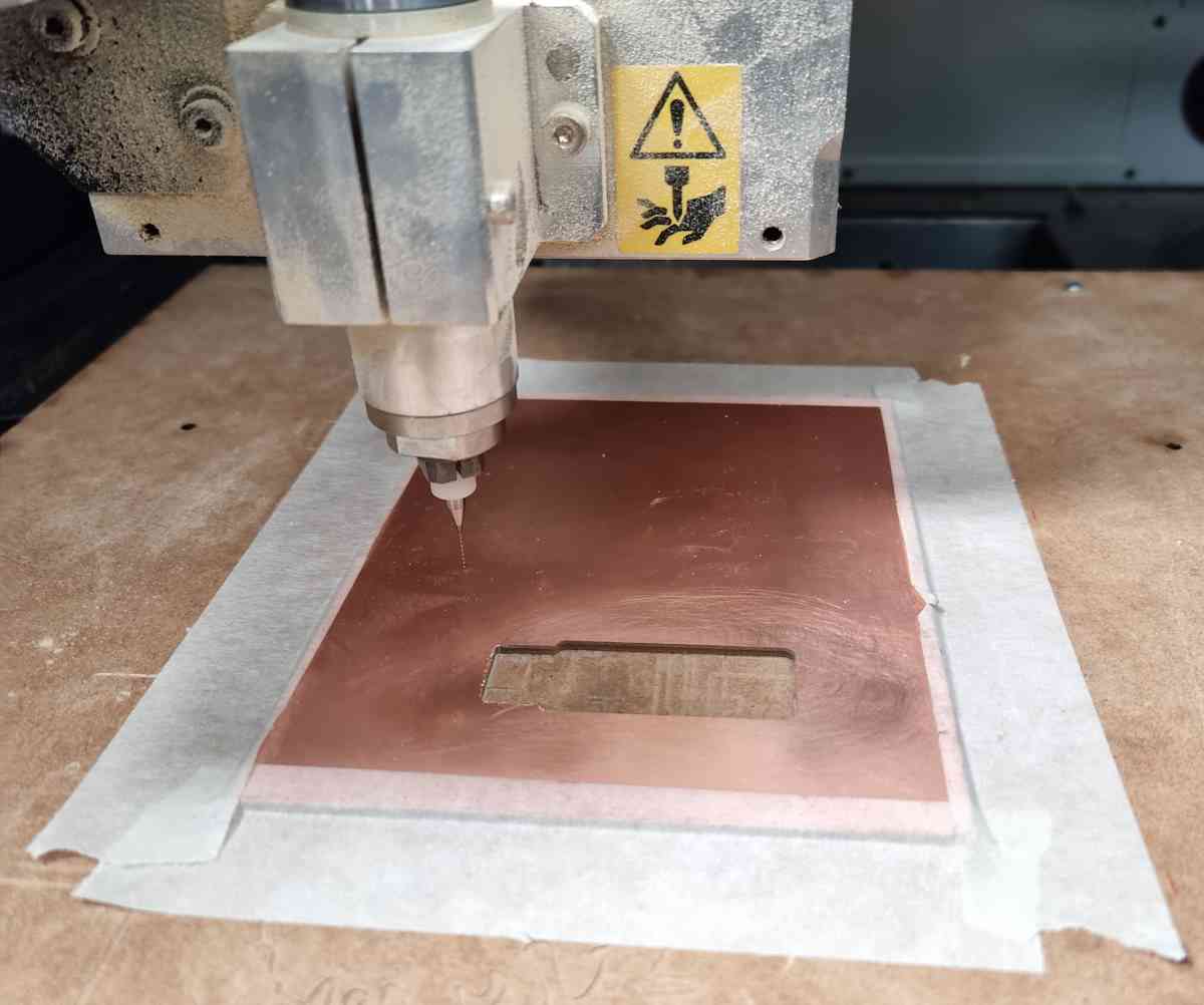 FR1 PCB attached.
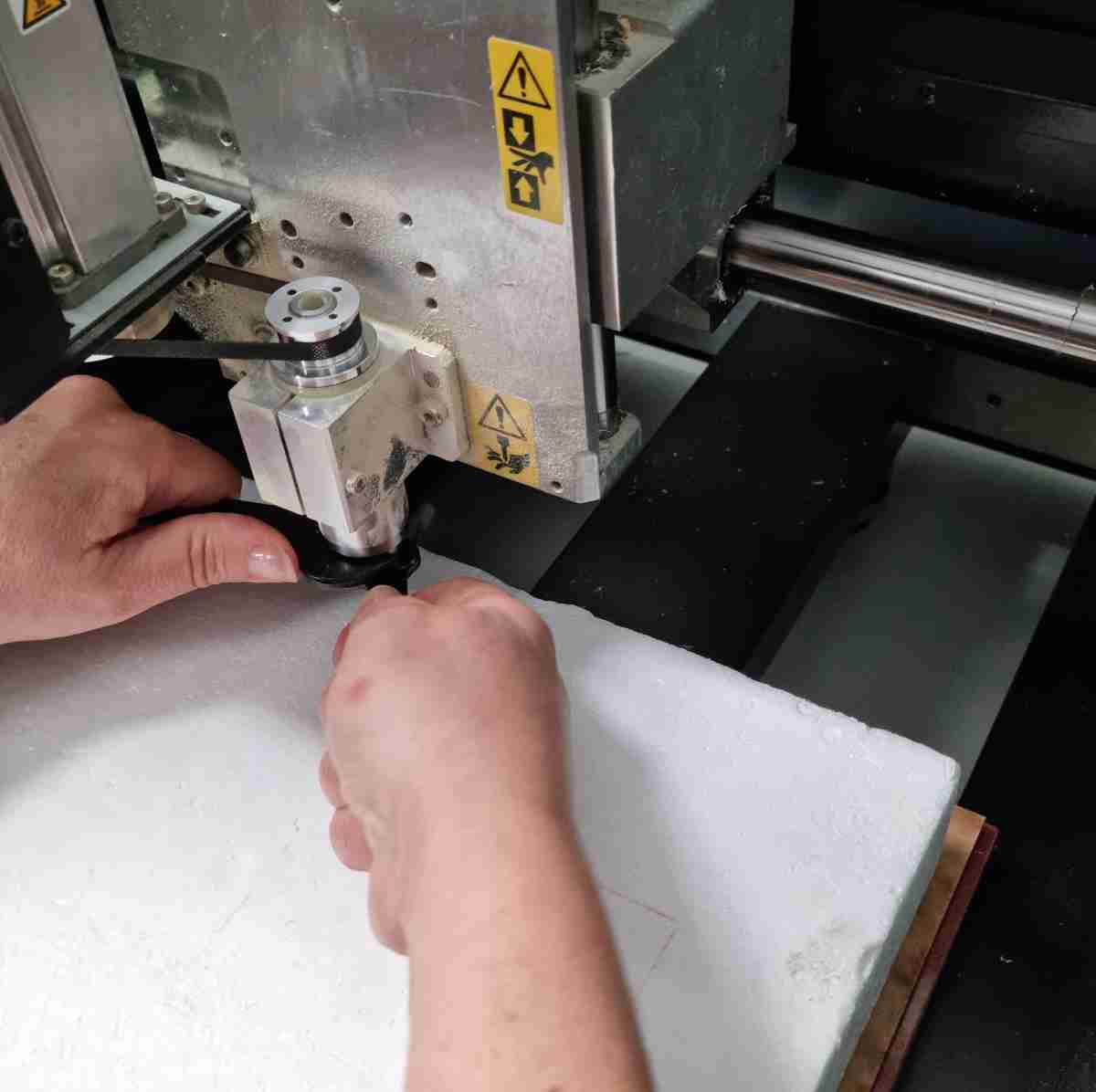 Tool protection cork.
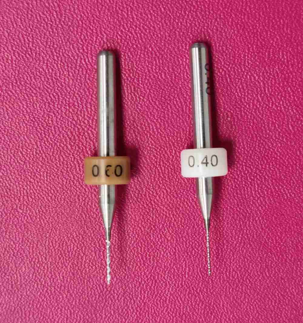 tools.
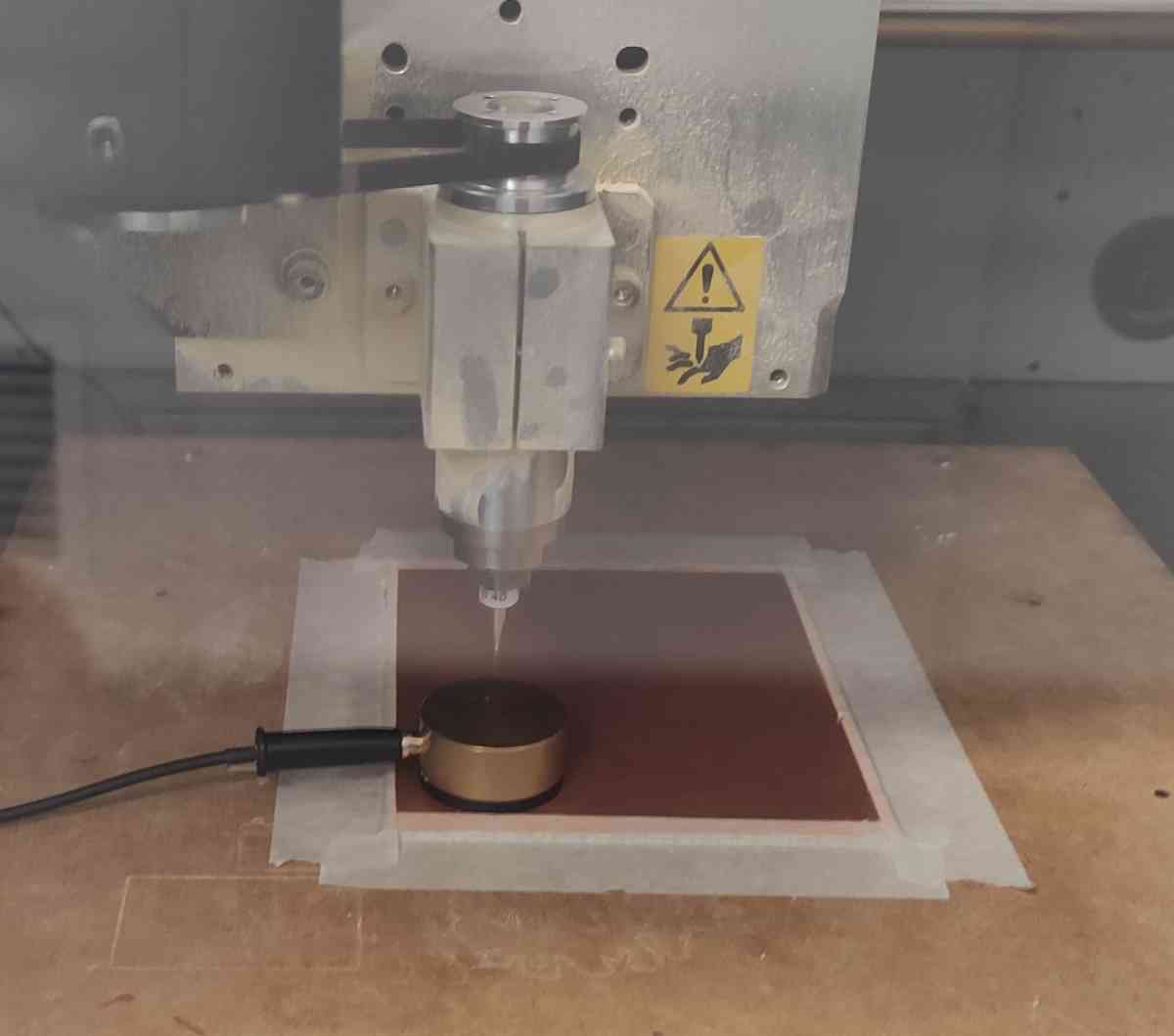 Sensor.
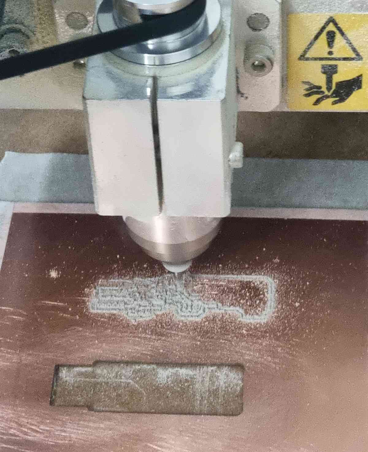 Cutting.
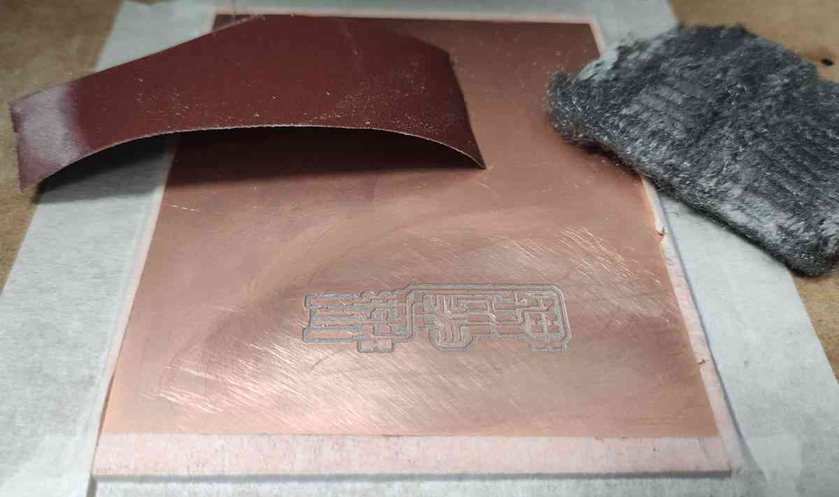 Sanding.
For thoughts and impressions, it gave us (the three of us!) a big headache and took us some precious time to start milling properly. The issues we encountered were that the first PCB FR1 board that we used was combed, but we didn´t notice until the firts mills. Secondly, we didn´t realize that the X,Y settings on mods CE are preestablished in 10mm, and that took us some time to figure it out aswell. In this case, you need to re-do your .rml file with the desired X,Y settings. We also had some issues with the tools, we broke our first one because we didn´t check on the toolpath view (mods CE previously explained above) the cut depth for the outlines, so we gave it too much depth at first (you can check it on the video below). The second tip we broke was a mistery because we double checked everything but it still broke at the first touch with the board during the milling, but it worked well at the second attempt. But once everything was sorted out, the milling wen´t fine since then.. and hopefully will stay this way..!
As for the personal thoughts, I really like this machine, it´s amazing the precision with which it cuts, and it´s quite fast too. So, for sure, i´ll keep on using it as much as I can during the fabacademy.
 PCB FR1 before
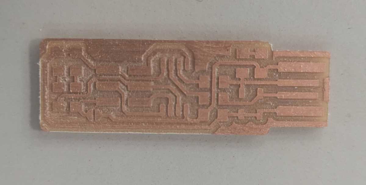 PCB FR1 after
INDIVIDUAL ASSIGNMENT
SOLDERING
Now that we´ve got our board ready, it´s time to solder. So the components nedeed to fabricate a FabISP are:
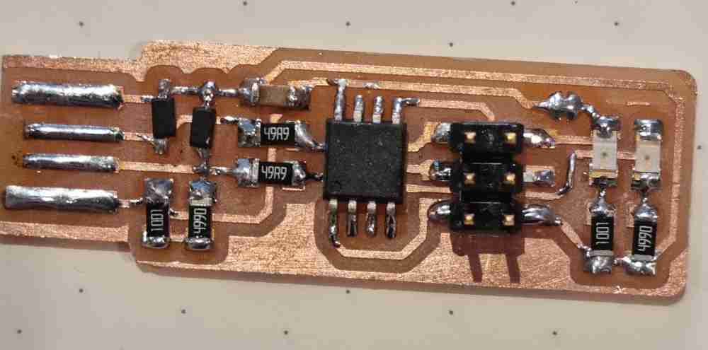
- 1x ATtiny45.
- 2x 1kΩ resistors.
- 2x 499Ω resistors.
- 2x 49Ω resistors.
- 2x 3.3v zener diodes.
- 1x red LED.
- 1x green LED.
- 2x 49Ω resistors.
- 1x 2x3 pin header.
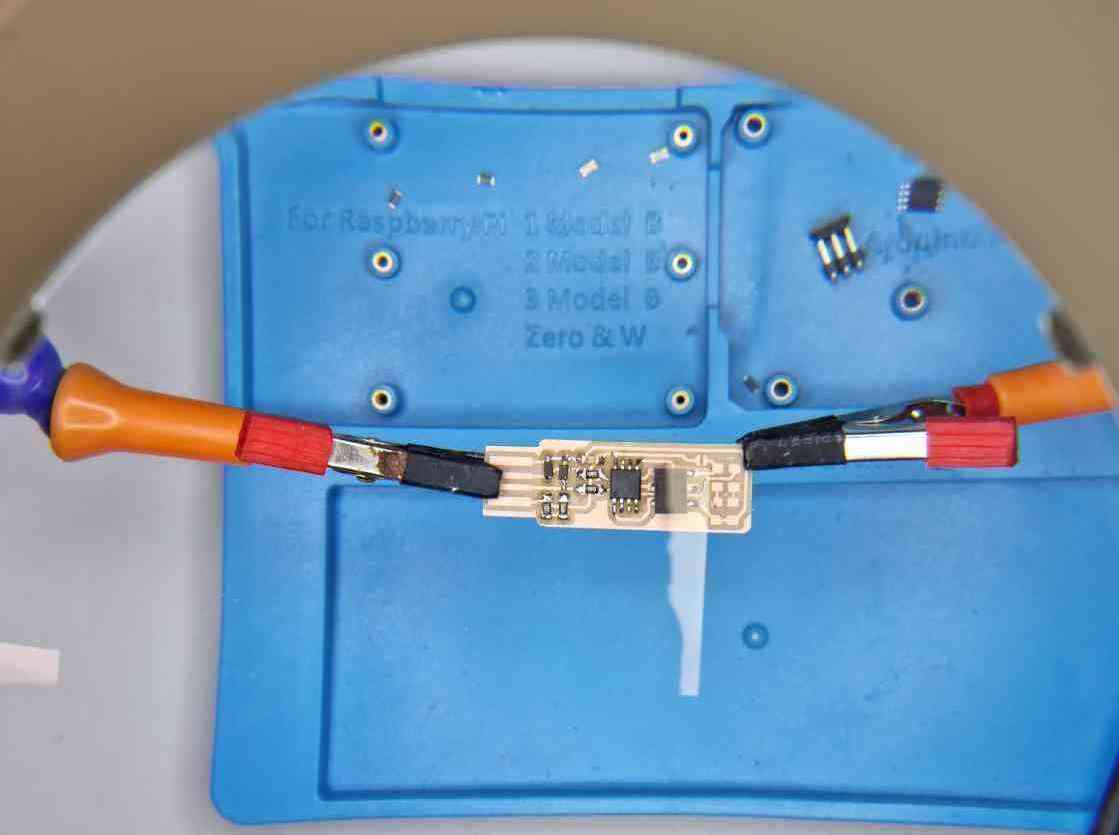
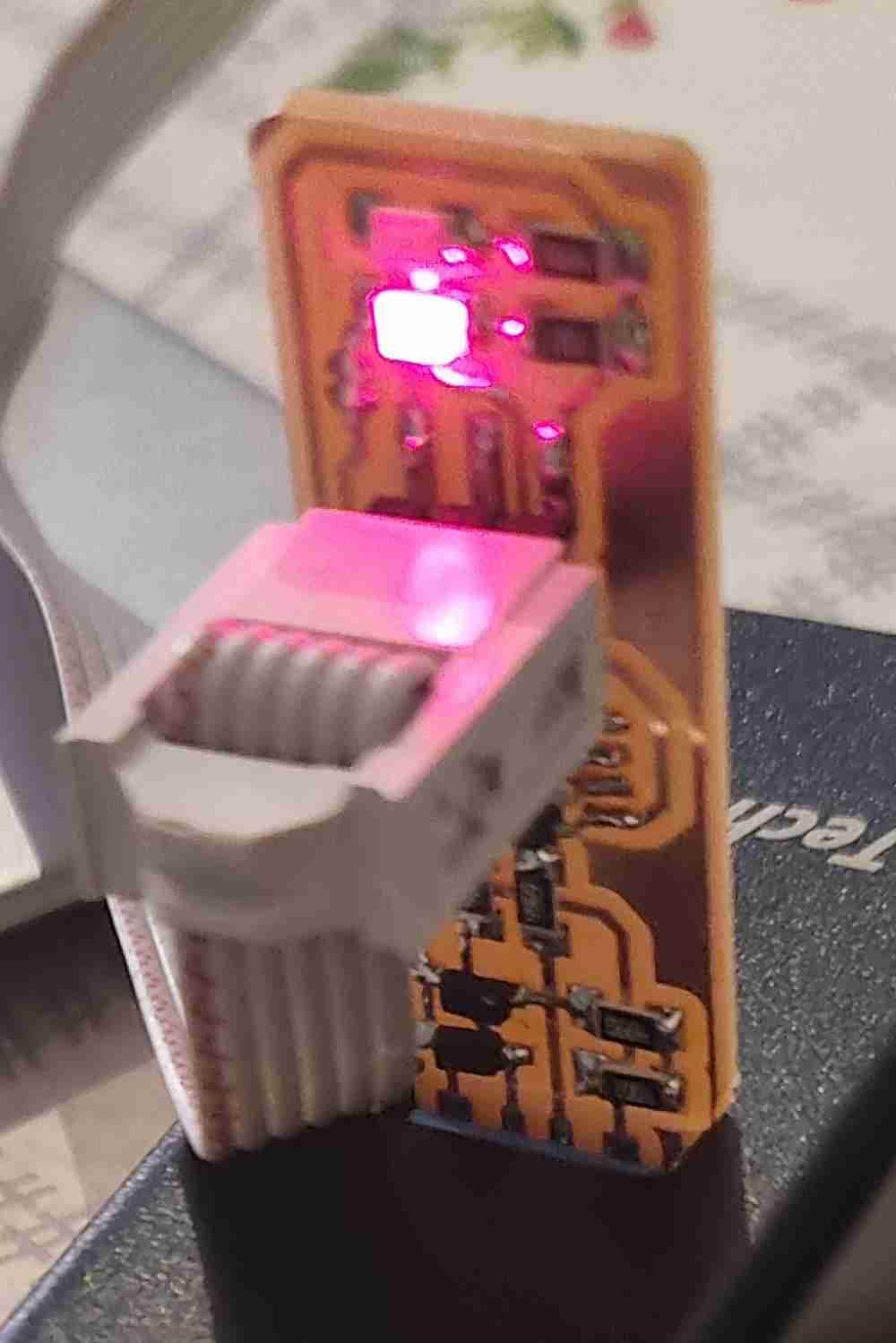
- Here on the left is my board after soldering.
As i´ve never solder before, didn´t even get close to a soldering iron.. to attempt with guarantees my first soldering, I followed these steps:
| Prepare your work area with all the components neatly placed so you can easily acces them. It helps to have a screen close were you can check the diagram of the board you are soldering. In our case, a the schematic image from Brian´s FabISP tutoral (the red and black image on the left). |
| Use a good pair of tweezers and a desktop solder magnifying lamp. Both will make your life much easier. |
| First clean your board and cut the copper at the tip. |
| Check that your iron tip is clean, and wait until it´s heated enough.In my case it was set to 340º Celsius. |
| To start assembling a component, add some solder on the copper pad first. Then, add the component, iron the solder and wait until it flows, and remove the iron gently. Good joints should look shiny and smooth. |
| Now that the component is fixed, the other parts of the same components will be easier to solder. |
| Rembember that some components need ORIENTATION. |
| It´s better to start soldering the smallest in the center first, and then the bigger from bottom to top. |
| If we make mistakes, we can de-soldering. |
| Once finished, remember to clean up. And to turn off the iron! |
In order to finish the process, don´t forget to lime the copper that´s on the tip of the USB shaped board
 Components to sold.
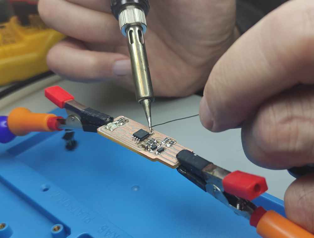 Soldering process.
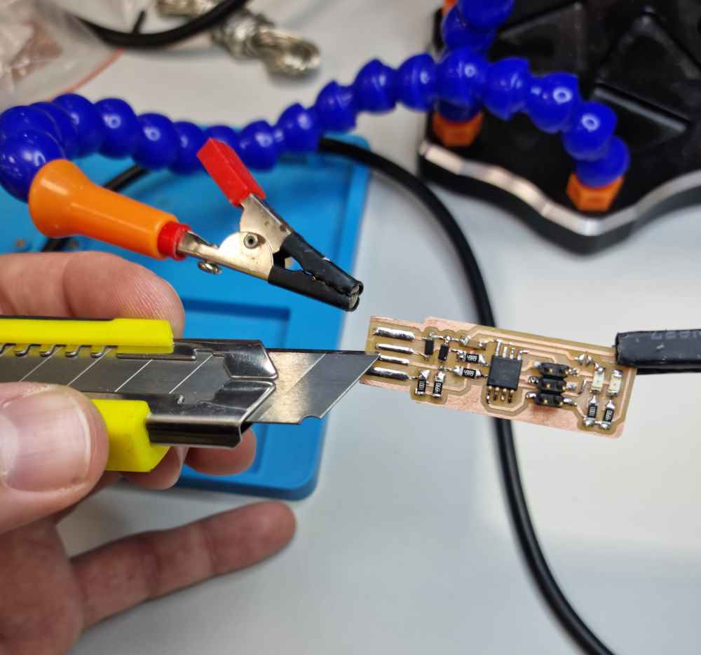 Removing the copper from the tip.
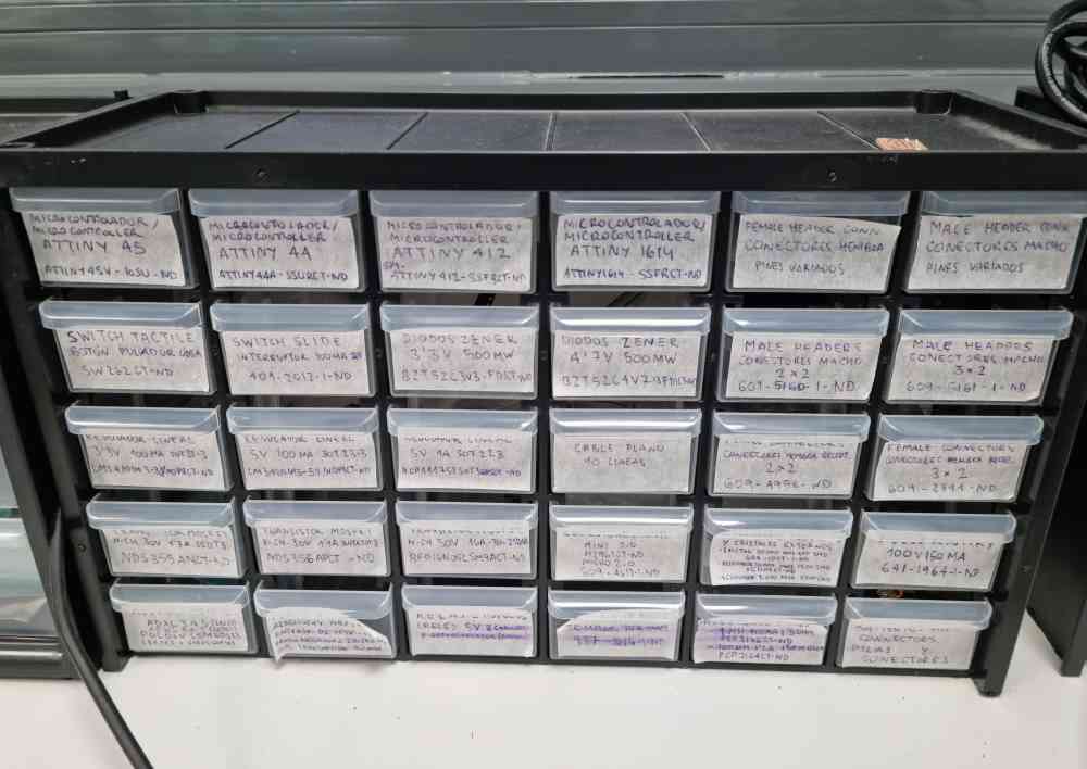
As you can see in the images above, we have all the components stored and labeled to facilitate its location. And, at the bottom of the label, they have the Digi Key serial number to provide the needed information when requesting resuply.
For final thoughts, I can´t beleive that with only a quick first practice before stuffing my components, i´ve managed to solder properly a functional board at the first attempt! (I now it´s functional because I managed to progam it correctly with no soldering issues). Really happy for what i´ve achieved, not bad for a newbie! To be honest, I had checked a couple of tutorials that helped me to understand the process and gave me confidence on the steps I had to take, such as SDM soldering tutorial.
PCB PROGRAMMING
As we are going to progam an ATtiny 45, we folloed Brian´s mandaroty tutorial, in combination with Sergio Herranz´s to avoid problems with the Atmel AVR toolchain for windows installation and setting.
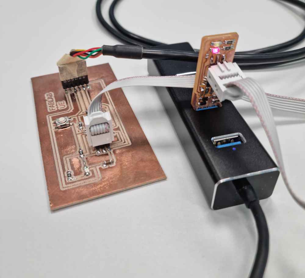
First of all, It´s important to understand how are the FabISP (mother programmer) and our recently created FabISP connected to our windows pc. In this case, the FabISP mother programmer has to be connected to our laptop, and through the 6 pin bus flat cable we connect it to our FabISP, which will be connected to an external power supply (not to our laptop) also. Once that we got that sorted out, I downloaded the following programs:
- avr8-gnu-toolchain-win32_x86-master:In this case, I need to give credits to my fabmate Jon Merino, because he shared with me this lifesaving link: Carlos siles-avr8-gnu-toolchain-win32_x86, were you can download it following the readme instructions. A very useful link, because it´s tricky to find this program.
- GNU Make: In this case just follow Brian´s mandatory step by step GNU AVR Chaintool instalation for windows.
- avrdude: We follow again Brian´s tutorial just mentioned above.
- Zadig:You can also find the link on Brian´s tutorial.
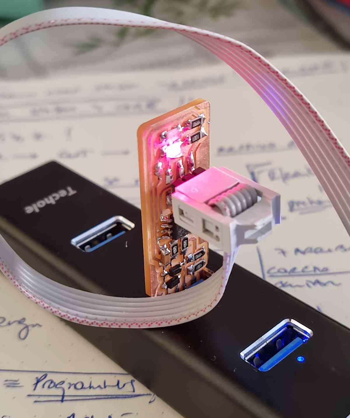
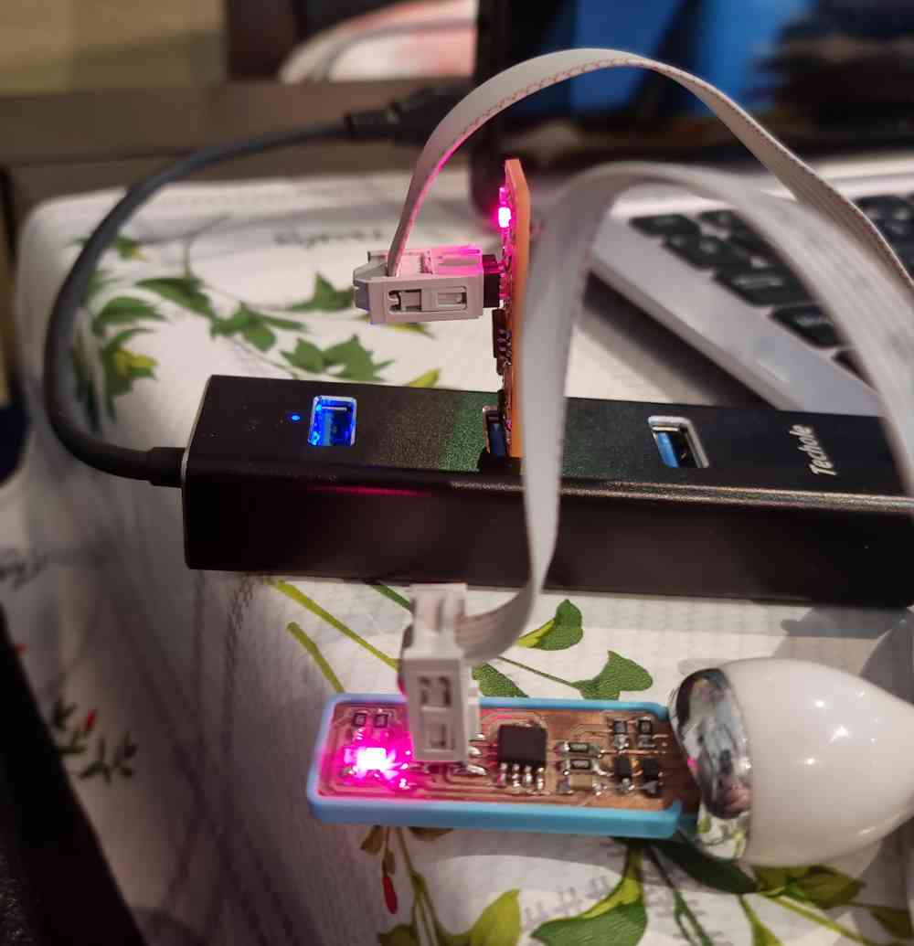 Mother FabISP connected to our laptop.
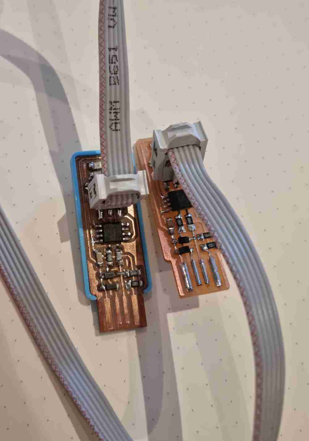 6 pin bus flat cable connecting both FabISP.
Now, once we´ve installed the programs, and before running Zadig, we need to update our PATH on your systems properties (you guessed it right, just follow Brian´s tutorial). But be careful to set your own laptops paths for the three new added programs! Now that our programs are installed, we need to check that our mother FabISP and our own FabISP are correctly connected with the 6 pin bus flat cable and correctly usb powered. If we did everything allright up to here, we just need to open Zadig, select the USBtinyISP (programmer) and install libusb-win32(v1.2.6.0).
It looks like the drivers were succesfully installed (Olé!), and to ensure that every that we installed works, we run a SANITY CHECK, and it looks like all the commands we installed work!
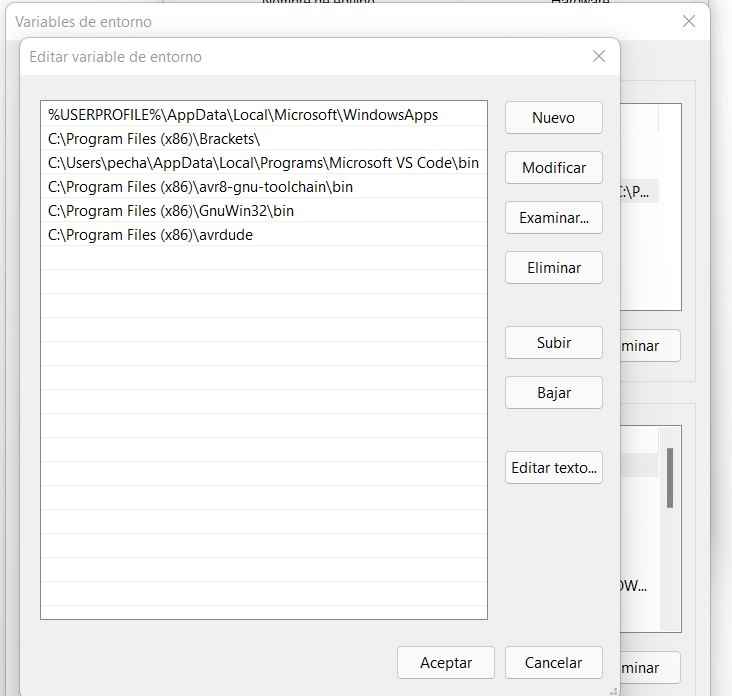 Update PATH
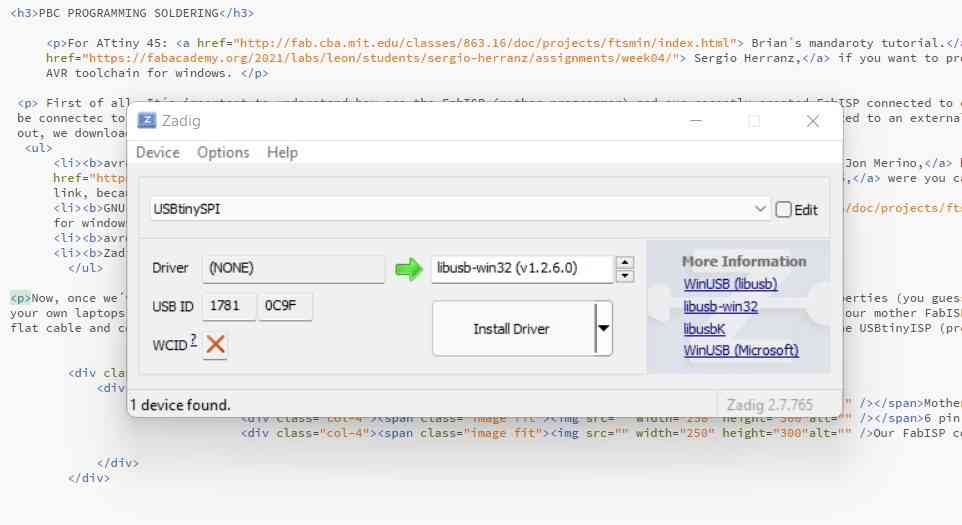 Drivers installation.
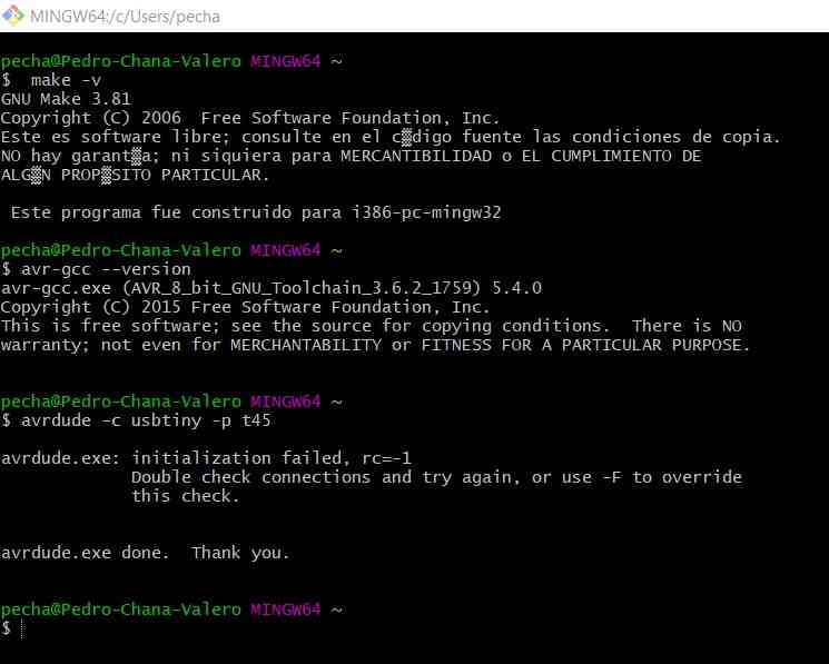 Sanity Check.
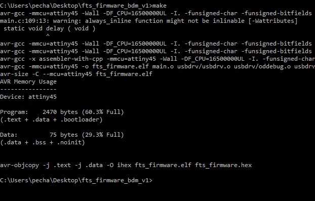 Firmware source code.
For the final steps, we need to download and run our last firmware source code. In this case, we just followed Brian´s tutorial steps. And as you can see in the image above, you will have a filed called fts_firmware_hex if the command completes correctly. Now we´re read to program our FabISP.
ATtiny45 PROGRAMMING
For this final step, we follow the simple instructions of Adrián Torres repository, because I find Brian´s instructions a little confusing regarding were to connect the "mother board" and were to connect the board we want to program (our board). So, the final steps made were:
| Connect the FabISP "programmer" to our computer via USB. |
| Connect FabISP "programmer" with our FAbISP with the 6 pin bus flat cable: Be careful and be sure that the cable is correctly connected with the ISP header. Check that the red line of the cable is at the left side of both FabISP. |
| Check that our led red light is on. It´s important to check that the solder jumper is bridged. |
| Run Make flash command on Git Bash. Check that your in the same directory were you created your fts_firmware.hex |
| Run the Make fuses command on Git Bash. After, unplug both boards and plug ONLY our board to check that the USB on our board works. |
| Open Windows lists USB devices in Device Manager and check that your USB is detected. |
| If up to here everything work properly, connect boards as before and blow the RESET fuse by running on Git Bash: make rstdisbl. |
| REMOVE the bridge on the solder jumper. In order to disconnect Vcc from the Vprog pin on the ISP header. |
| And you´re done! Enjoy your first FabISP. |
 red light in our FabISP.
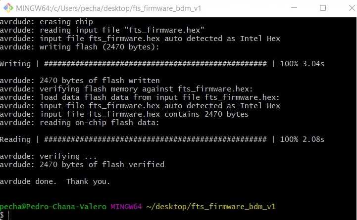 Make command on Git.
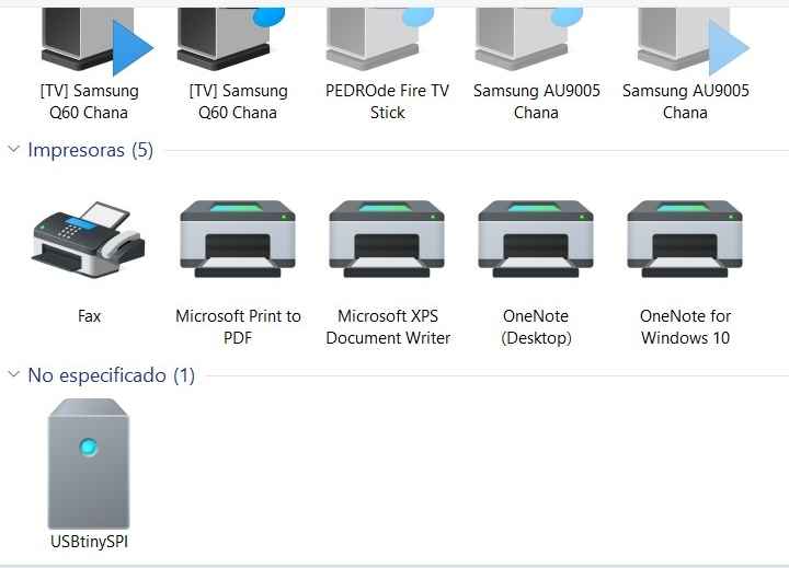 USB detection.
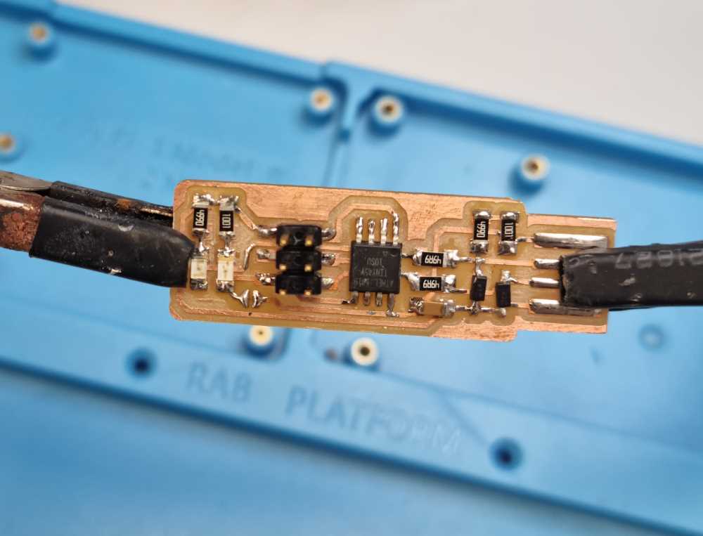 Removing the bridge.
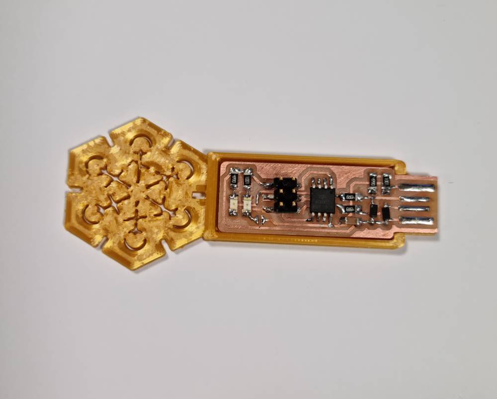 FabISP programmer ready to use.
Now that we´ve got a functional FabISP, thank´s Jon Merino. for the personalized usb cover!, it´s time to test it, so I borrow from our instructor a programable board, and with the help of arduino IDE I uploaded the code sucessfully!
 Connecting it to another board.
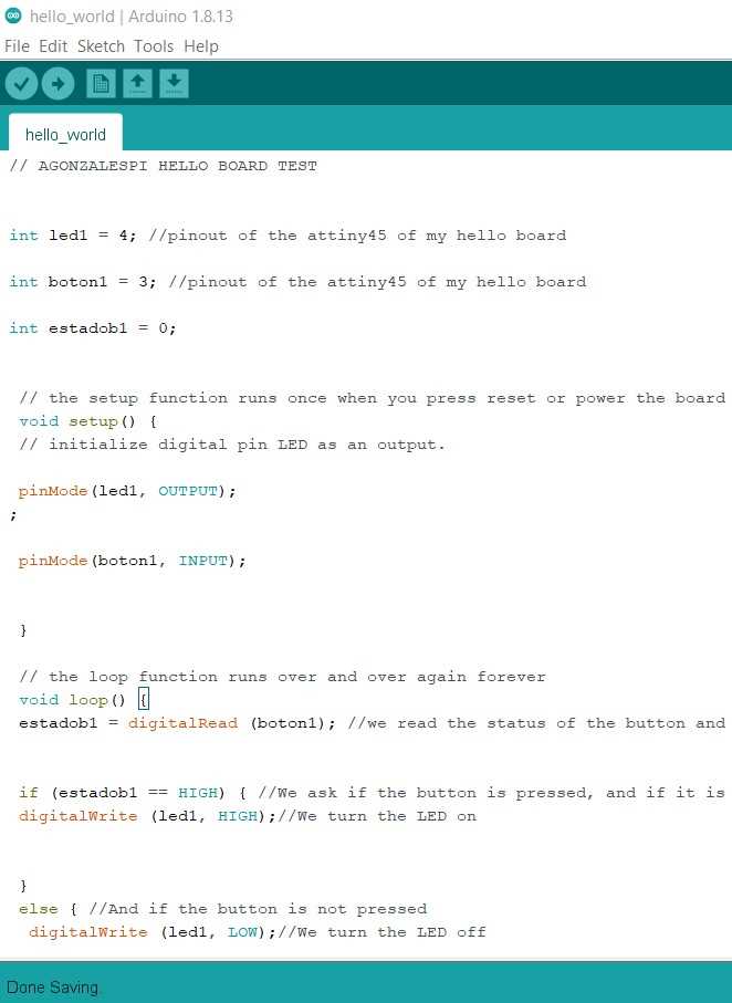 Using it as a programmer.
As for my experience, as expected, it didn´t work at the first try. I didn´t run Git Bash on the same directory were I had created the fts_firmware.hex. But, after solving that little issue... I had no problems running "make flash" and "make fuses" command. My pc detected my board and finally didn´t have any issues with the "make rstdisbl" command, remember to run it on the same directory as the one you used before, and just take the bridge on the solder jumper, and now you can show off with your brand new, functional FabISP..!
This final part has many steps, and you have to install a lot of commands, but if you take time to do it without a hurry, and follow step by step you shoudn´t have much trouble. It took less time than expected, because I really was expecting lots of problems with the board, so happy until now!
For a final reflection on the week, I think that it was a benefit for me to have a very step by step, protocolized week, because I think that my lack of background on this subject was less relevant, at the end, there´s no space for much creativity, just doing!
