7. Electronics design
Redesign Hello-World board
Part of learning to design electronics is getting familiar with tools that are used by redesigning one of the hello world boards. I’m new to using them myself. KiCAD vs Eagle are the software used to redesine hello world.KiCAD was already installed the interface is quite intuitive and easy to learn.
Redraw an echo hello-world board, add(at least)a button and LED (with current-limiting resistor)check the design rules, make it, and test that it can communicate extra credit: simulate its operation
I downloaded Kicad software using linklink After i went to the kicad website and downloaded the worldwide OSDN version for window 10. i watched more tutorals on youtube to get more familiar
Designing process
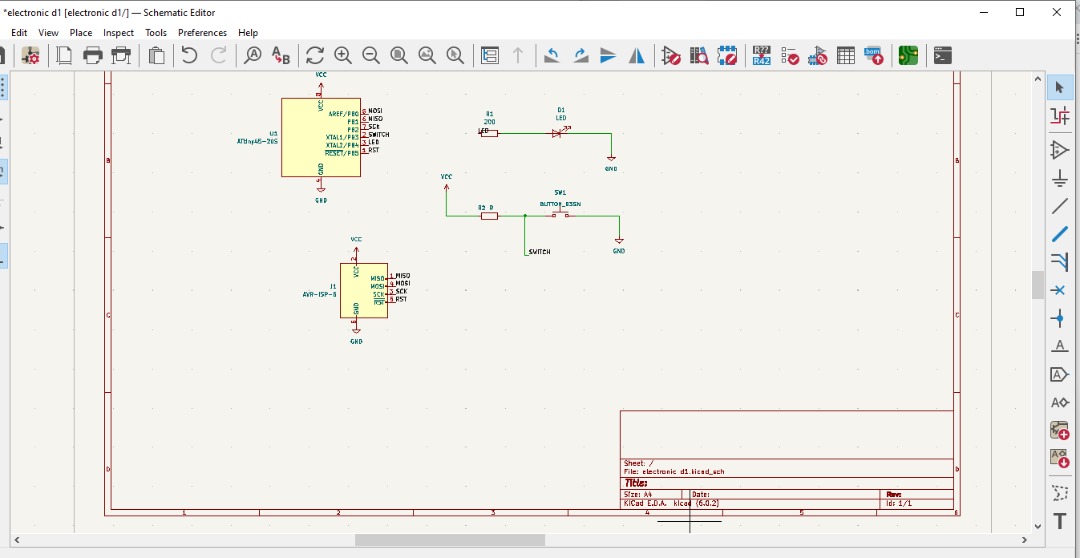
my work was to create a board with a button that act as switch in put.the plan was for the LED to stay on unless the button was pushed. The componts i would use from the previous board would be: .ATtiny45-20s
.Resistor
.LED
.AVR-ISP-6
.Switch (Button B3SN)
.VCC
.GND
Kicad schematic Editor
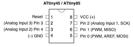
ATTINY 45 DESCRIPTION
ST: Reinitiate communication
PB: Programable ports
GND: Ground.
VCC: Voltage Common Collector.
Data Sheet.
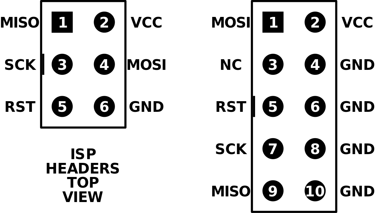
ISP DESCRIPTION
MISO: Master In Slave Out
MOSI: Master Out Slave In
SCK: Clock. Is constant, to set the pace
RST: Reset.
GND: Ground.
VCC: Voltage Common Collector
design rules
PCB design and manufacturing is a complex process managing thousands of components and connections across a multi-layer board. It is of critical importance to ensure the production yield is error-free and one way to improve fabrication yields is to perform
Design rule check (DRC)
Catching an error in the design phase will prevent a product from being scrapped due to power ground shorts, misaligned vias, and missing pins. DRC for manufacturing is important in ensuring the quality of PCBs fabricated on the production line.
What is design rule check (DRC) in PCB design?
A design rule check is a set of rules used by a designer to ensure the schematic matches all manufacturing considerations and dimensional tolerances set for a board. Production processes have a margin of error for the variation in the products that are manufactured. Such variations in production yield are adjusted in the design phase itself.
To learn more about schematic symbols and schematic diagrams, read article
The Meaning of a Schematic Diagram
What is DRC and LVS check?
A DRC allows one to verify the schematic and layout with regard to the margin of error you can incorporate in your design. As it allows one to check if a specific board layout correlates with the original circuit diagram or schematic of the design, it is also called layout versus schematic (LVS) check.
What are DRC errors?
Electronic design automation software lets you know when a design margin is violated by stating the parameter that is out of the acceptable range. This is called a DRC error and it helps eliminate rework in the production stage.
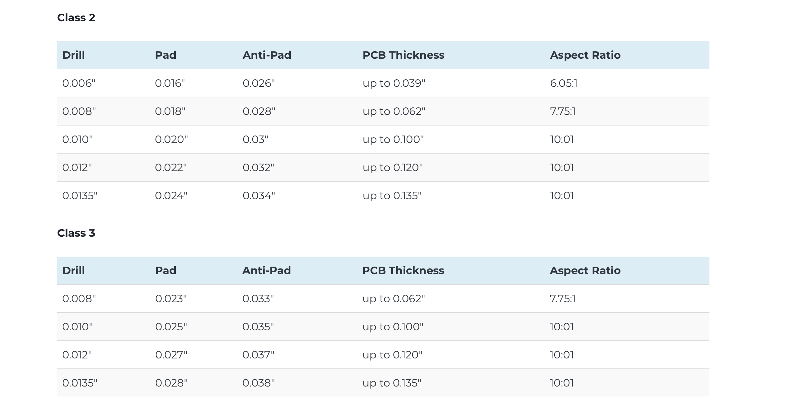
DFM rules
DFM stands for design for manufacturing, which is the layout topology in a way that avoids all the problems that could be encountered during the PCB fabrication and assembly processes.
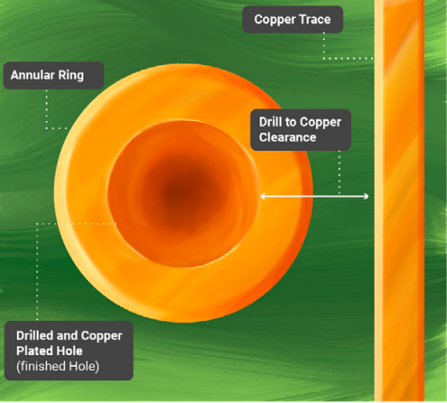
Drilling checks for drilling holes:
- Drill-to-copper: The drill-to-copper is the land clearance between the edge of a drilled hole to the nearest copper feature. The nearest copper feature can be a copper trace, copper pour, or any other active copper region.
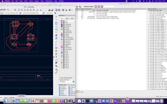
I first had to download the component librarr for FabAcademy first. I used GitLab linkto download the library.i extracted the files and loaded it into a separate directory to incorporate it into Kicad.I added the following,most of the components are from Fab library.
Install Kicad and libraries
For individual assignement I started by downloading Kicad to do the PCB design. After that I downloaded the Fab electronics component library for KiCad.
After a couple of failed attempts I managed to successfully install all the libraries. Then I put all the components I had to make my board into Kicad’s schematic editor.
Because the ATtiny45 board is very simple I used the schematic method using lines between the connections. Advantage is that it gives you a better understanding of the way the circuit works and of the coherence of the board.
PCB design workflow
Designing PCB I started designing the schematic of the circuit.it was my first time to work with KiCAD but it is very easy to use it.
We had instructions which components to use and had to redesign the board with the right connections and values. One way of drawing schematics is the “global label” method where you connect components by addressing them with a label.
When placing components there are a lot of types and footprints to choose from, but there is a specific library called “fab” that displays the components of the fabacademy invetory.Component Values .The resistor in series with the LED is to make sure that the current through the LED is set to the right value.
First steps in Kicad
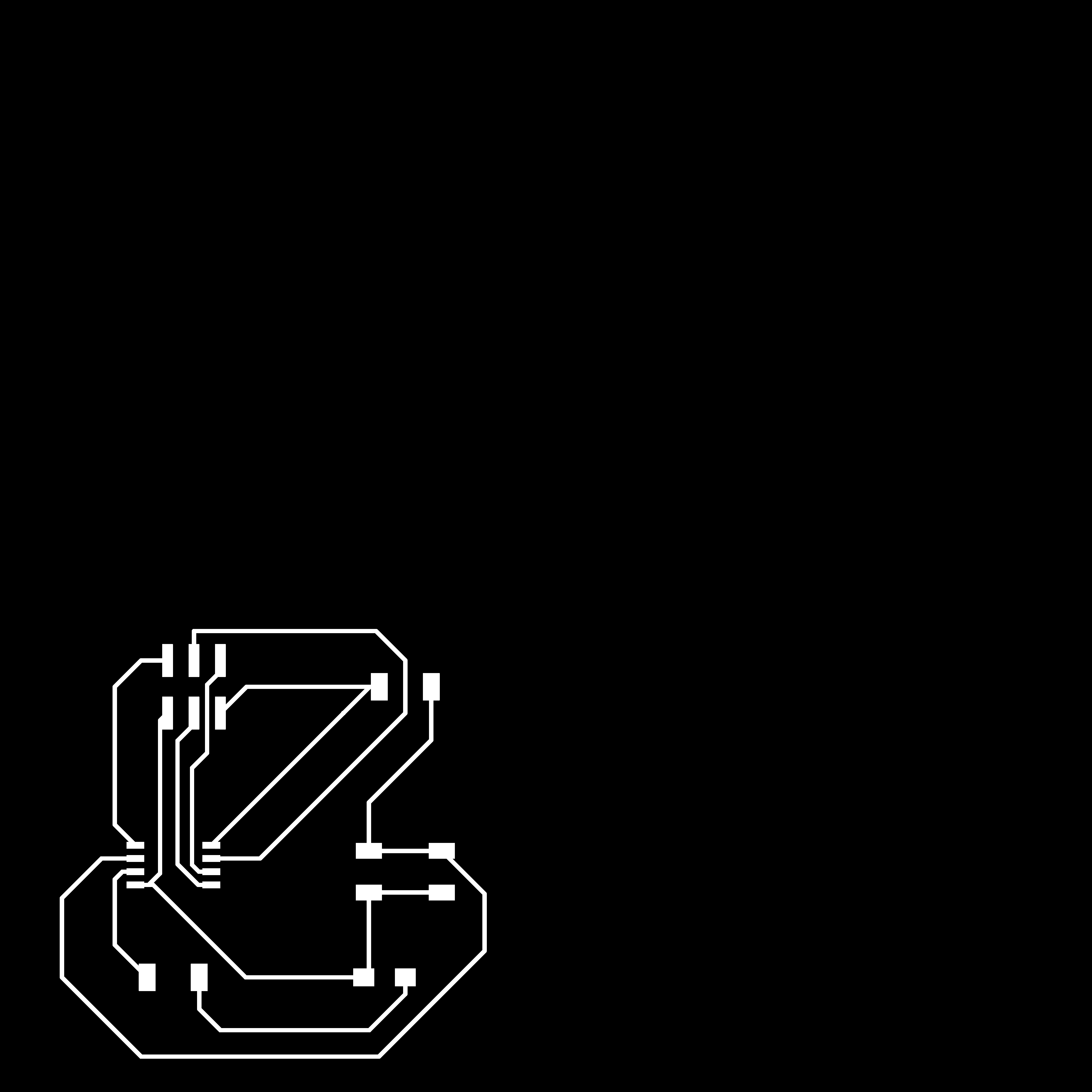
Then I went to the board editor to see where I could pass the paths of each of the components, after trying 20 times and not succeeding, I copied the paths from this link.
Routing
The routing is done manually in the PCB editor. First all components are generated on the board and thin lines represent the connections the way they were made in the schematics. The easiest way I found doing this is to start with Ground, followed by Vcc conections and the rest at the end.Some board setup is needed to comply to the restrictions of our PCB milling machine.
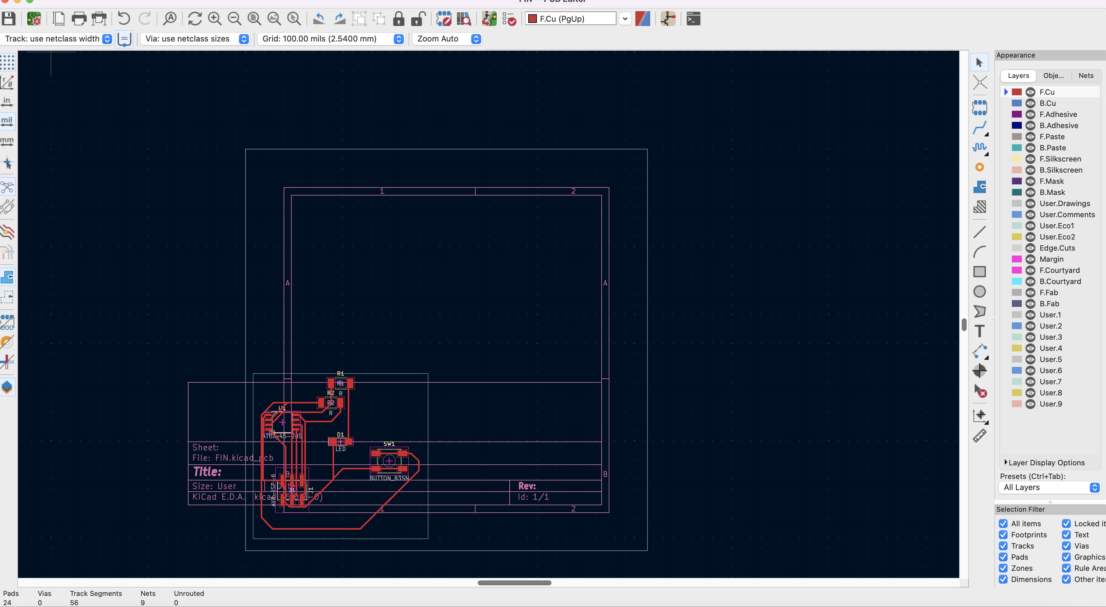
I have to make footprint to every components i have used during design the file should be in SVG
 .
.
Then open mod here
open rml file in GIMP SOFTWARE
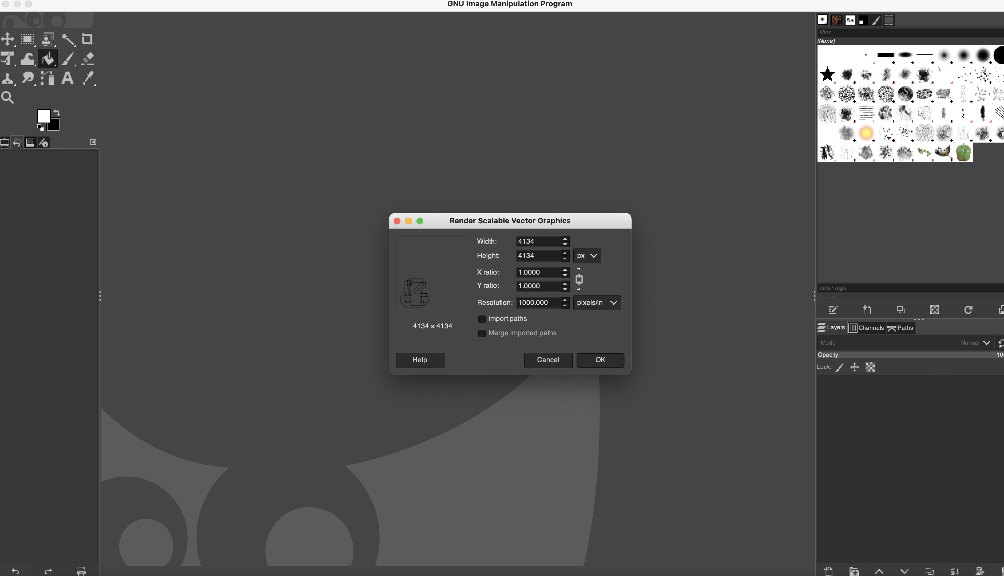
after exporting we should save image in png
Edge-cuts png in link to change in rml file

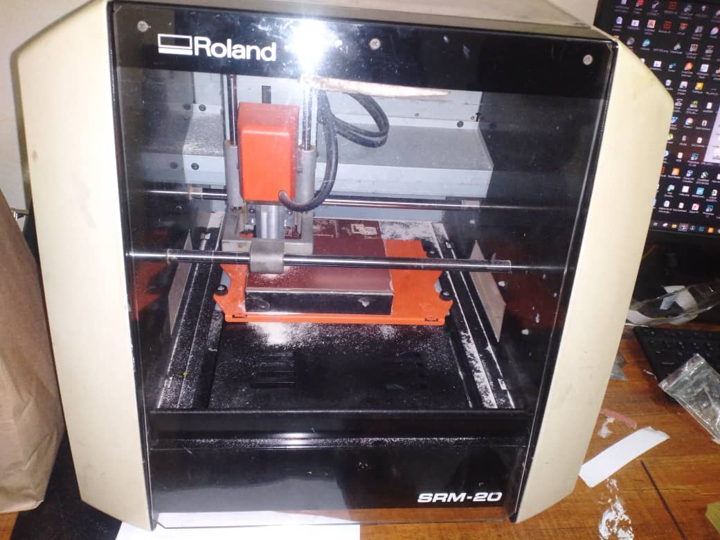
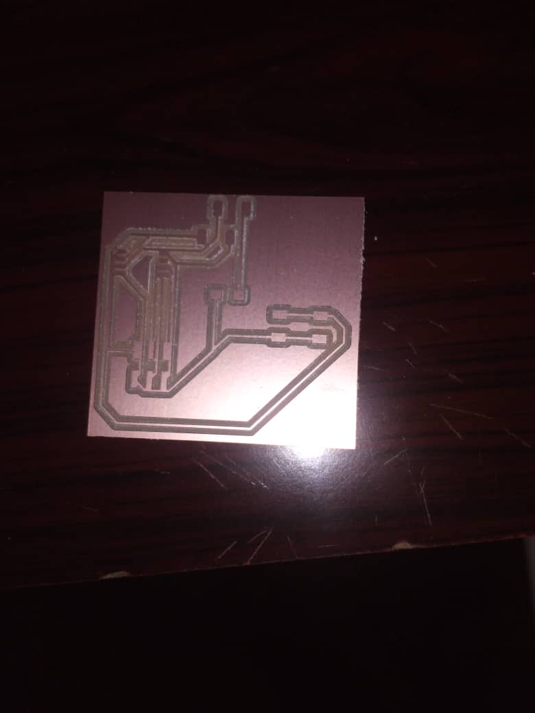
code in mods Then I passed the svg to mods to create the rml for the Roland, I was able to make the milling of the paths without problems
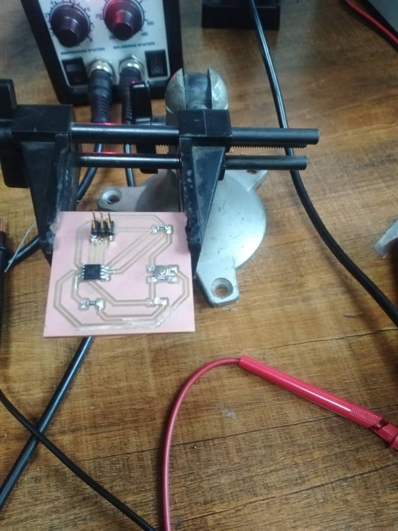
 The result of my design HELLO-World
LIST OF EQUIPMETS
| no | component | pieces | description |
|---|---|---|---|
| 1 | ATtiny45 | 1 | It is the processor and the circuit. |
| 2 | Push button | 1 | This will be the input part of the circuit. |
| 3 | LED | 1 | This will be the output part. |
| 4 | Resistor | 2 | It is used to limit the voltage on the LED |
| 5 | AVR ISP | 1 | It is used to program the ATtiny chip. |
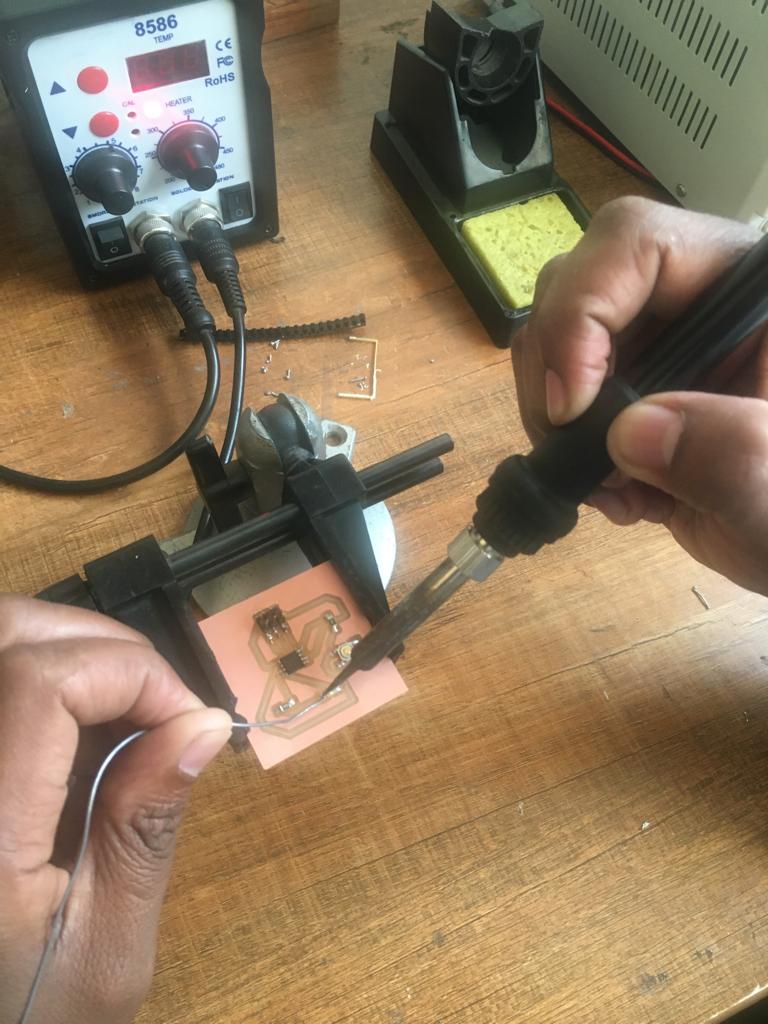
soldering
after testing the continuite and removing the error
Download file Download file kicad