5. Electronics production
Overview
This week we are going to explore about the Electronics Production which helps us to convert ideas to real world Products especially hardware. So it is necessary today if we want to control anything smart it required a smart hardware which perform well.There are many type of electronics production techniques available depends of the scale of the product
Work to be done Characterize the specification of yout PCB production process Make an In-circuit programmer by milling the PCB (program it, so I can use it).
Basic electronics production steps:-
- Design the Idea to a Schematic
- Create PCB Layouts from the Schematic
- Make PCB (Printed Circuit boards) from the Layout
- Assemble the components on the PCB using Soldering
- Testing and Finishing
- basic Electronics production steps are given above.
So we are gonna learn and do how Electronics Productions are done in FAB lAB and which methods are using
For this assignment the Design and Layouts are already given so we don’t have to make a design one.Instructed to make a In ‘circuit Programer’ as Individual assignment.The PCB production method I know is the chemical etching method but FAB Foundation not supports that method much because of the safety issues. So in FAB LABs We relay PCB Milling method for creating Prototyping PCBs
Milling machine
For PCB Production we use the milling machining method in fab labs which lets a person to make a PCB prototype like printing on paper using a paper printer so for PCB milling the FAB LAb provides a roland MDX 20 3 axis milling Machine.its a normal milling machine which we can also use for making PCBs
What should I learn this week
Group assignment
- Characterize the design rules for your PCB production process: document feeds, speeds, plunge rate, depth of cut (traces and outline) and tooling.
- document your work (in a group or individually)
Individual assignment
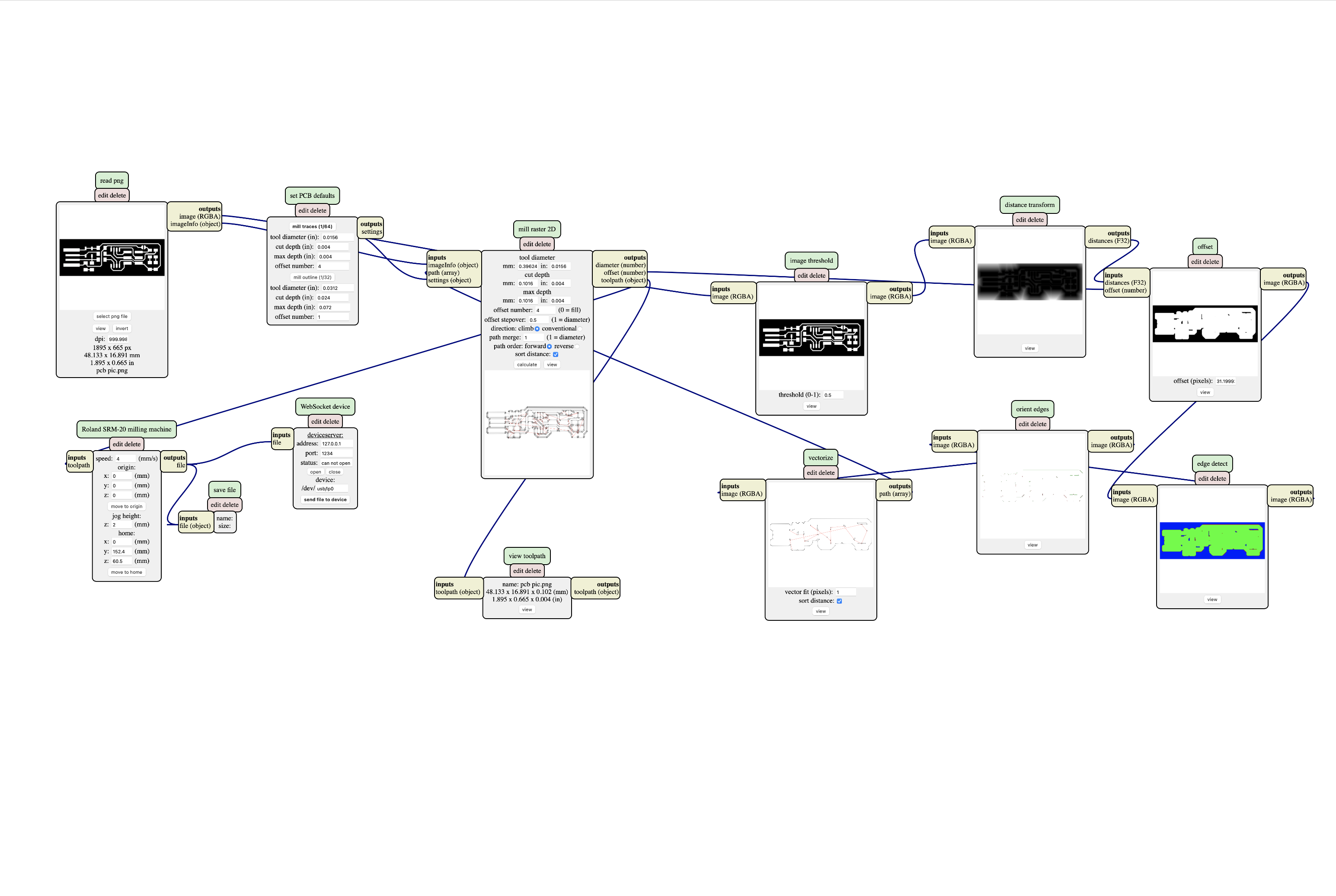
Make an in-circuit programmer by milling and stuffing the PCB, test it, then optionally try other PCB fabrication process. __ * Turn on the mill * Start mods with bash mods * Check that the mill head is in the raised position. * Remove and insert the drill bit that you want to use. * Turn on mods after starting the machine. * Load your SVG or PNG. * Check settings, make sure that your cut depth is not larger than the bit width / 2. * Move the drill bit to the origin, and try to find your starting point. Remember the coordinates. * Optionally, you can calibrate the mill height at different point on the plate and move back to the starting coordinates. * Carefully lower the milling bit and use your finger to stabilise the bit while tightening.
Learning outcomes
- Described the process of milling, stuffing,
- Demonstrate correct workflows and identify areas for improvement if required
selct head/ place
- server mods
- open program -> PCB milling -> 3.open socket/ open port
- open png
- set traces setting
- set origin/ cut speed move z axis manually
- calculate, check view
- send file 8 mill…
In this asignment I will be using design found in Brian’s work on designing the FabISP.The following are images I used for milling the PCB.
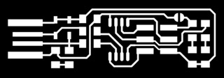
The above image is for traces for FabISP.
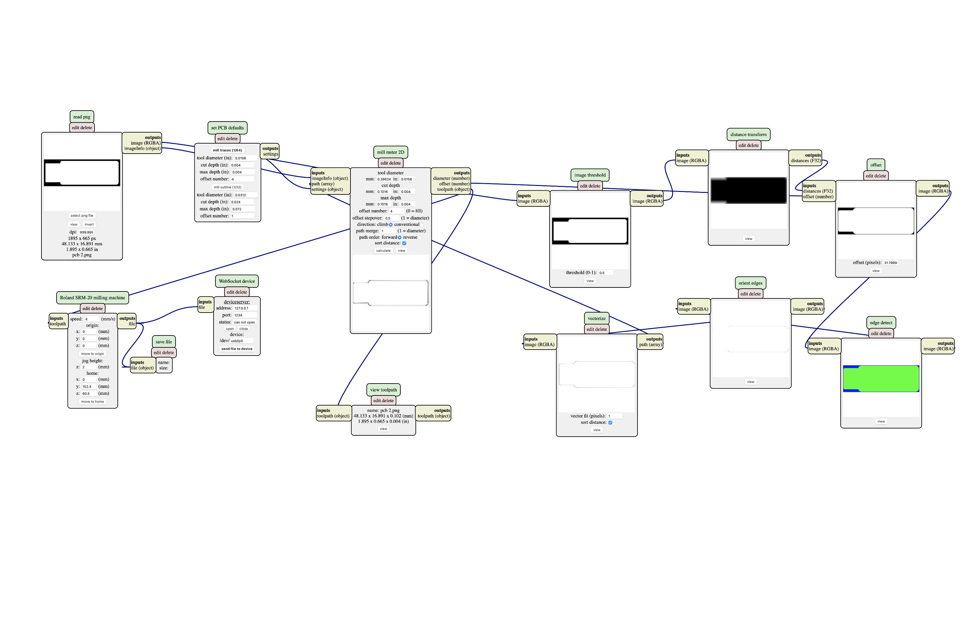
 The bellow image is for edge cut of FabISP.

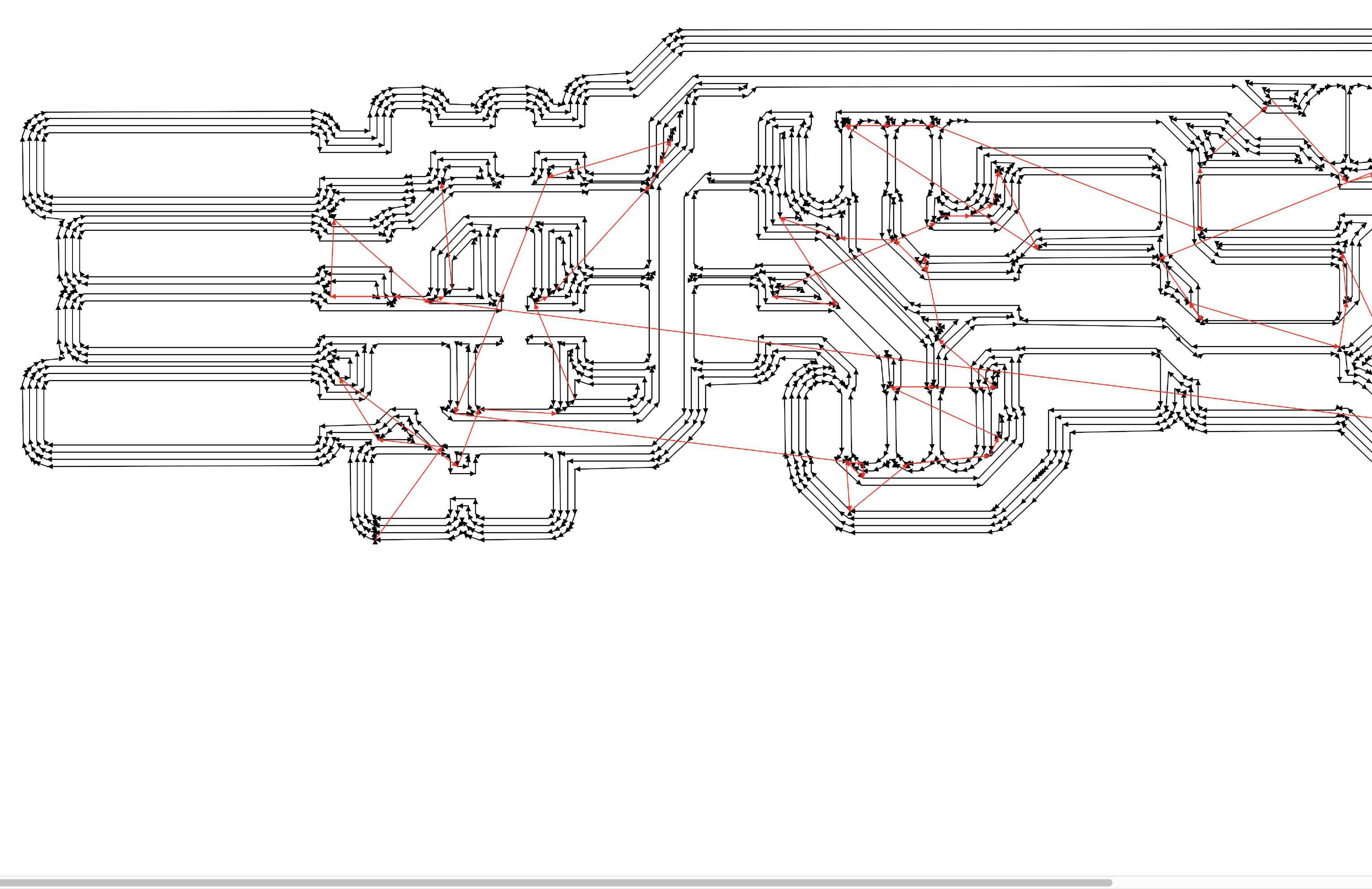
 After calculating the path for the tool the RML file is generated.
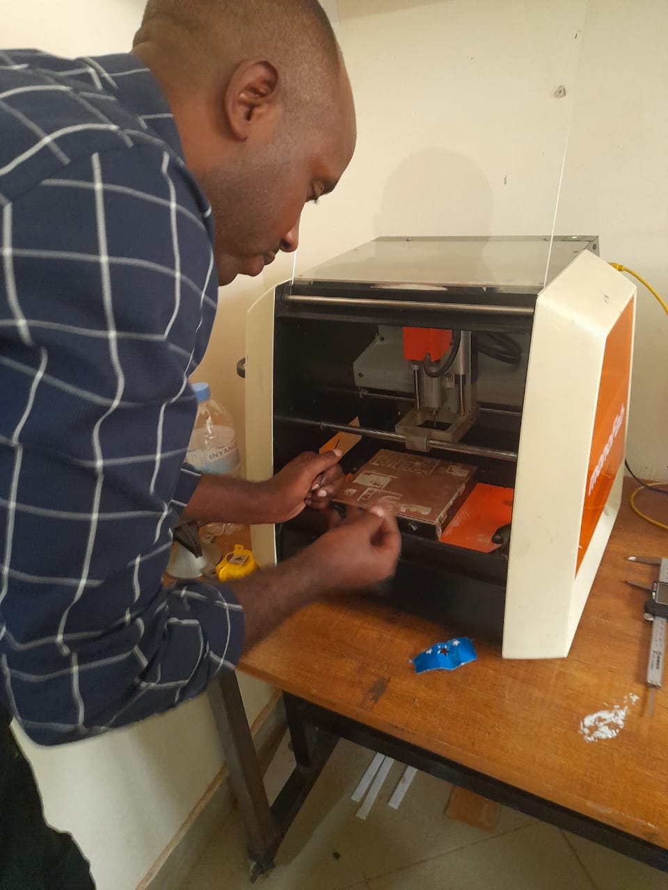
 we have SRM-20 monofab milling machine.
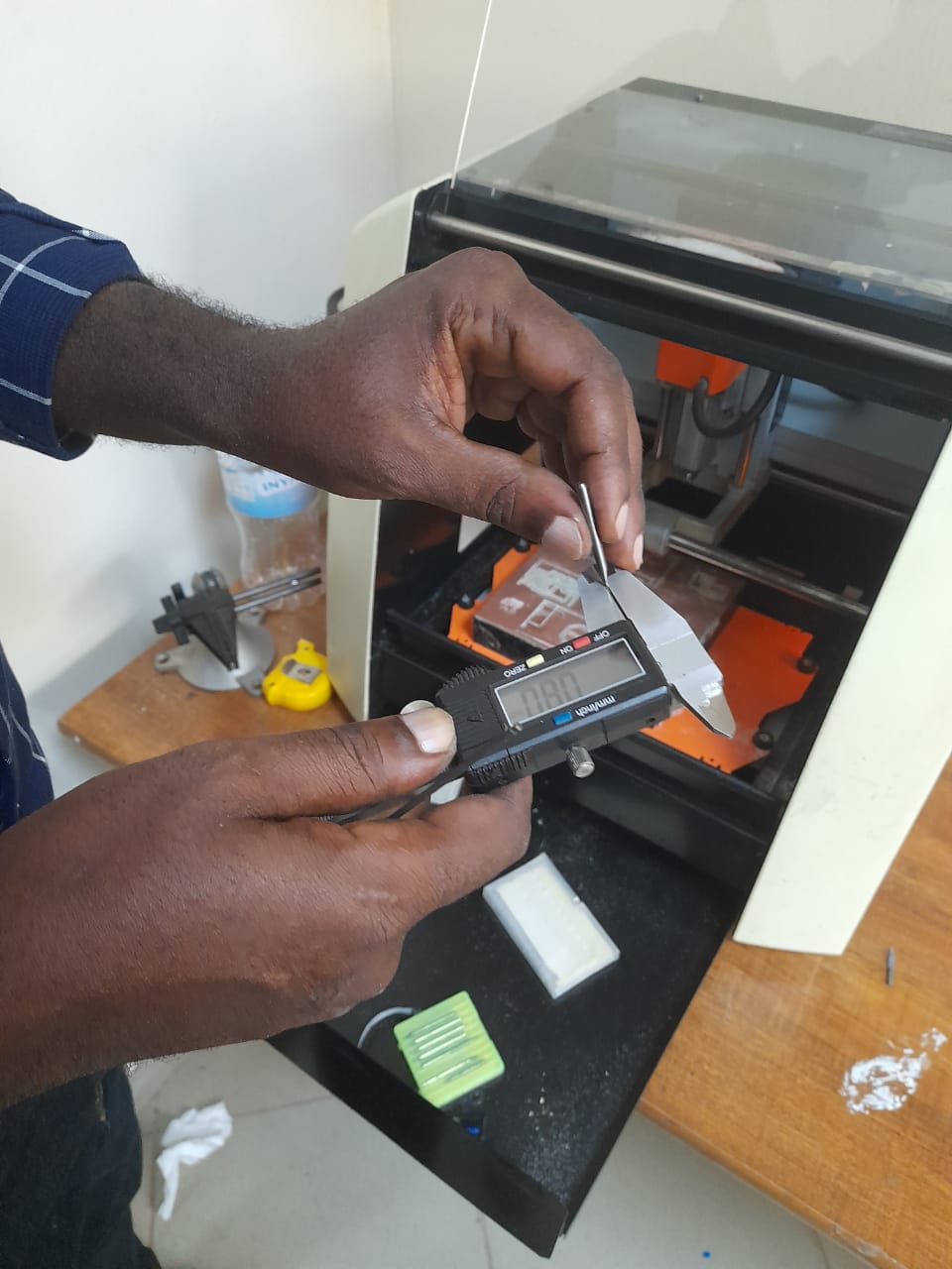
 measuring the mill bit for edge cut
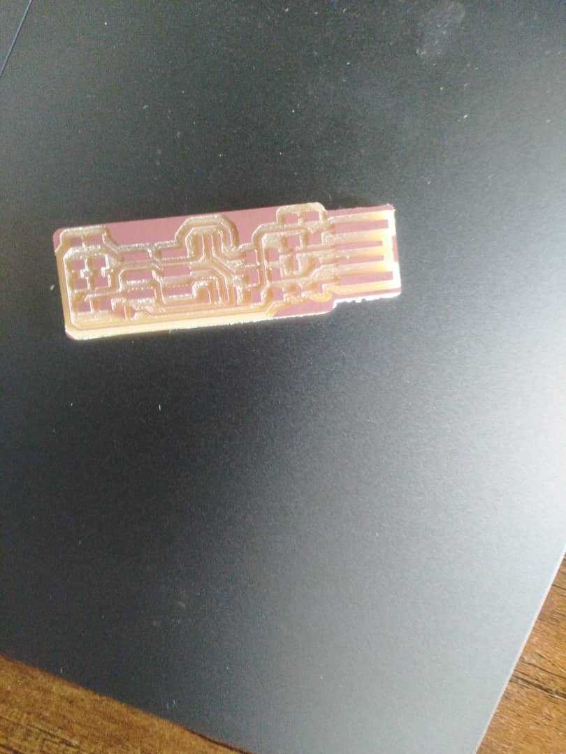
After making the rml with mods the result was very bad then i tried again to make it very good
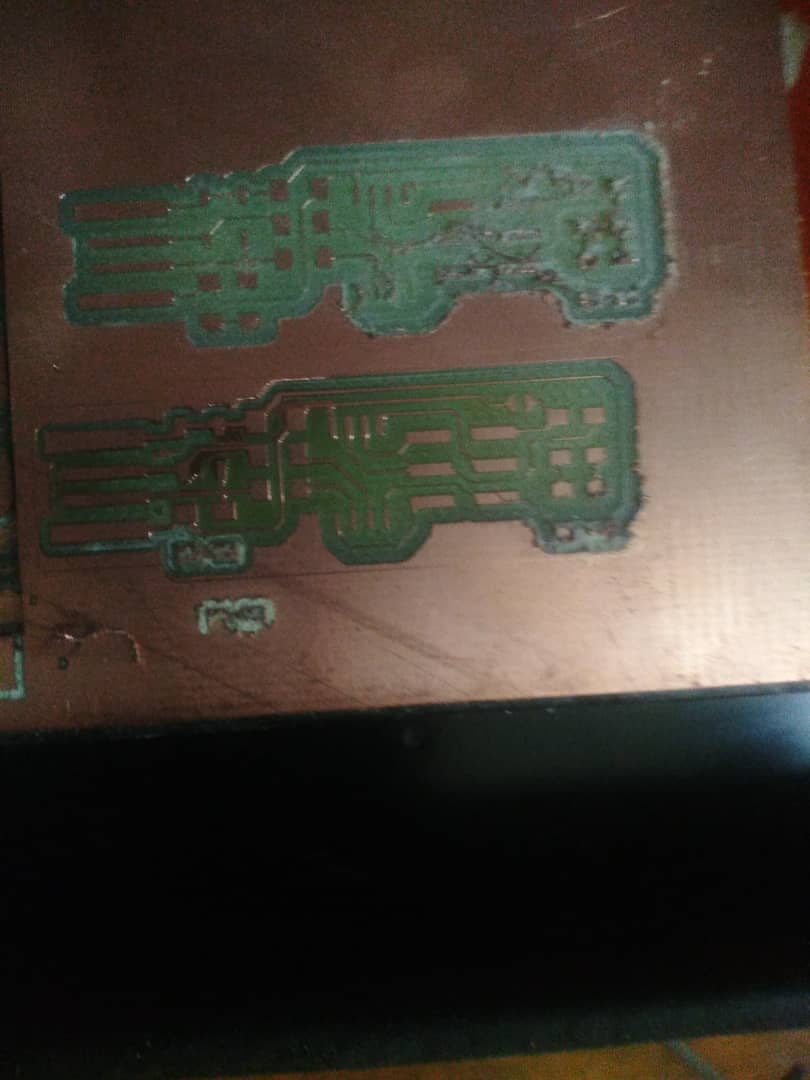
This the result after fixing it and correcting the mistakes i did before
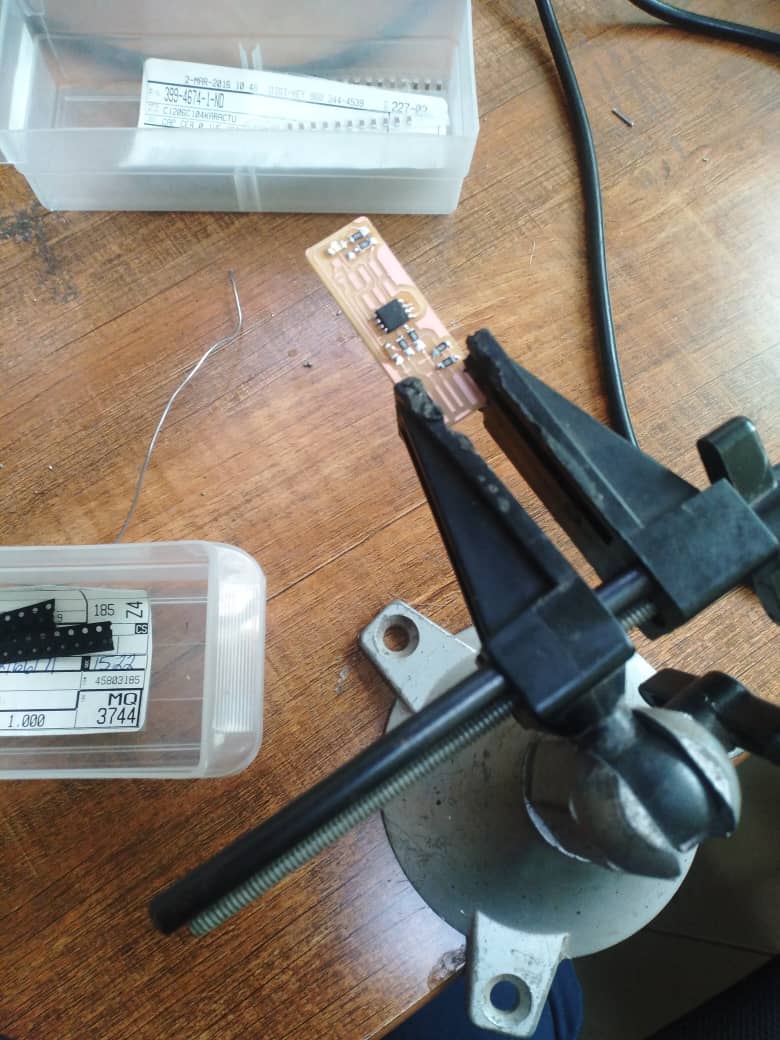
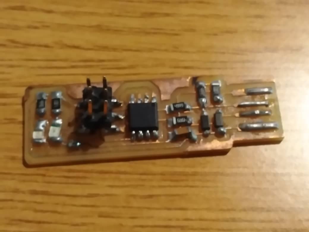
Solder components to the board
With the good board, 0.5mm diameter tin, the thinnest tip of my soldering iron and a temperature of 200-210 º (Thanks again Fred and Rembert) I’m back to try to solder the components to the board
| no | component | Pieces |
|---|---|---|
| 1 | ATtiny45 | 1 |
| 2 | 1 Kohm | 2 |
| 3 | 499 ohm | 2 |
| 4 | 49 ohm | 2 |
| 5 | 3.3 zener | 2 |
| 6 | Red LED | 1 |
| 7 | Green LED | 1 |
| 8 | 100nF. | 1 |
| 9 | 2x3pinheader | 1 |
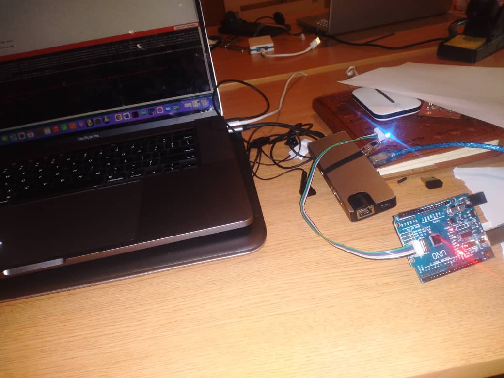
Program the programmer
I tried to program the programmer by following the tutorial of brian
1.Connect programmer to computer
2.check connection of programer and computer if it is connected well
First step I did: run nano Makefile to change the Programmer into “atmelice_isp” as instructed in Brian’s tutorial. second step: download the firmware to be loaded in the programmer. Then run make flash in terminal to erase the target chip.
run make flash
it says avrdude -p attiny45 -c atmelice_isp -P usb -e -U flash:w:fts_firmware.hex,
make fuses
last step:
-
Disconnect the programmer and connect ATtiny board and it recognized as Multiple Vendors
USBtiny, -
check it by running the command
lsusbit should list all the usb on your computer.
Have you?
- Linked to the group assignment page
- Documented how you made (mill, stuff, solder) the board
- Documented that your board is functional
- Explained any problems and how you fixed them
- Included a ‘hero shot’ of your board
From Youtube
Download the tutorial i followed to design using software here