Leen Nijim
Assignment 7
Electronics Design
Task
Our task this week was to redraw, make and test one of the Hello-World Boards and add at least an LED and a push button.
What You Need
- Access to a PCB mill.
- A couple of PCBs.
- Access to a soldering station.
Files to Download
- Hello board ATtiny44 KiCAD.
- Hello board ATtiny44 cutout png.
- Hello board ATtiny44 holes png.
- Hello board ATtiny44 traces png.
- Hello board ATtiny44 blink code.
Hero Shots
Group Assignment
For our group assignment, please click here.
Making Hello-World Board ATtiny44
Preparing the Schematic
For simplicity, and because I might be using such a board for my final project, I have decided to make a variation on the ATtiny44 board.

Setting Up KiCAD EDA
I started by downloading and installing KiCAD, and then proceeded to add the necessary Fab Academy components library from the GitLab repository after unzipping them into a local directory.
I then created a new project and named it helloBoardATtiny44 which automatically creates a schematic file and a PCB design file. The schematic file will contain the logical connections and the components my board will use, and the PCB file will contain the layout these components will have on the physical board.
The first step is then to open the schematic file and setup the properties of the sheet of paper I will be drawing my components and circuit on, which eventually could also be printed out or saved as a PDF. In these settings, I added a name to the circuit design and other data management information like my name and schematic revision number.
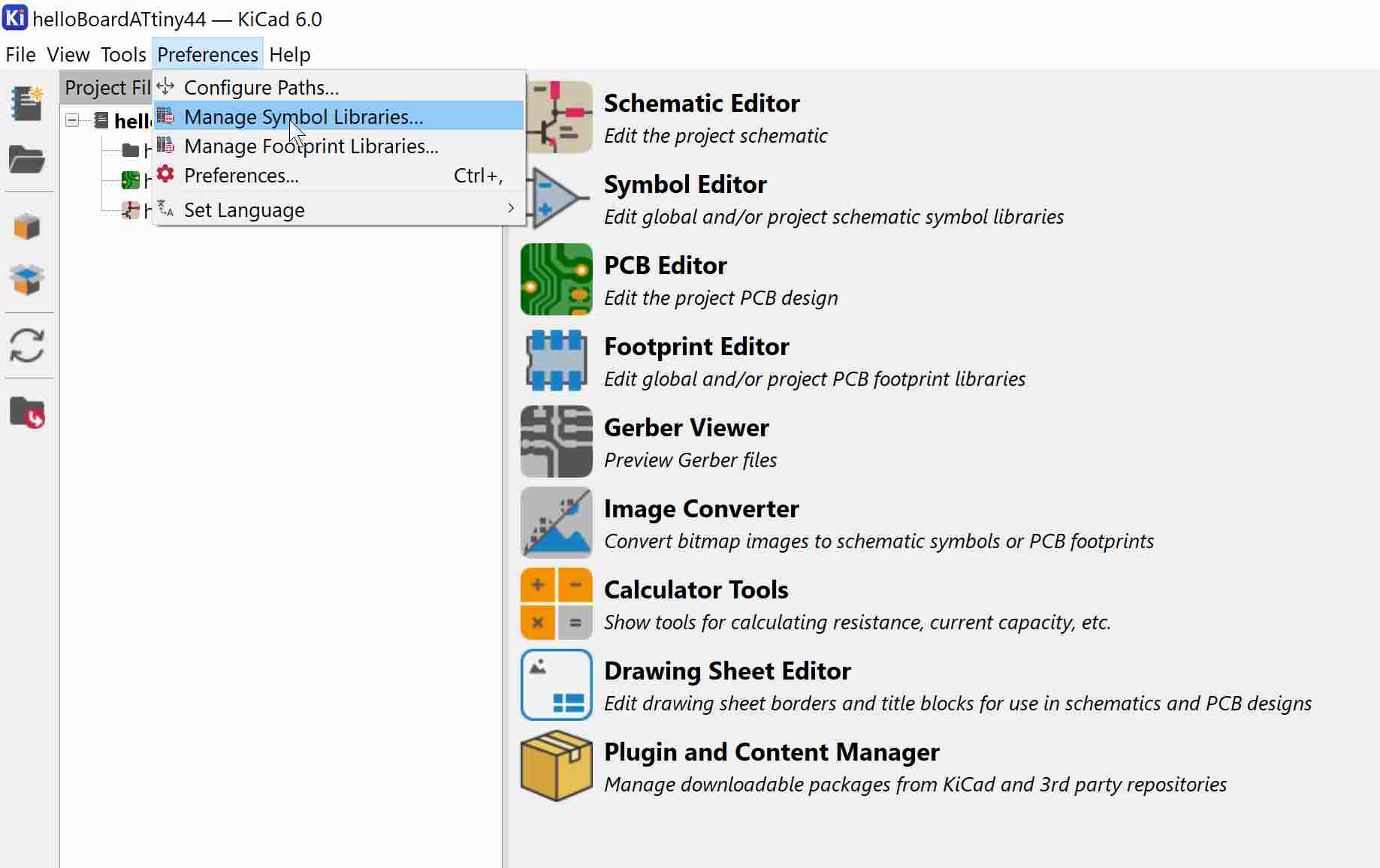
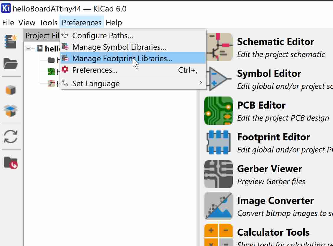
After that, I started adding the Fab library I downloaded to disk by going to Preferences > Manage Symbol Libraries.
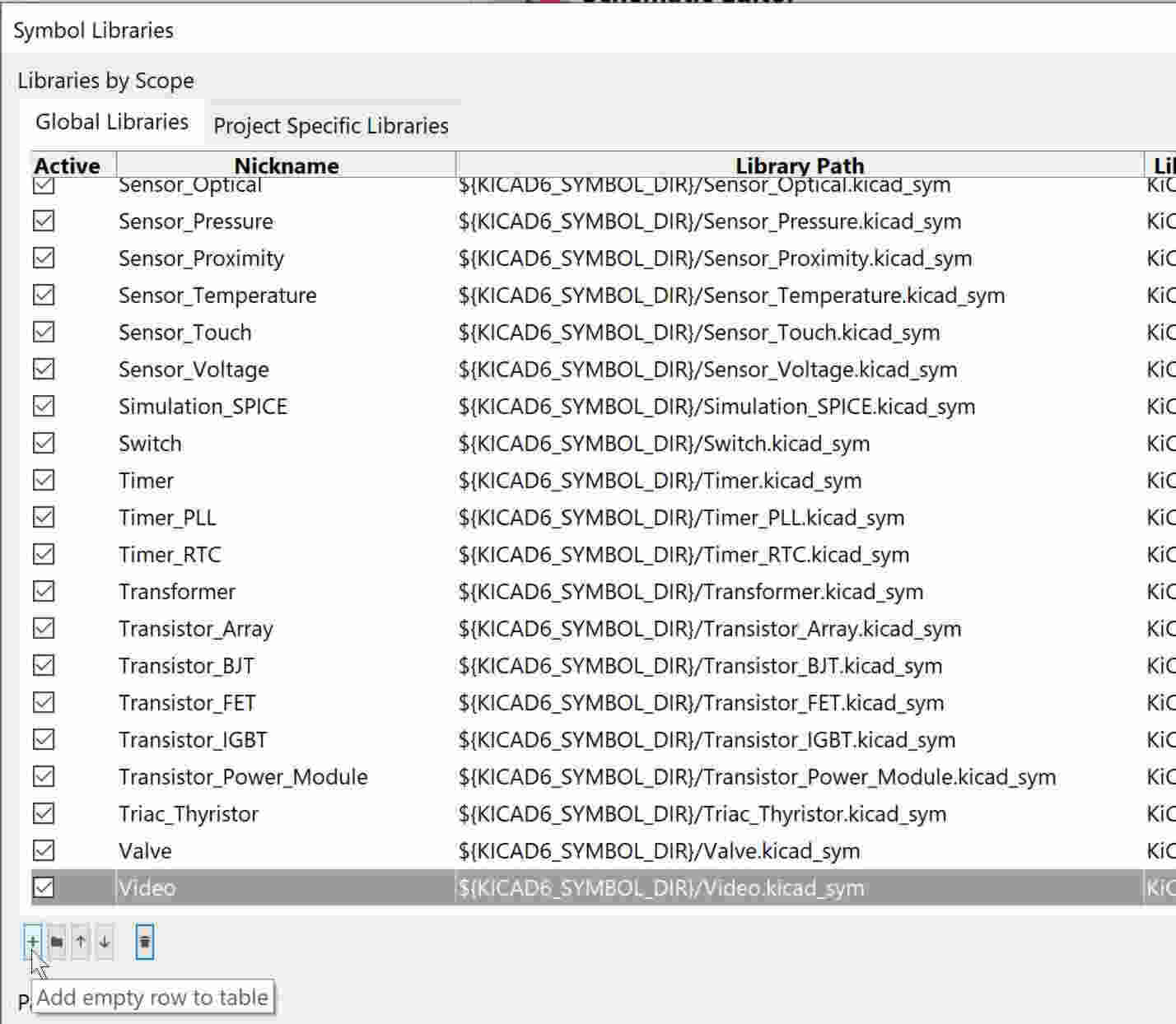
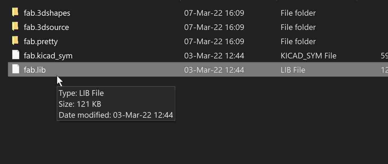
In there, I added a new entry, called it fab (keep in mind that these libraries are case-sensitive), and navigated it to the local directory of the fab.lib file.

Next came adding the footprints library that contains all the shape properties of each component and information about the physical copper pads needed for soldering them on a PCB.
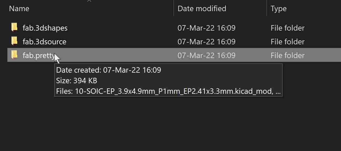
Here, I directed it to the fab.pretty folder.
With that done, I am now ready to start designing my circuit schematic.
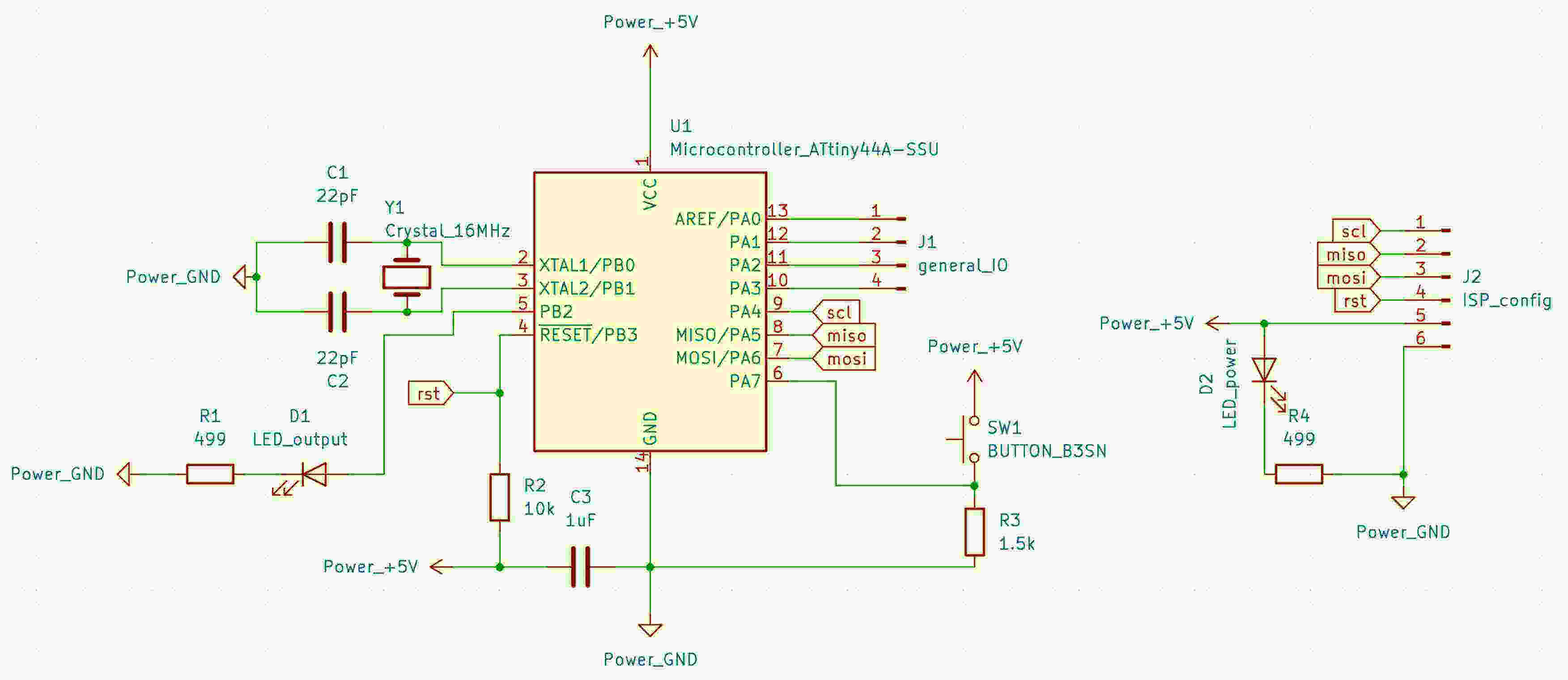
Desiging the Schematic File
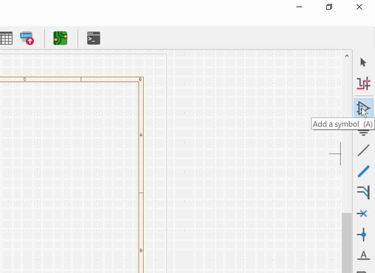
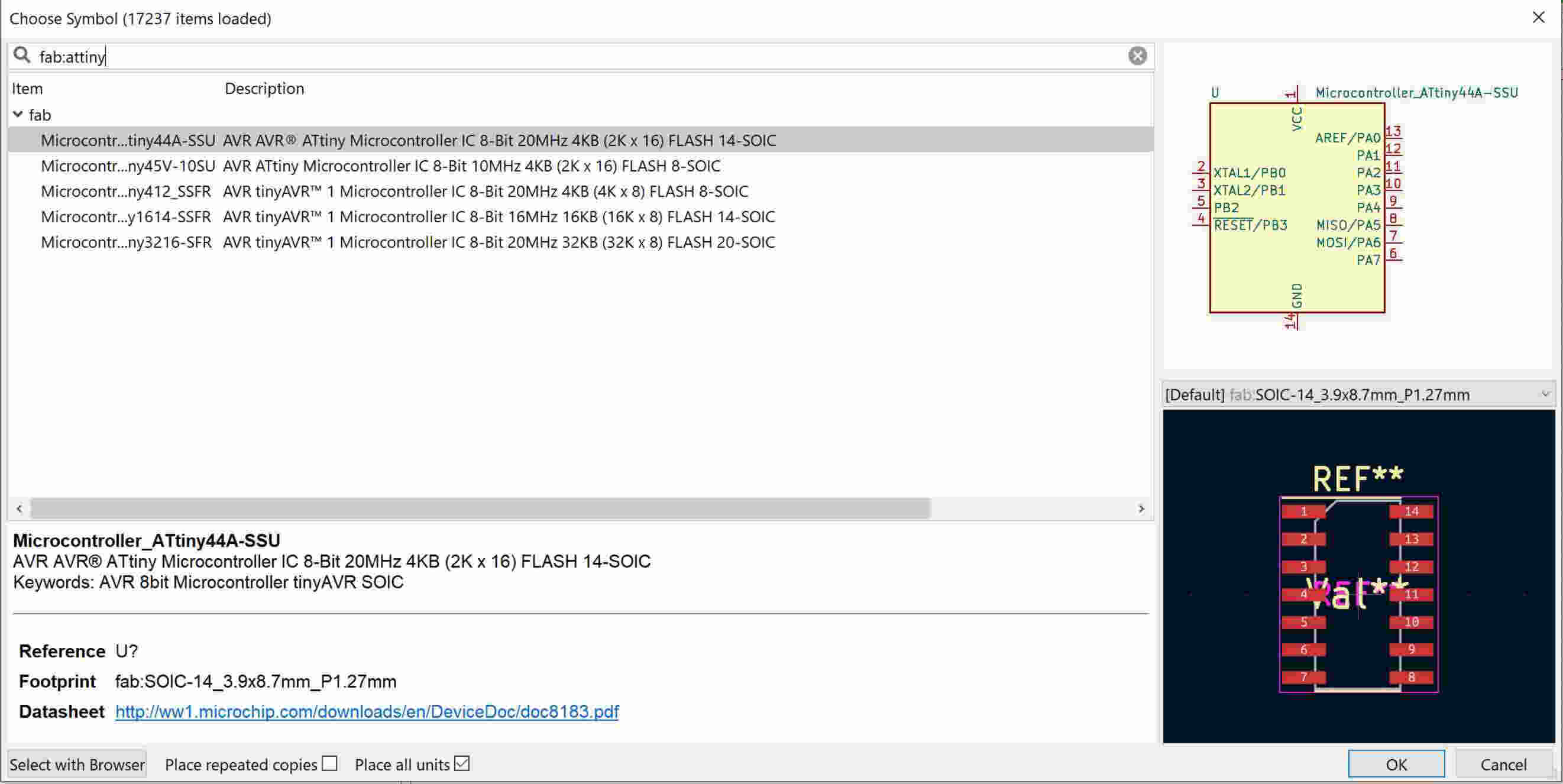
To add a component, I went to the right-hand function column and clicked on Add a symbol.
In there I typed in fab:attiny to limit the search for the microcontroller to the fab library I just added. And then placed the component on the schematic.
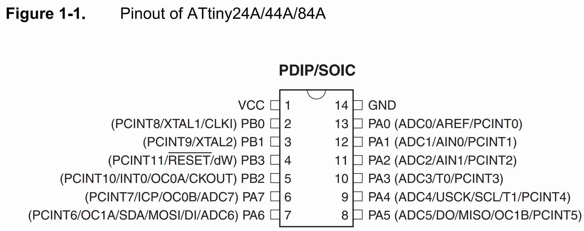
One the side, I had this schematic open to help me connect the pins to the appropriate components.
I later realized though that I do not need the colon to limit my search. So I continued adding the components I need and placed them on the screen.
.jpg)
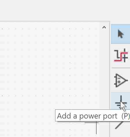
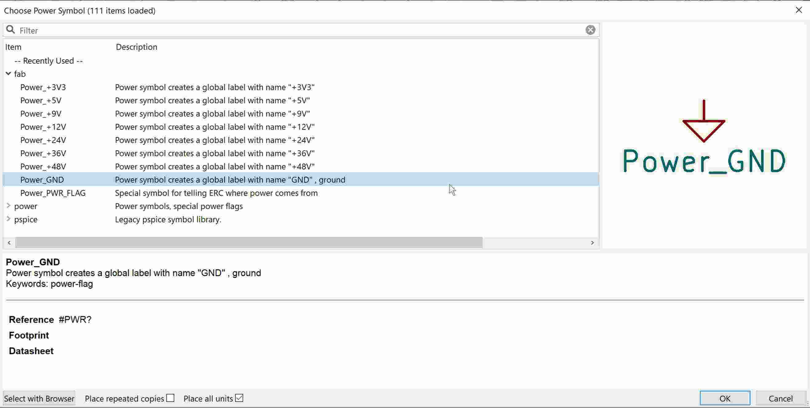
To add a power source or a ground connection I clicked on Add a power port and chose the connection I needed.
After I was done adding my components, I started to connect them logically using the Add a wire function.
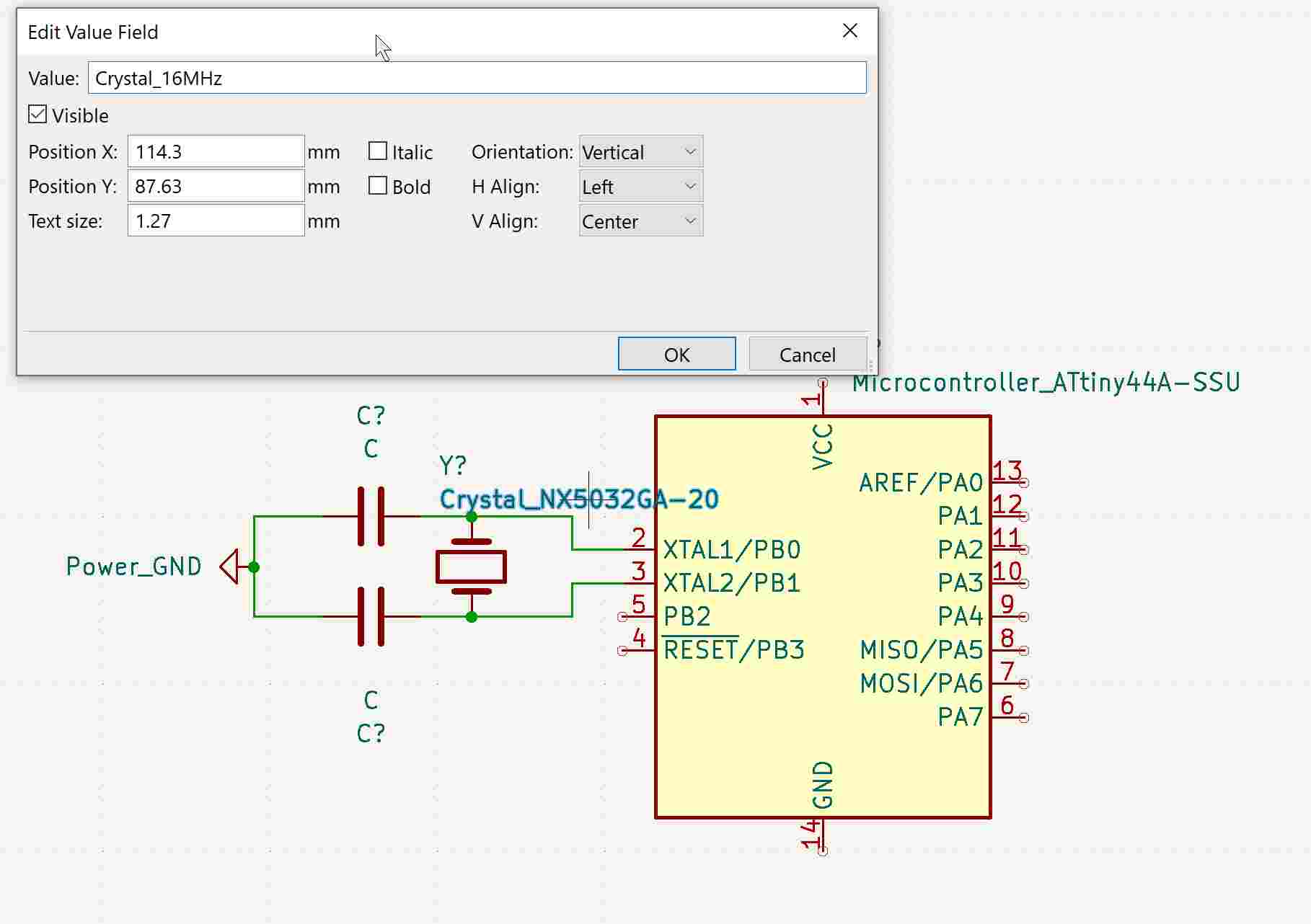
It was also good practice to give my components meaningful names by double-clicking the name tag and editing the entry.
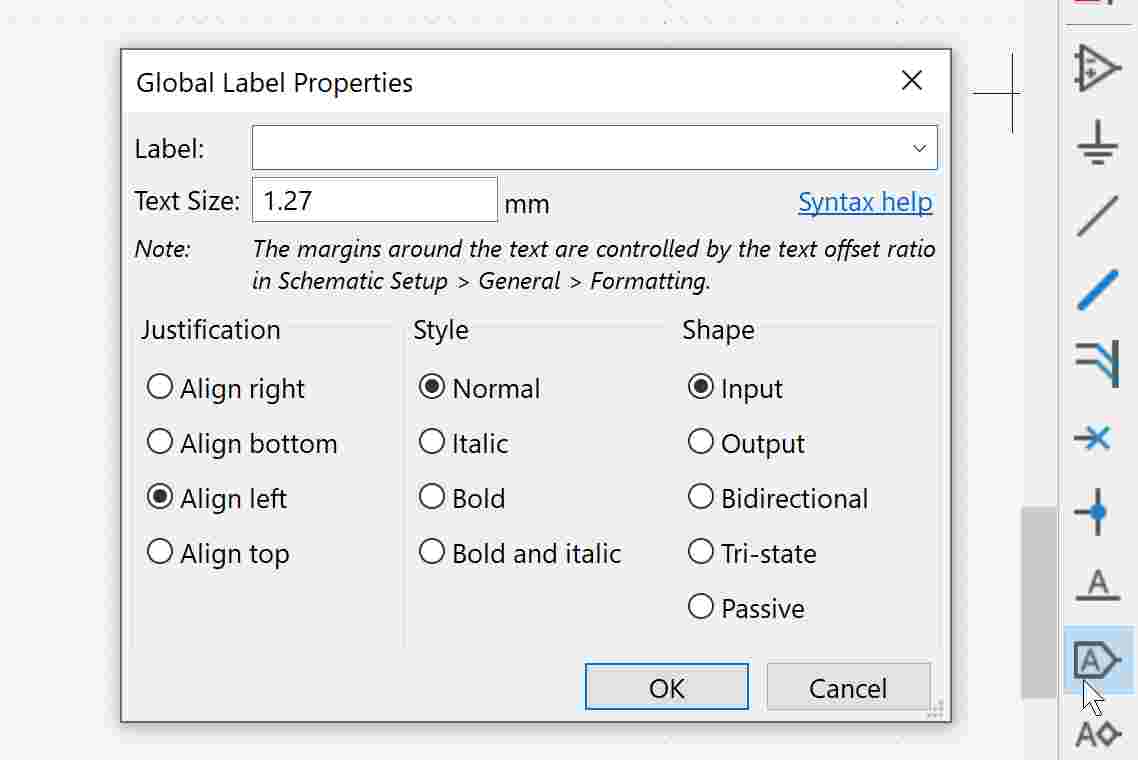
To avoid having to connect all wires between all the components (which could become messy for more complicated board designs), I used labels to name my connections and just added those labels where a wire would have to be physically connected.
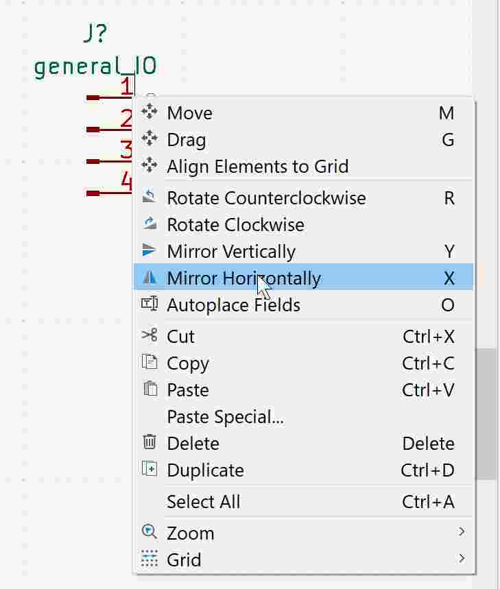
Another two functions I used when placing the components are the Rotate and Mirror functions.
After I was satisfied that all my components have been connected to the correct ports and pins, I used the Fill in schematic symbol reference designators function to automatically name the components that I did not actively name. This is important because I would not have been able to proceed to the PCB design otherwise.
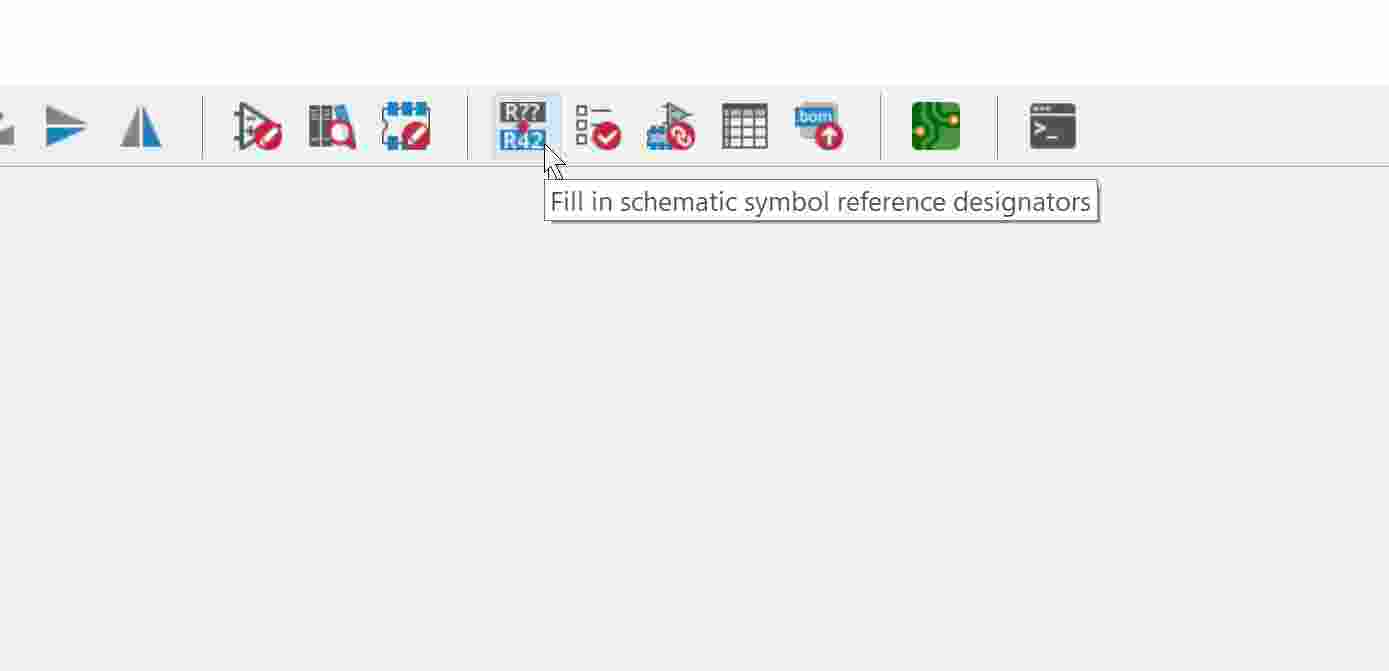
Every component has an appropriate annotation now.
Next step is to assign physical footprints to all components.
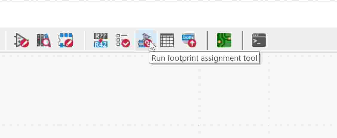
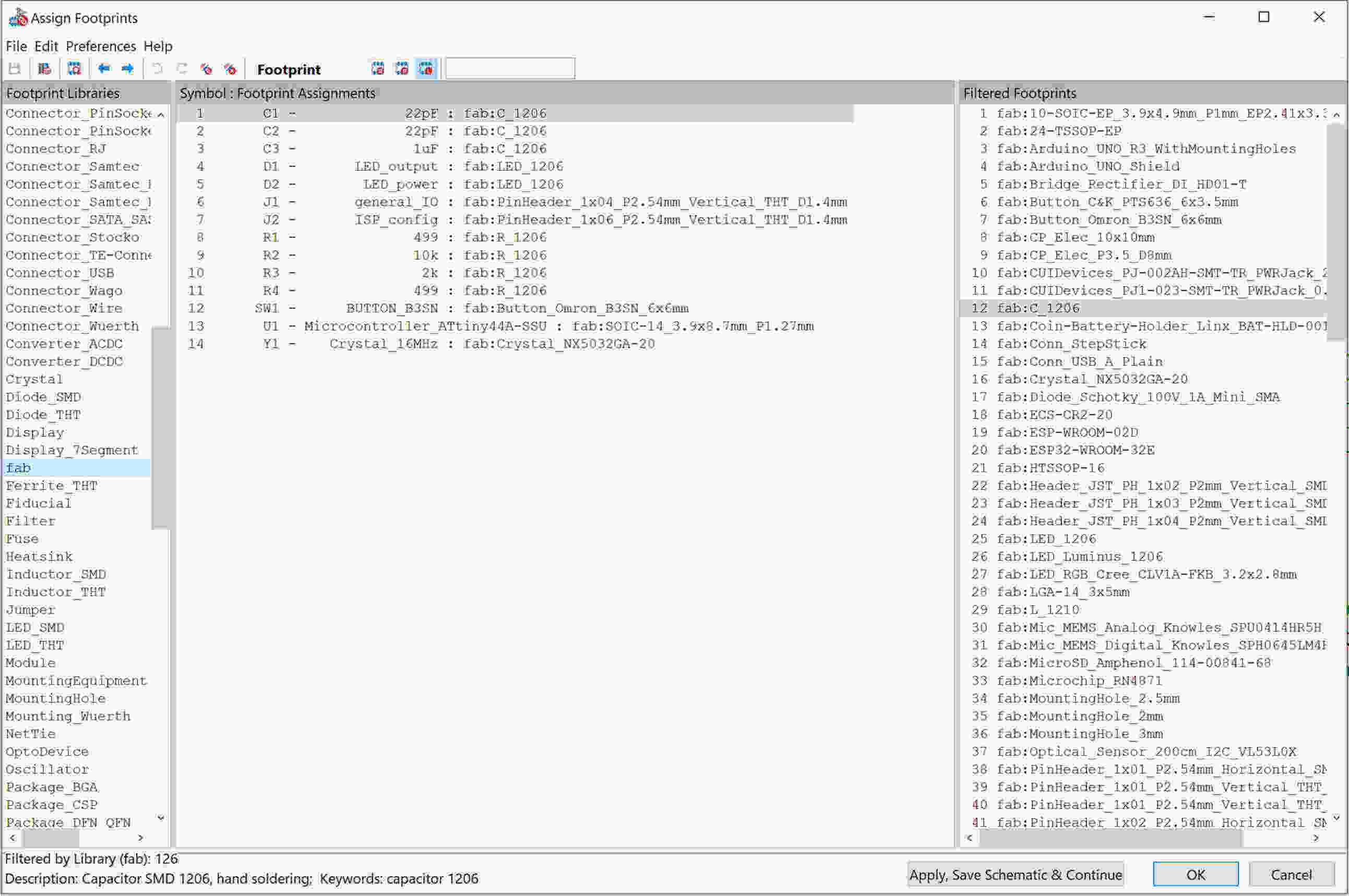
In there, I selected the fab library on the left and assigned each component to a footprint by double-clicking the selected footprint from the right side list.
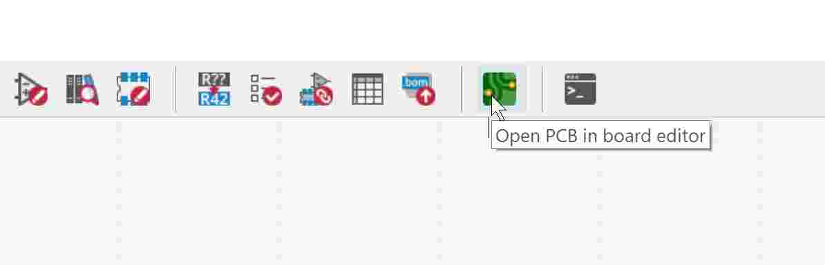
When I was done, I went to open the PCB editor by clicking Open PCB in board editor.
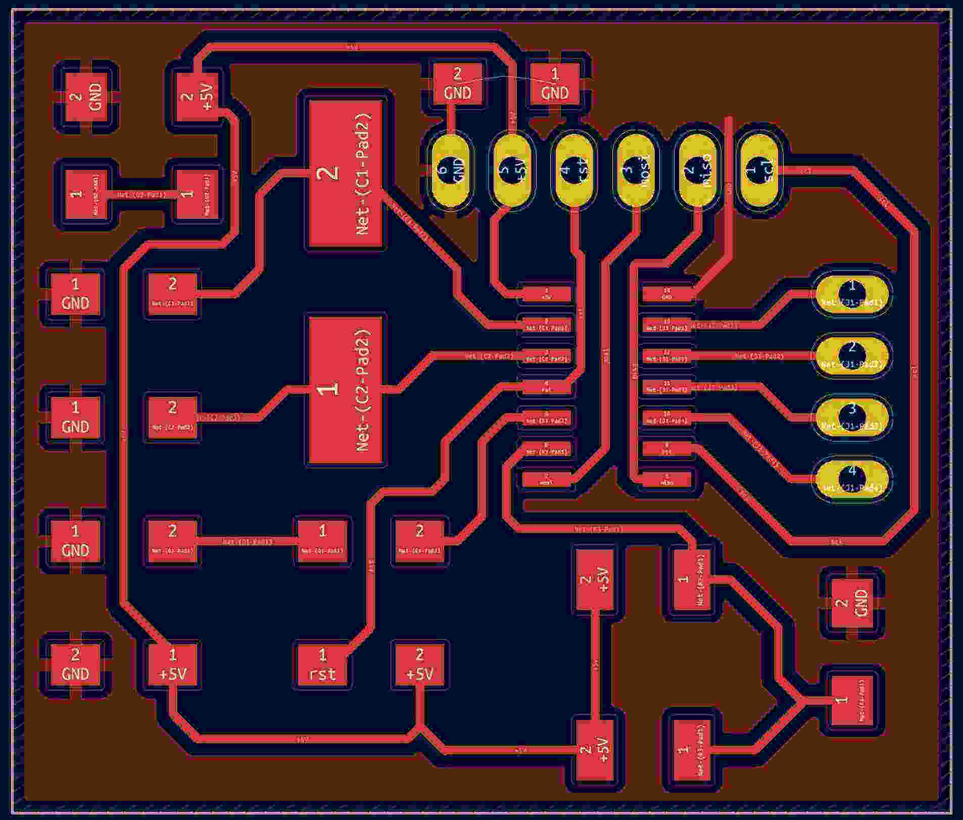
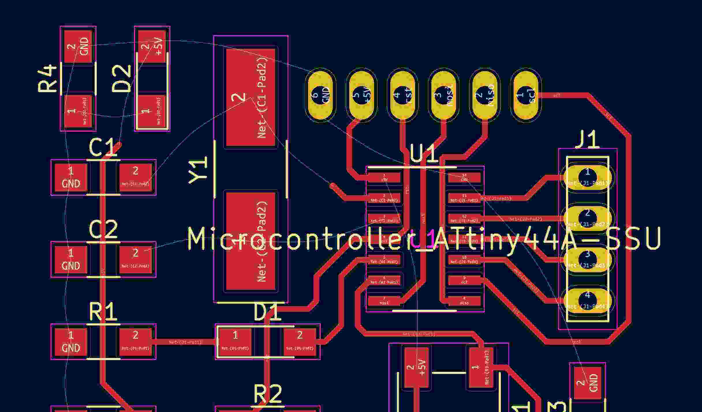
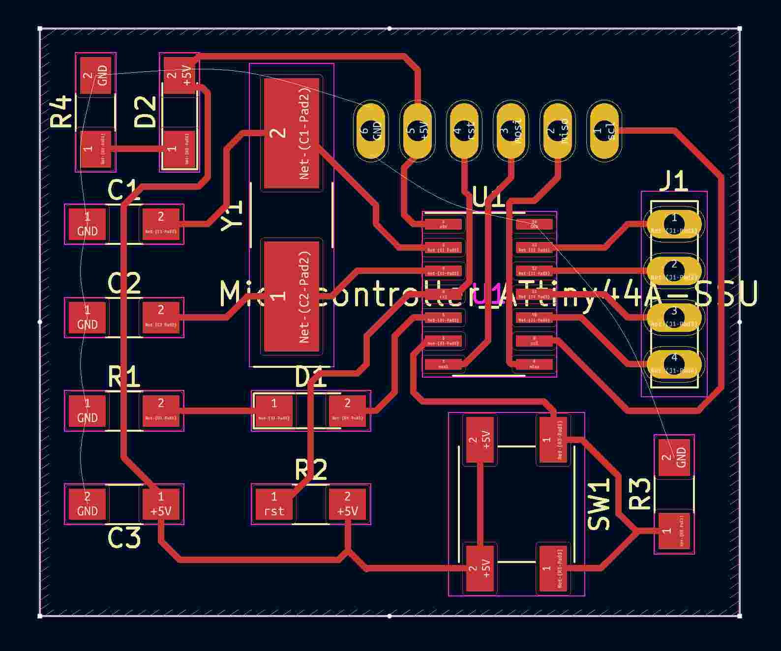
Designing the PCB Board
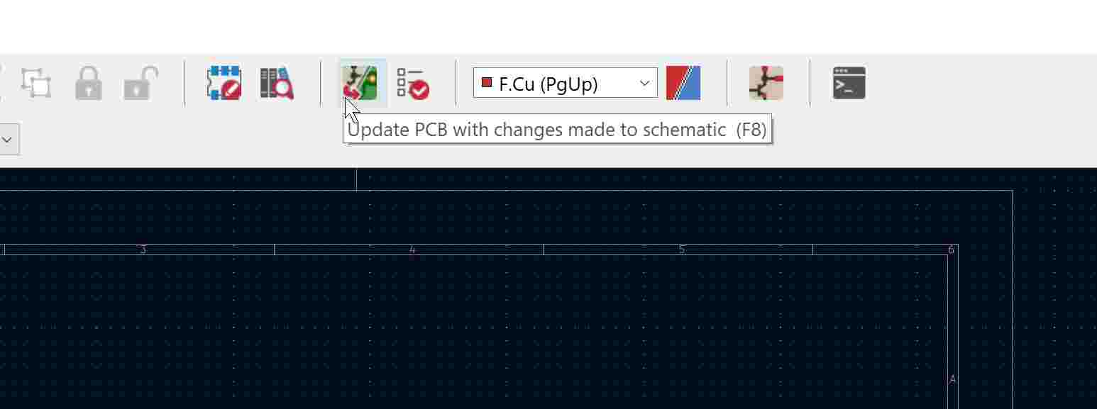
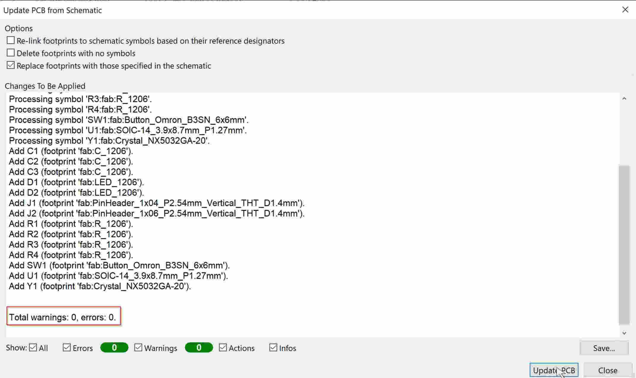
With the board designer open, I clicked on Update PCB with changes made to the schematic to add the circuit footprints.
After making sure I had no warnings or errors, I clicked Update PCB. Such errors can happen if the footprints were not assigned in the step earlier, or if there was a problem with locating the footprint library.
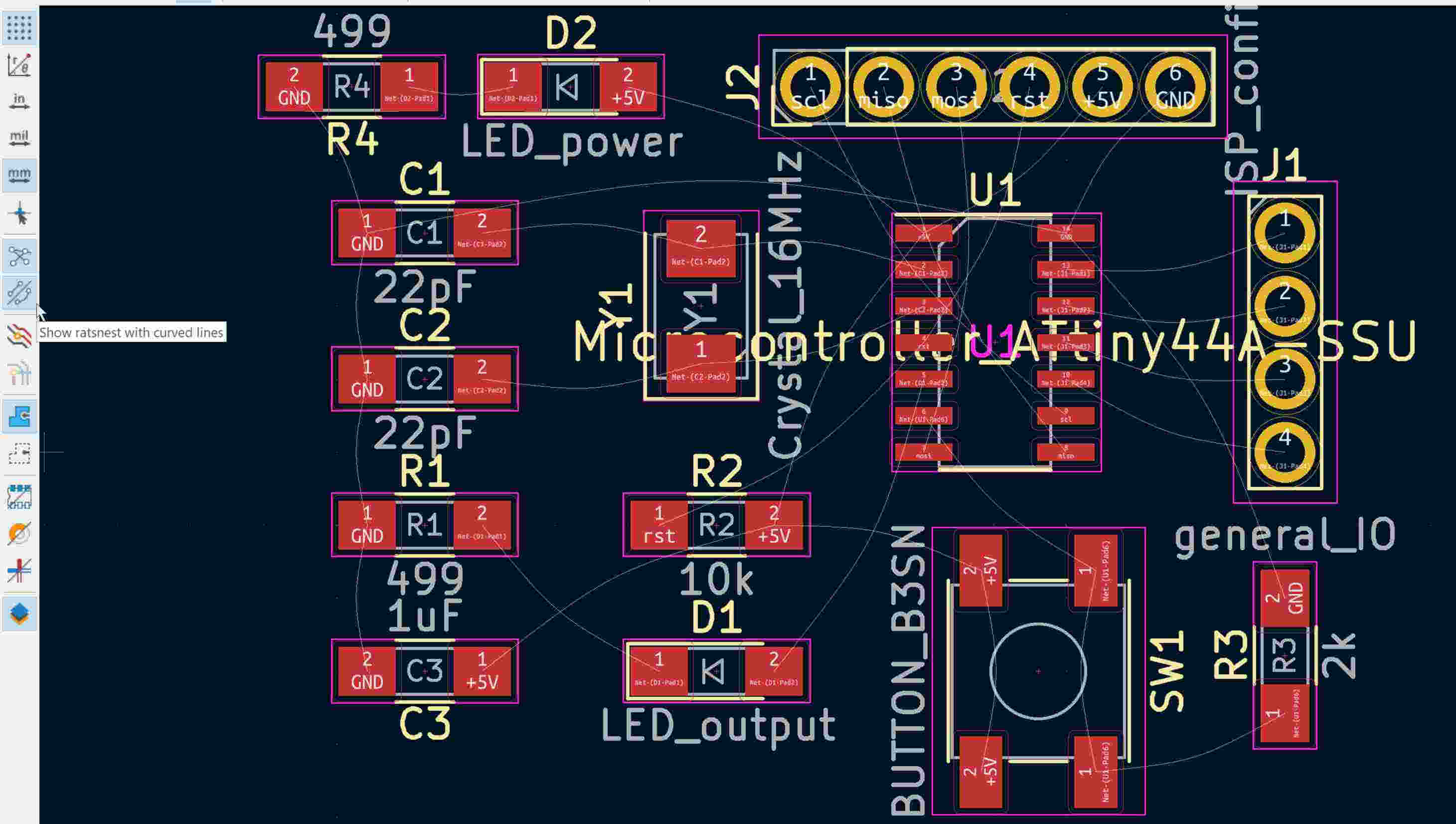
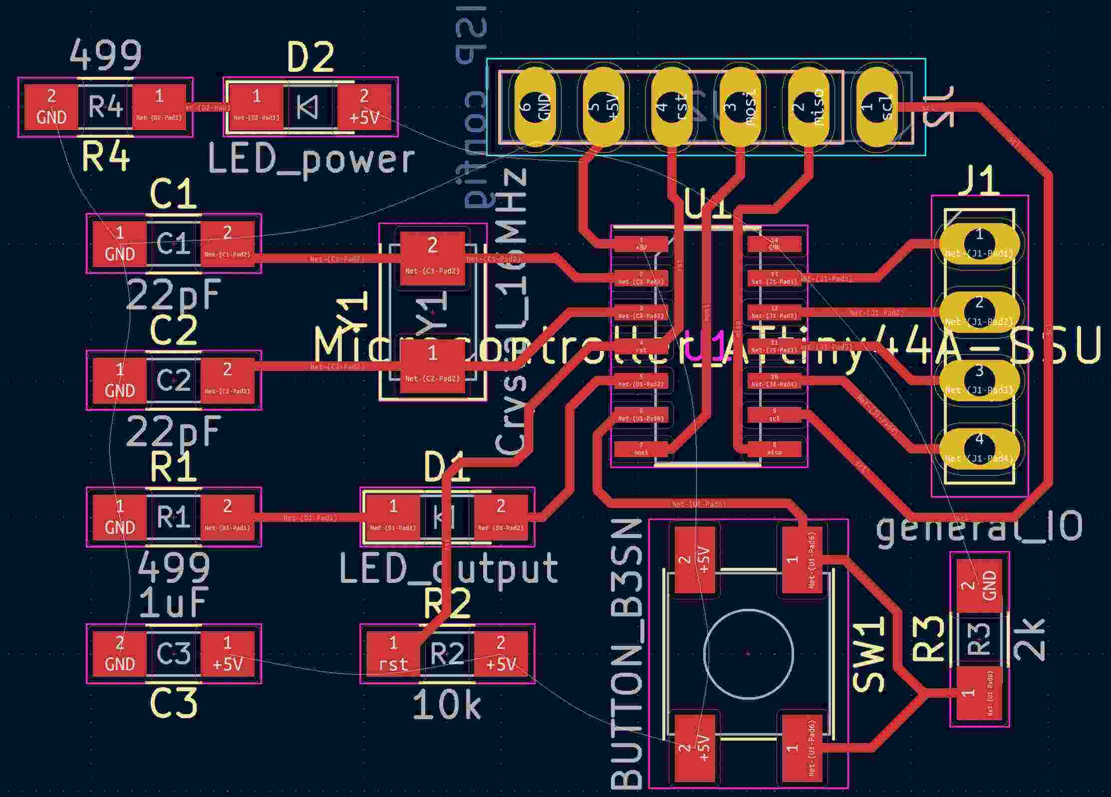
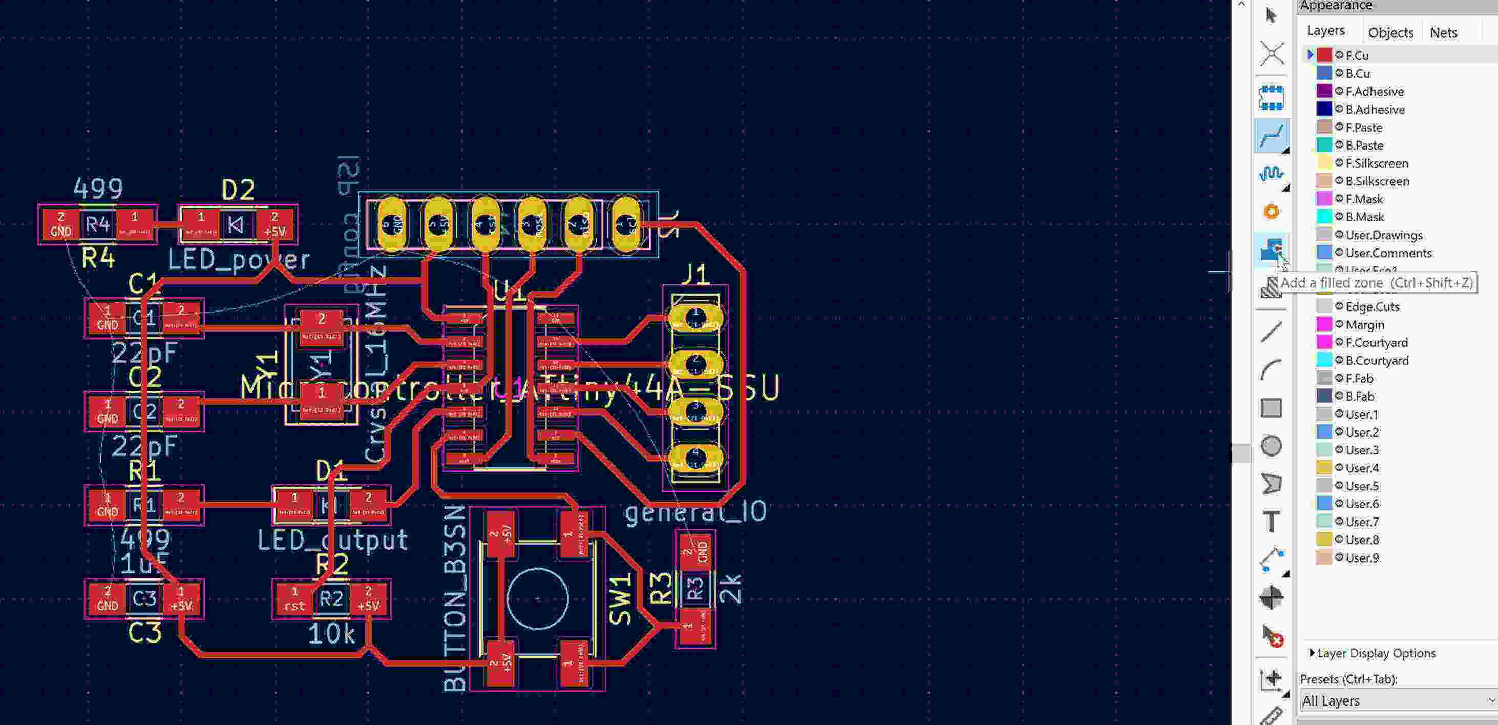
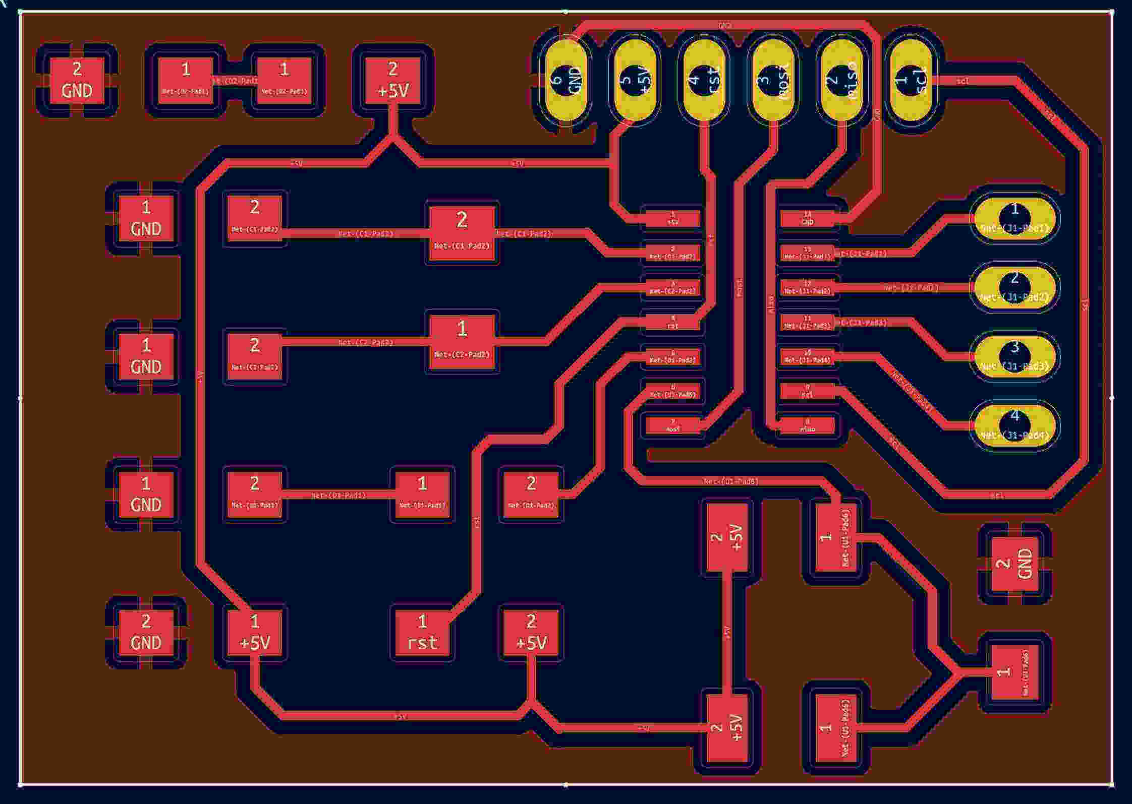
I now had all my components added with a ratsnest that shows me where to connect every single pad.
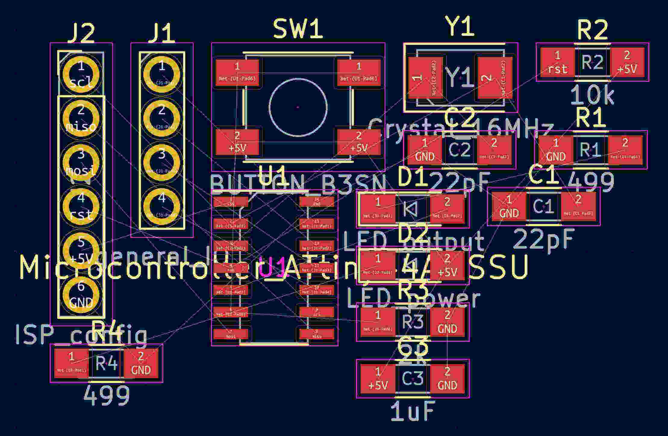
So I started moving things around and trying to find the best placements for each item. I used the keyboard shortcut R a lot to rotate items.
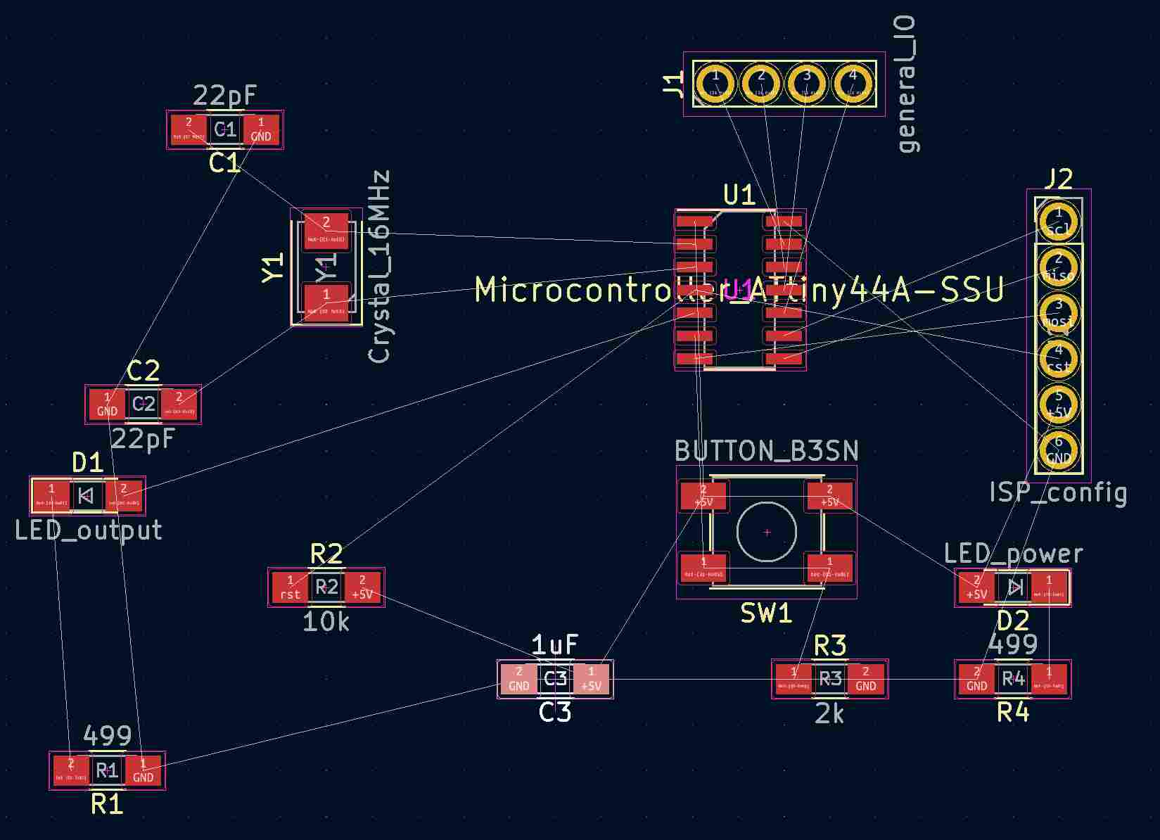
I also found switching the ratsnest to curved lines made it a lot easier to see the single connections that were otherwise lying on top of each other.
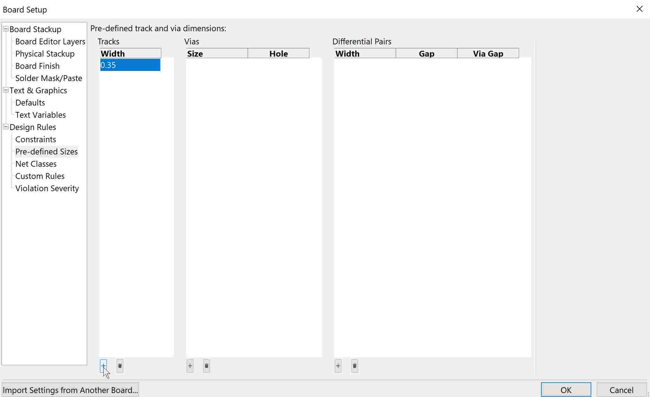
After I was satisfied with the placement, I went ahead and edited the design rules in preparation for milling.
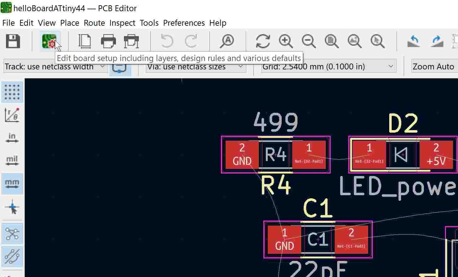
In there, I added a new Net Class and made the trace width thicker.
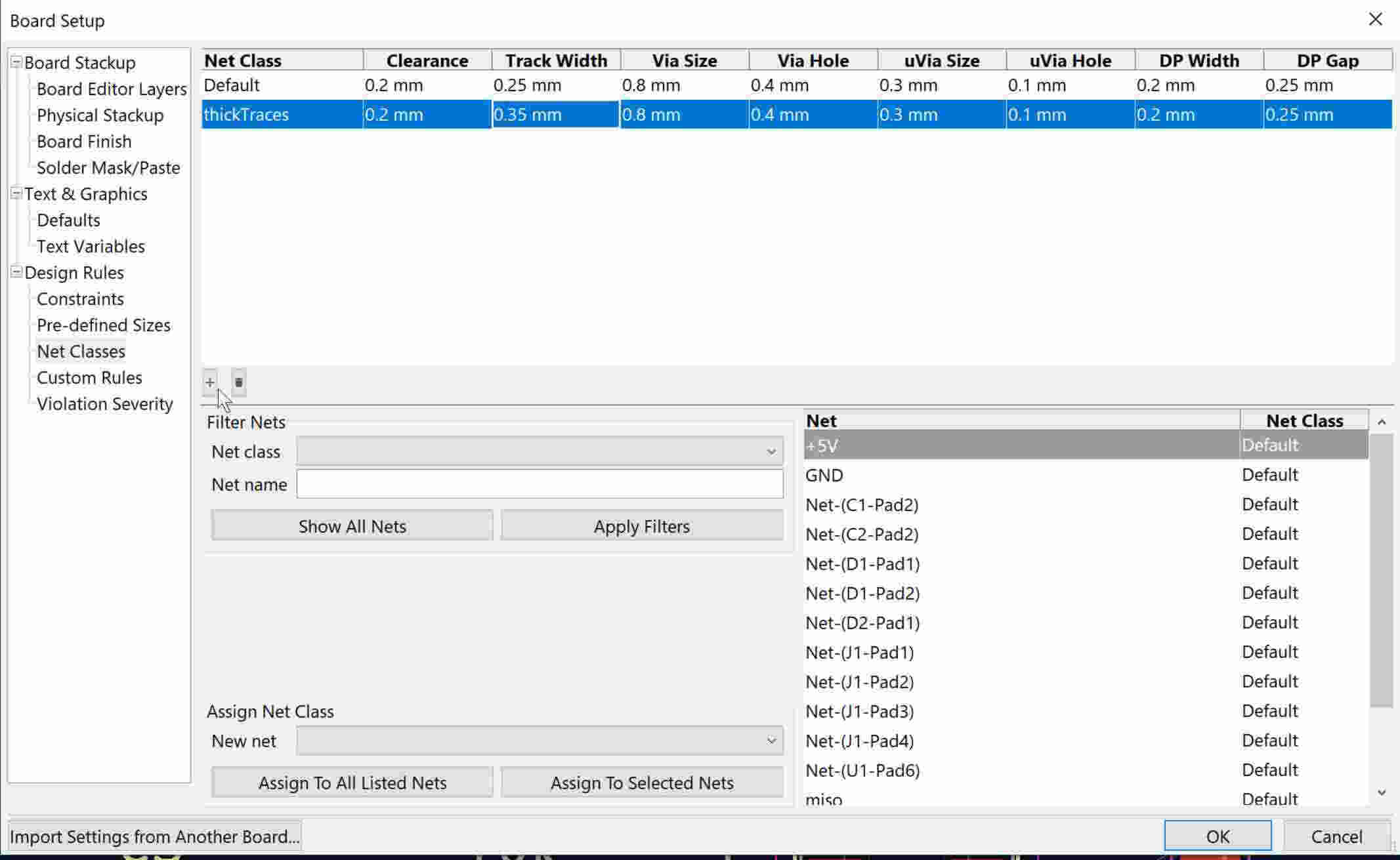
I also added a pre-defined track width with a thicker trace.
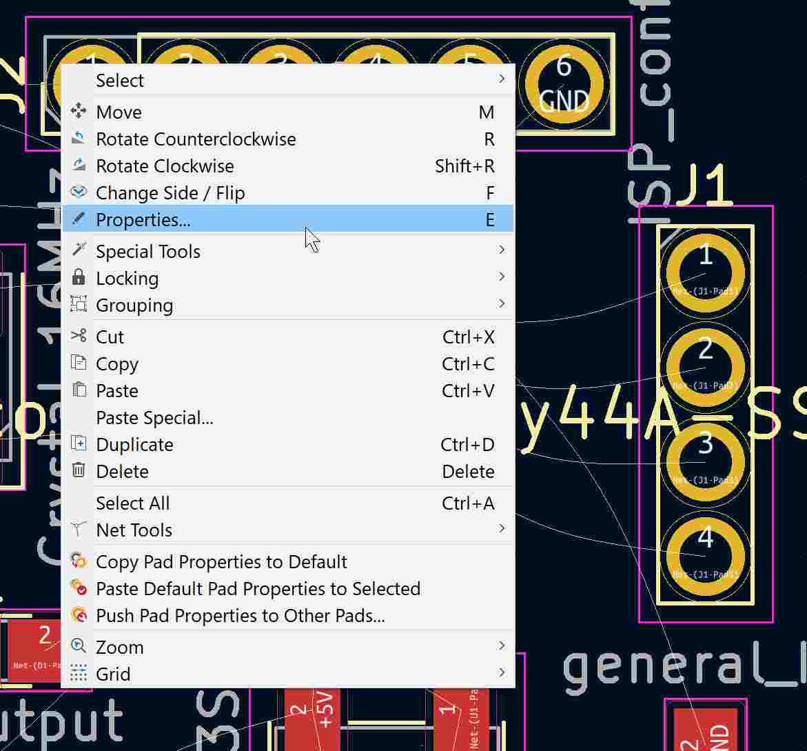
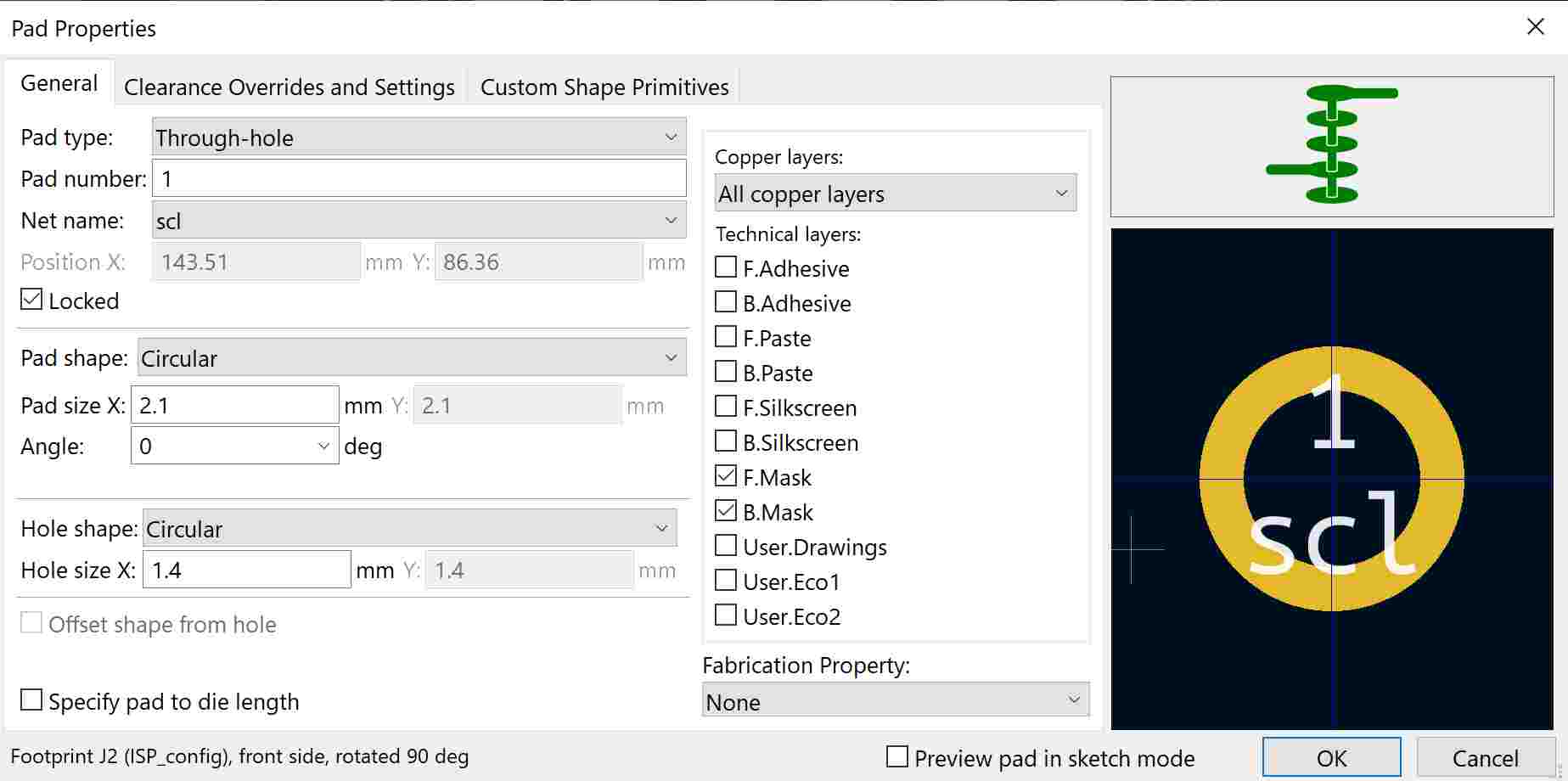
Then I wanted to edit the shape of the pin header pads since our local instructor recommended us to use oval ones instead of the standard circular ones because they are easier and better to solder components to. So I right-clicked a pad and went to Properties....
There I changed the following settings and clicked OK.
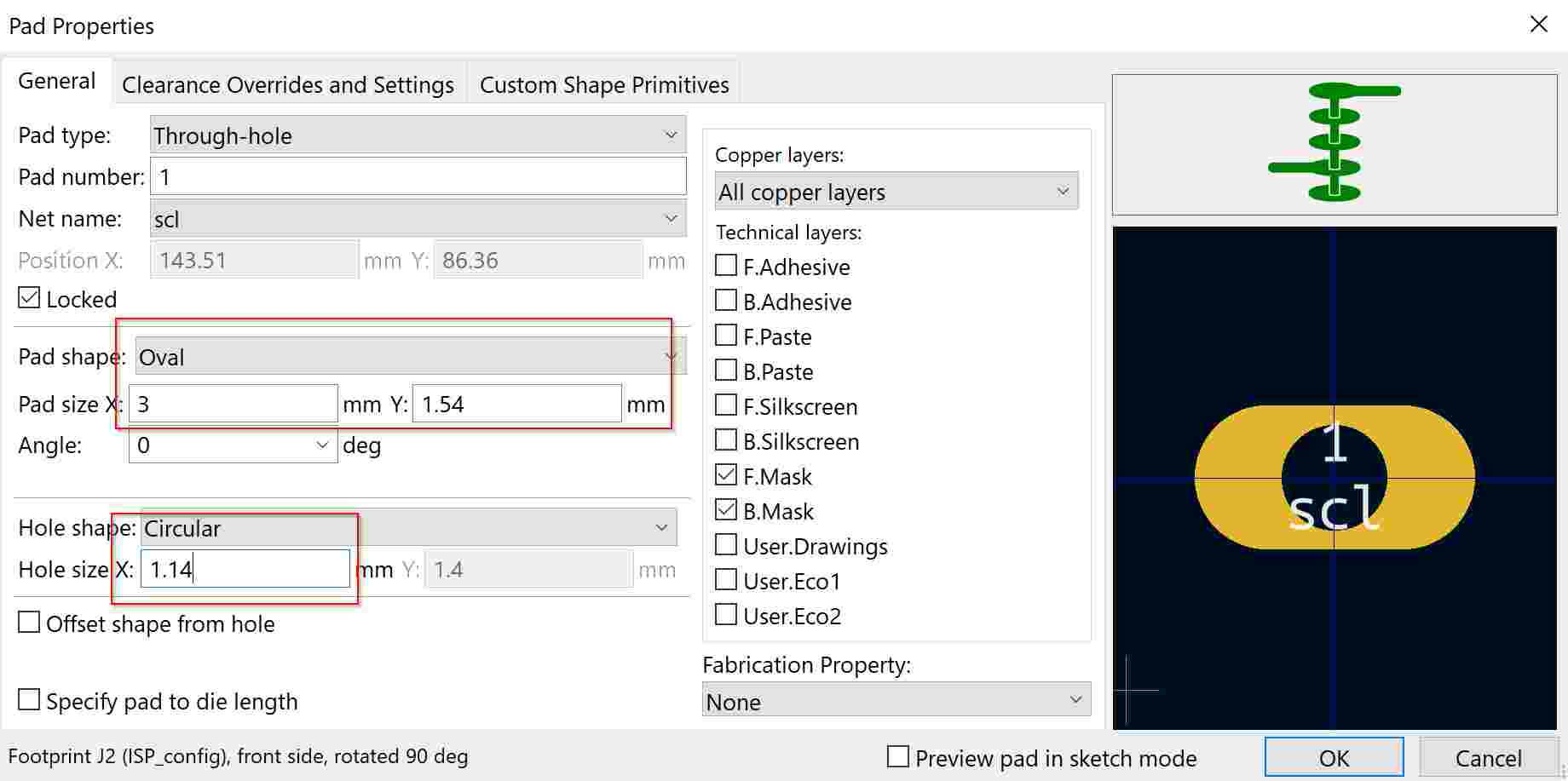
I then right-clicked the edited pad and chose Push Pad Properties to Other Pads....
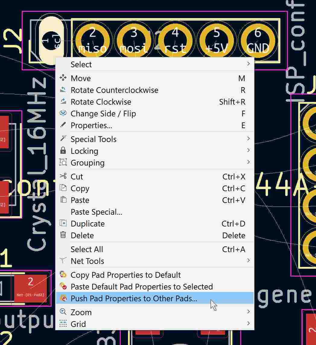
And unchecked all options.
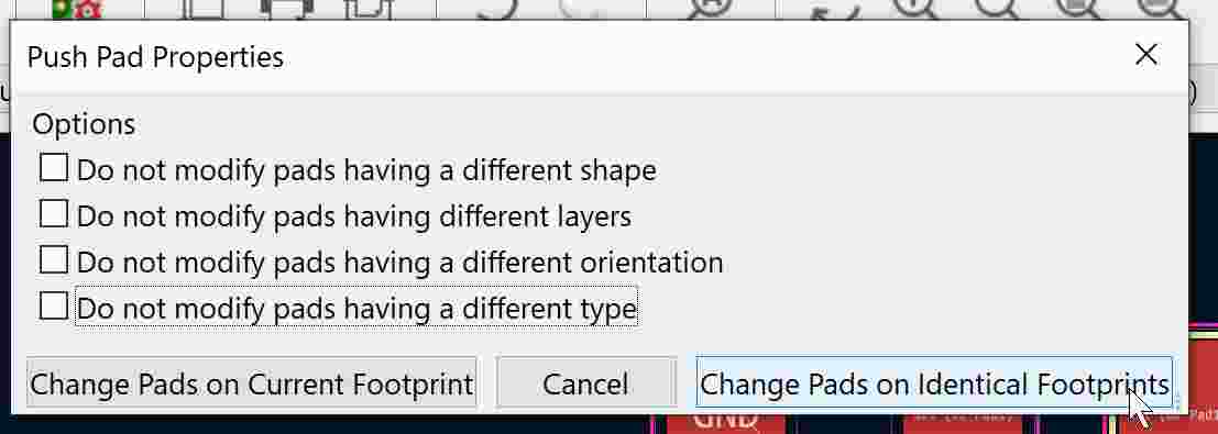
I then did the same to the other pin header block.
The next step was then to make all necessary connections to the 5V power port.
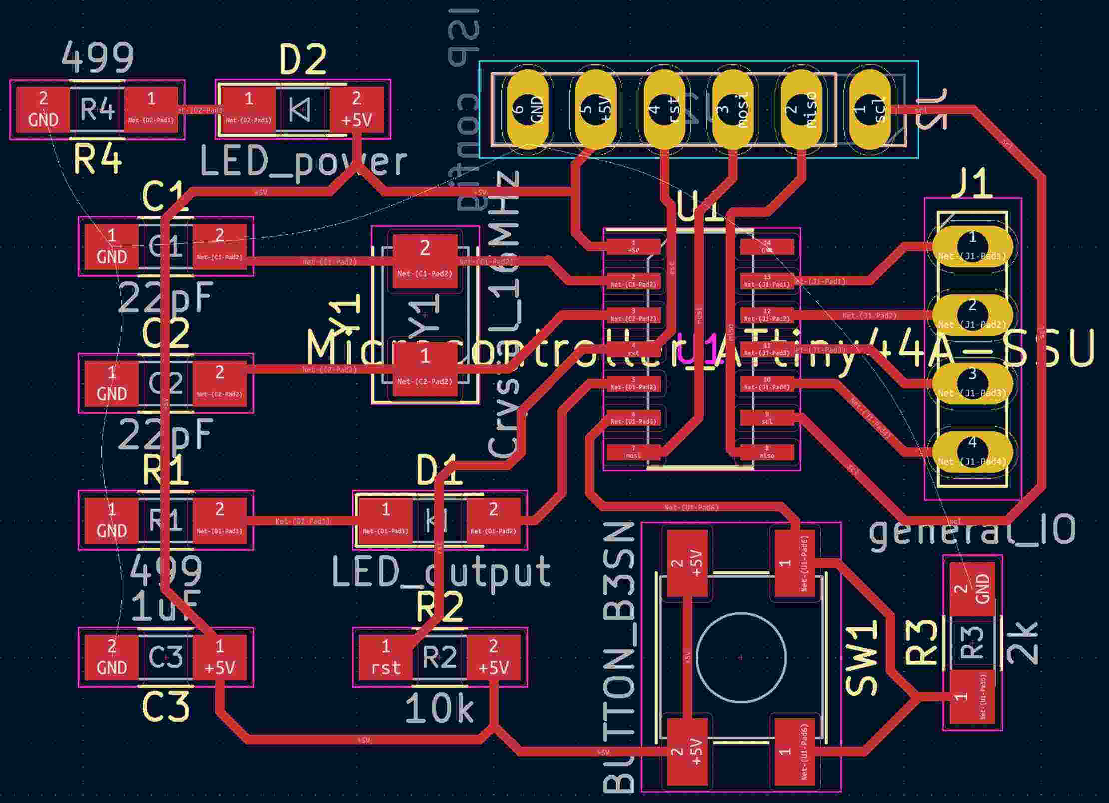
And for the last step, I added a ground layer instead of individually connecting the ground pins to the ground port. To do that, I added a filled zone.
Selected the ground copper layer.
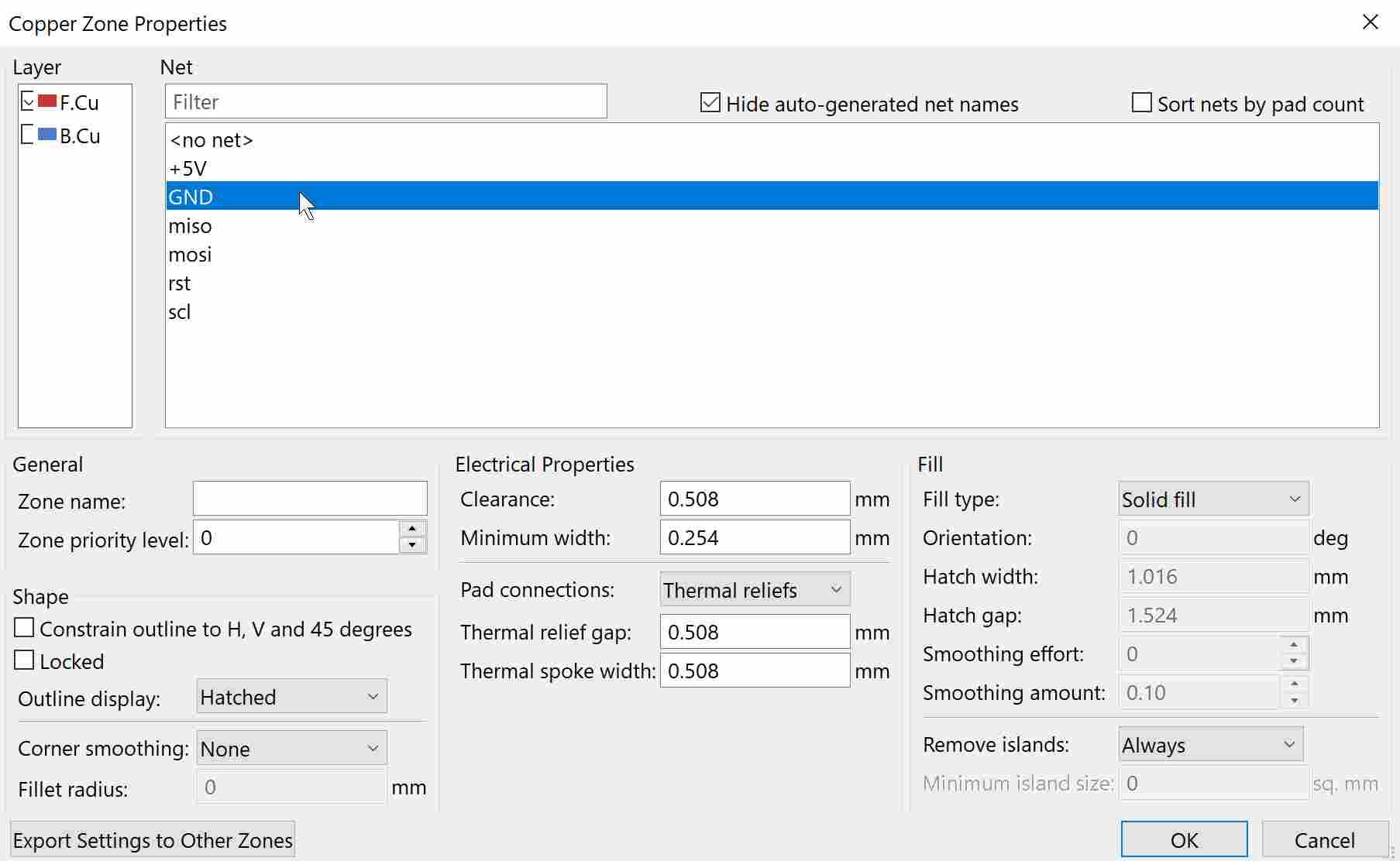
And drew a box around the connected components.
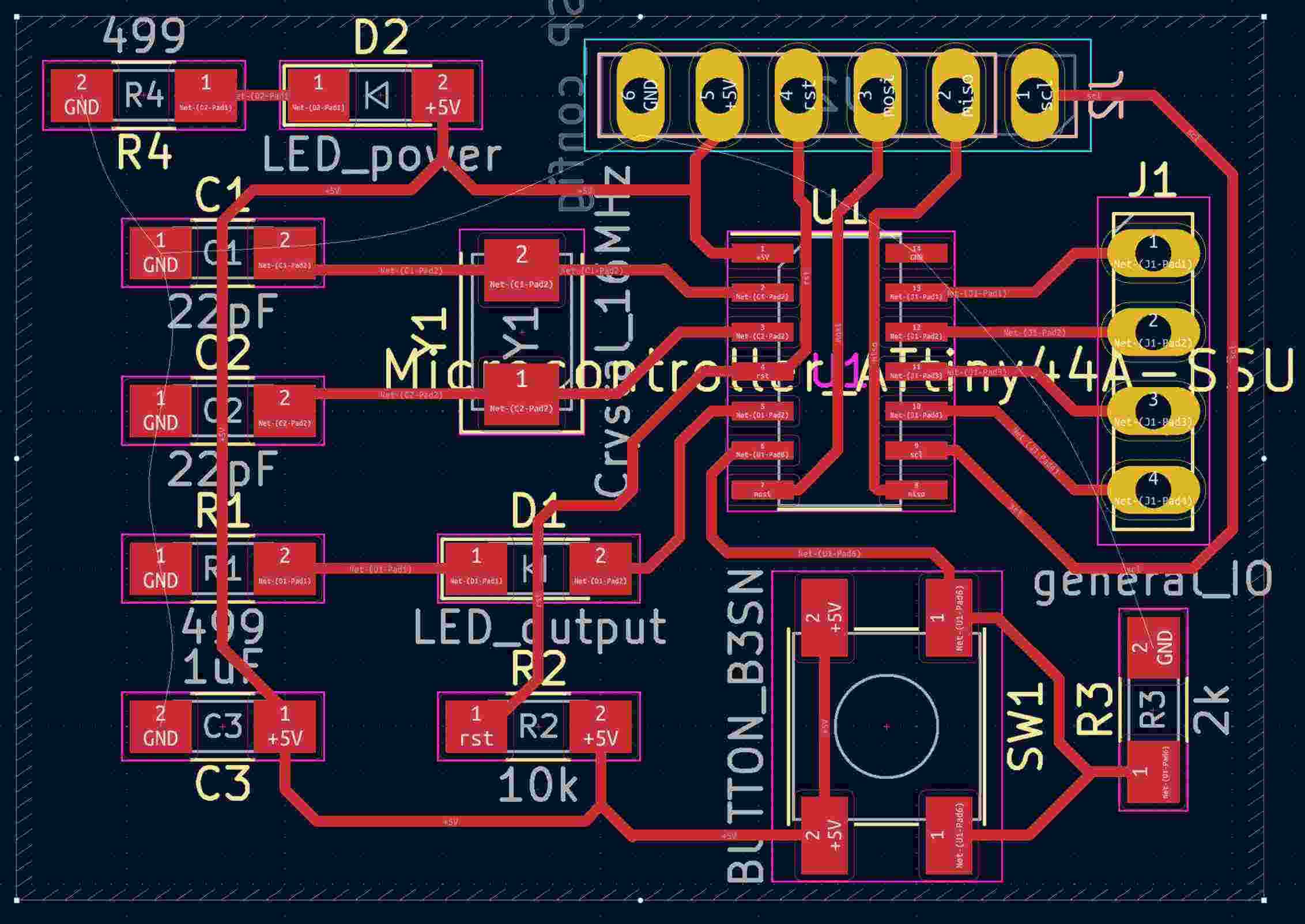
To show that layer, I pressed the keyboard shortcut B, and made sure all ground islands are connected to each other.
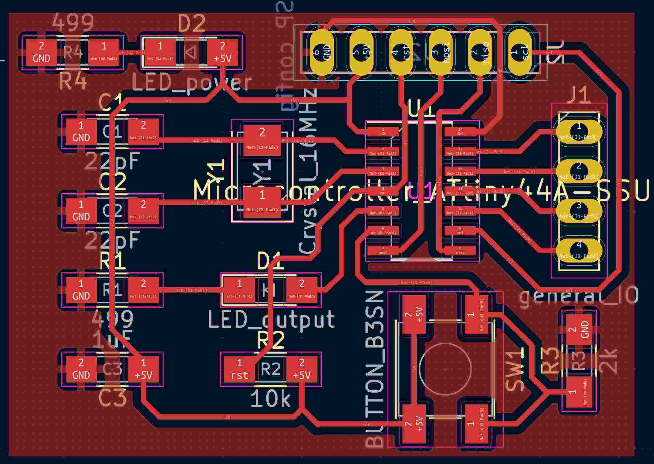
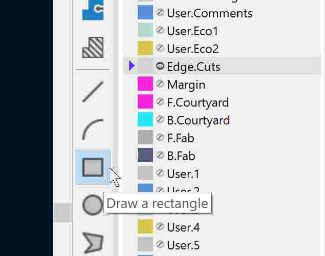
I then activated the Edge.Cuts layer and drew a rectangle around the ground layer.
Last check for missing and/or invalid connections.
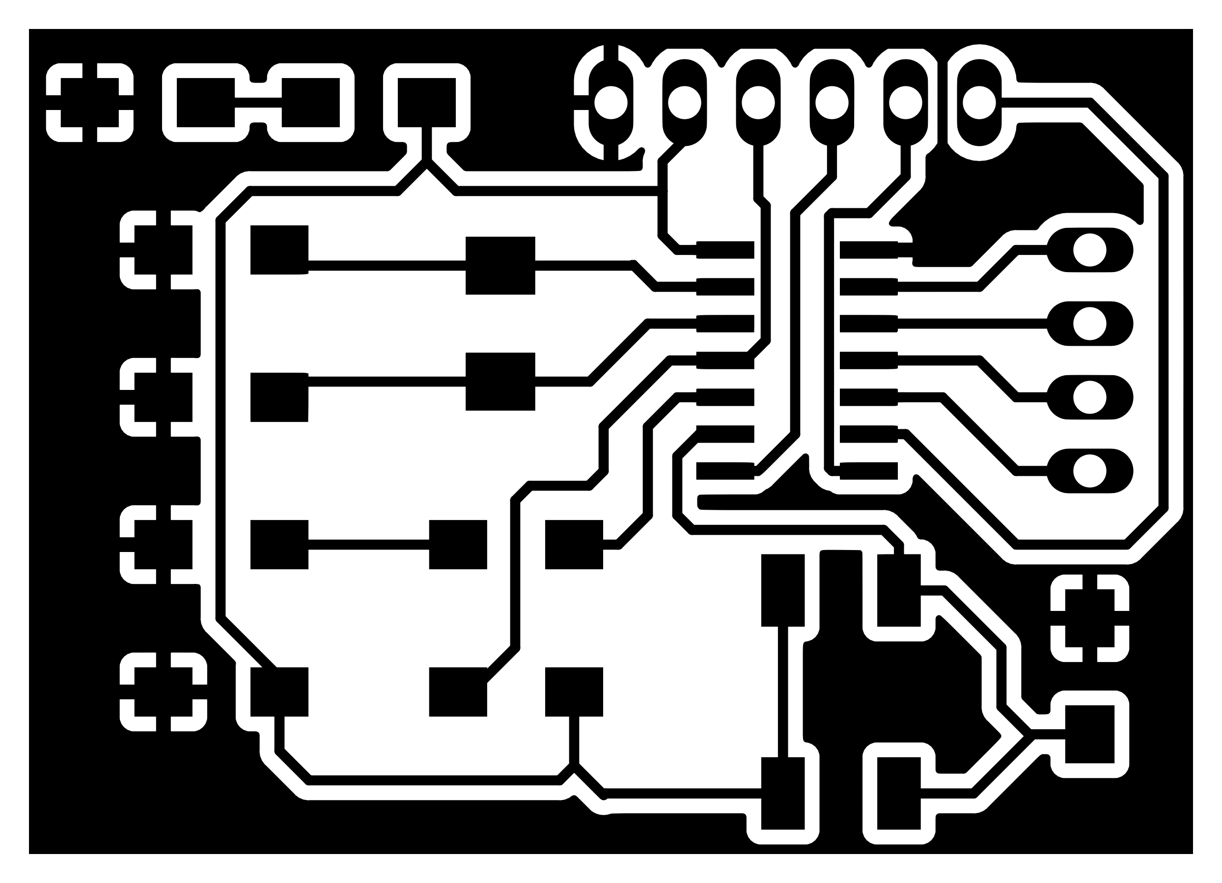
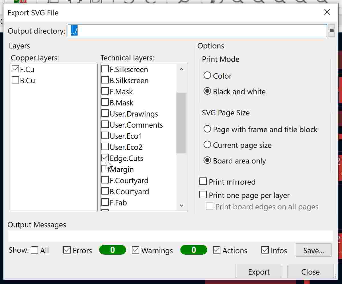
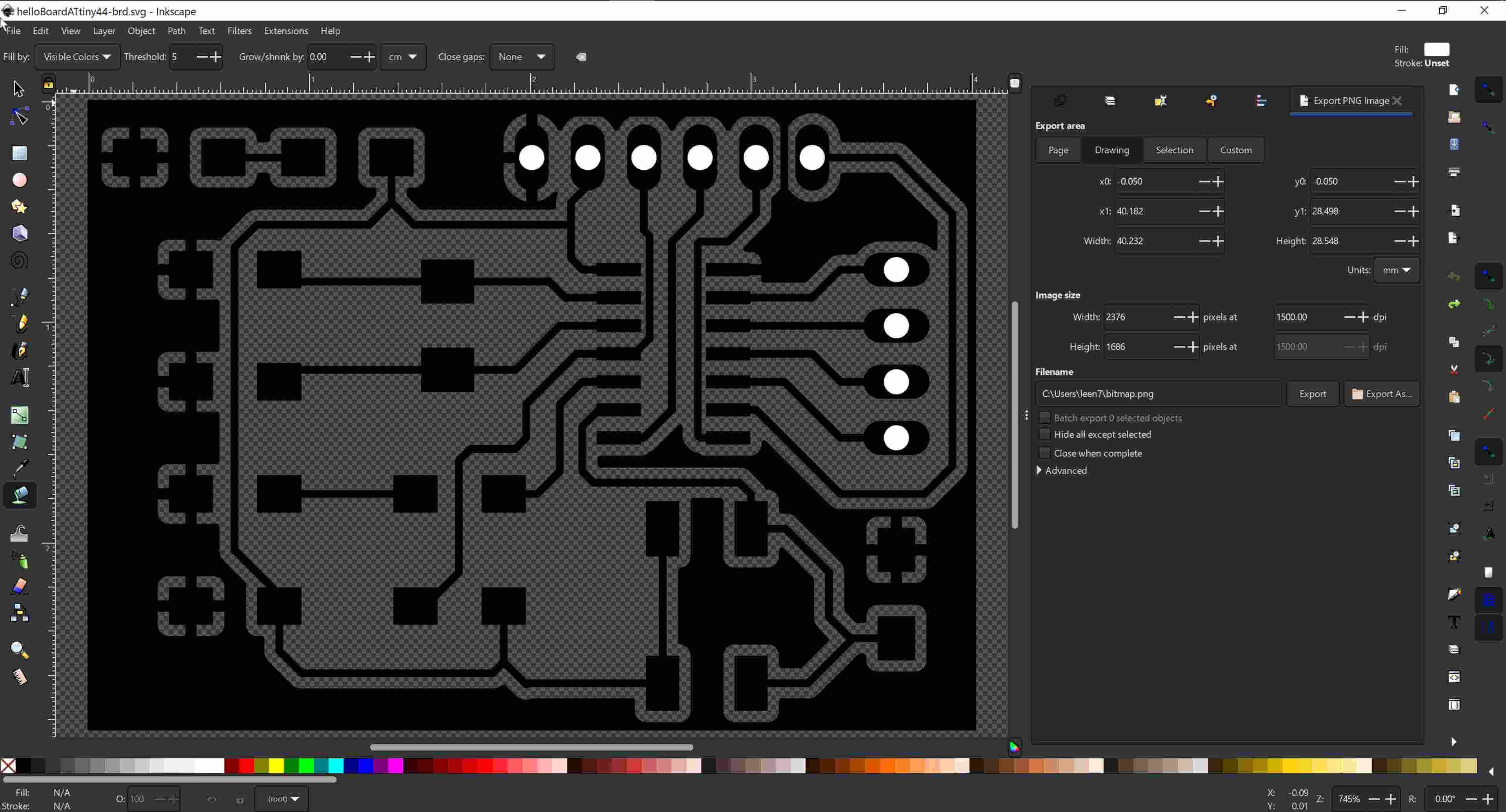
Satisfied with the result, I exported the board design as an SVG file.
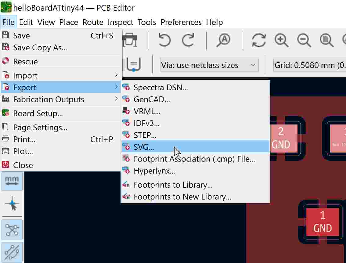
Here, I made sure to select F.Cu and Edge.Cuts, Black and White, and Board area only.
I then opened my file in Inkscape and filled the transparent layer with white.
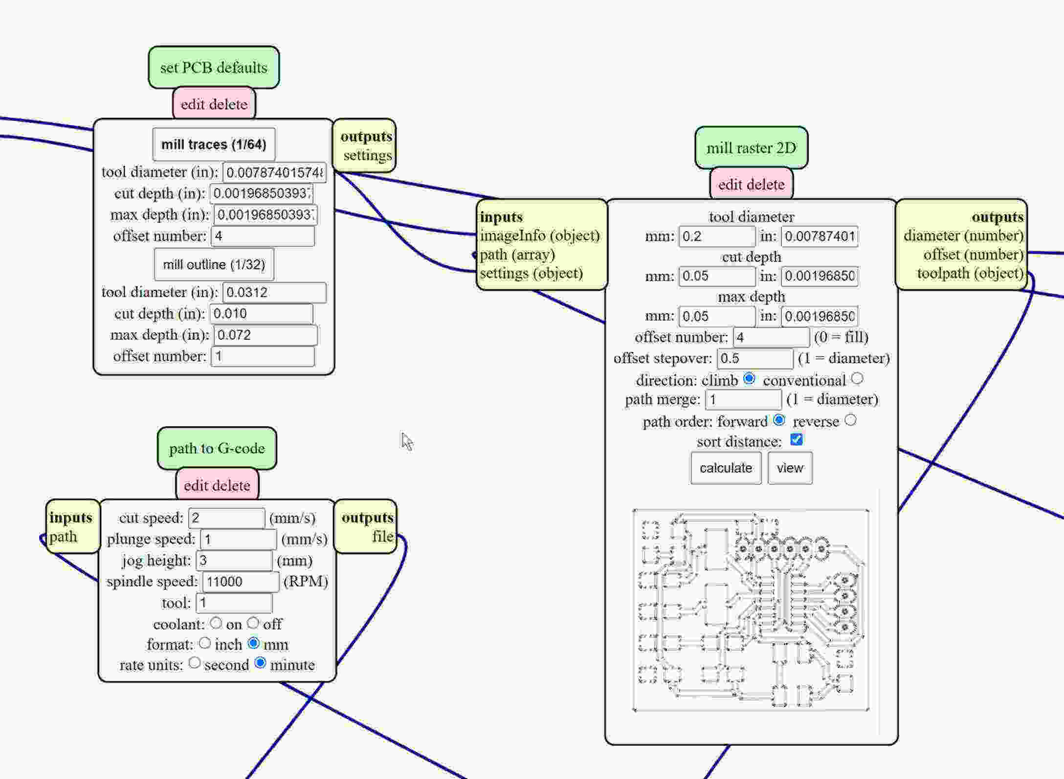
Knowing that our local instructor has problems with running mods PCB milling with SVG files, I did a quick test whether I would be able to create a gCode from my file.
As it turned out, mods> had problems with the image file.
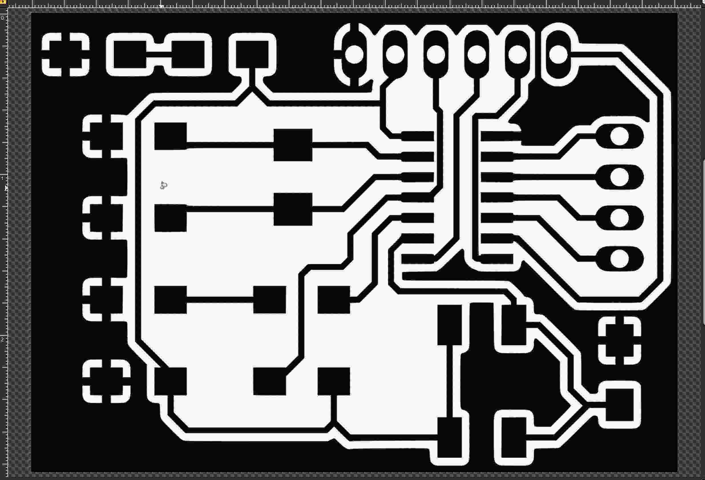
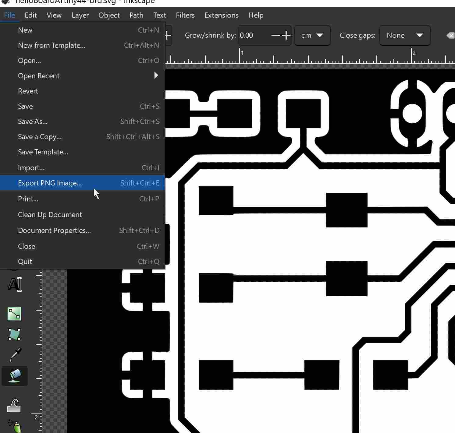
So I went back to Inkscape and exported my milling files as PNG images.
Problem
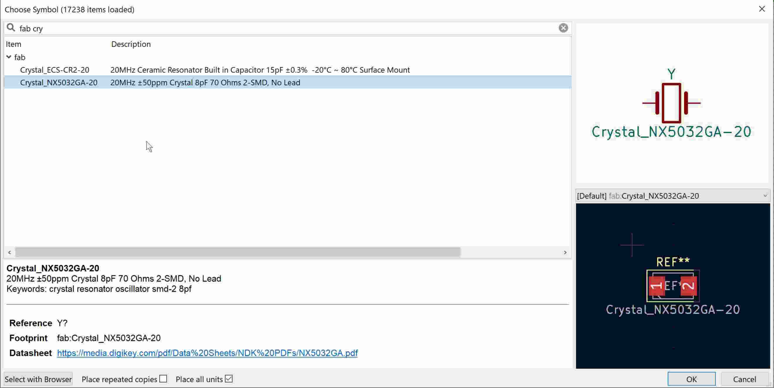
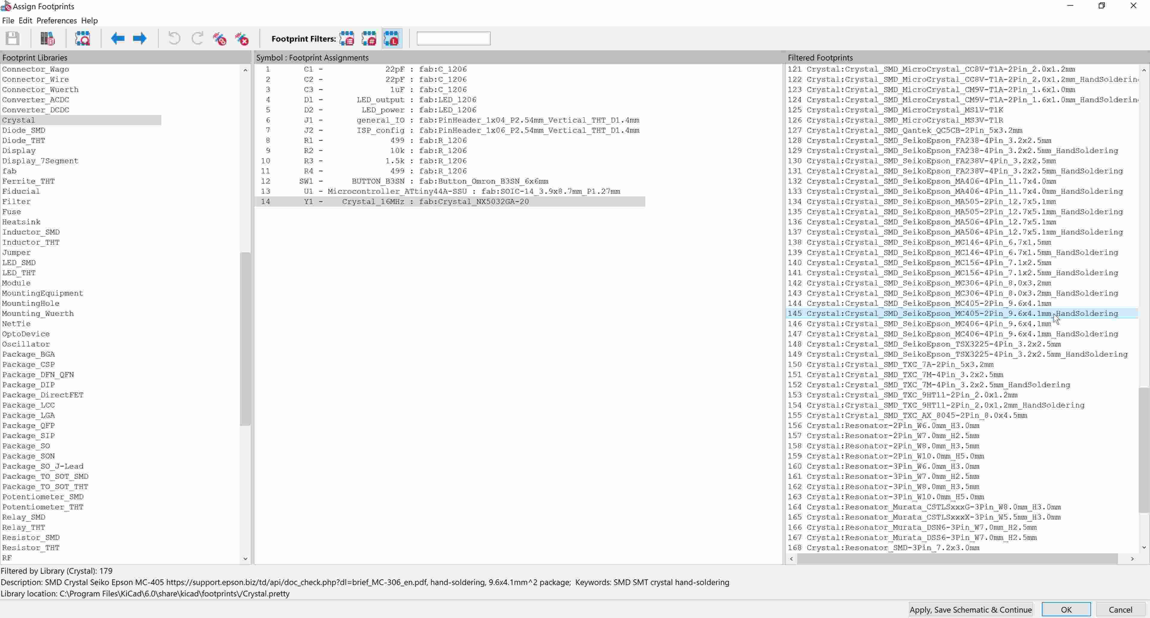
Went I went to the Fablab to mill the board, I discovered that the ordered crystals had not arrived yet, so I had to use a bigger size SMD crystal package. So I went back to KiCAD but could not find a matching footprint for the crystal we had, so I had to choose the closest one. I did that within the Footprint Editor.
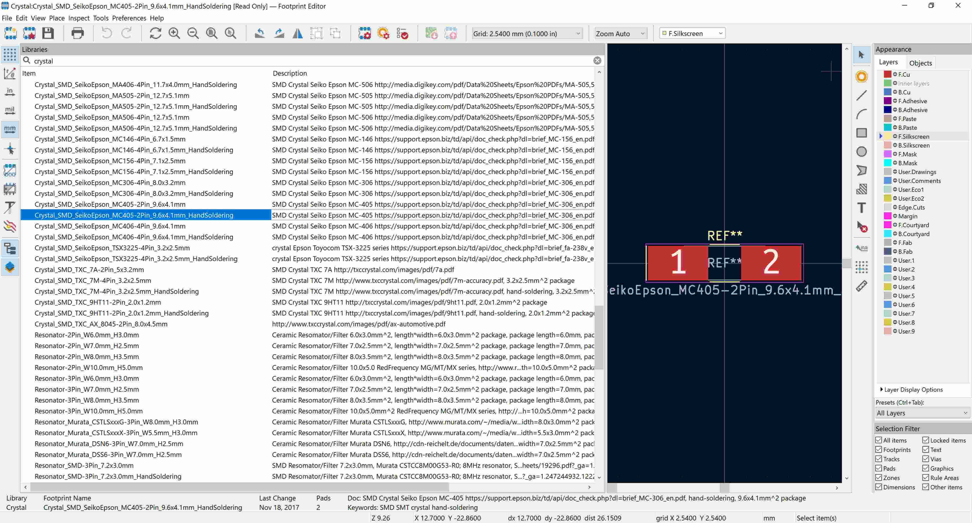
And then had to change the assigned footprint to the one I found.
I then went back to the PCB editor and updated the components.
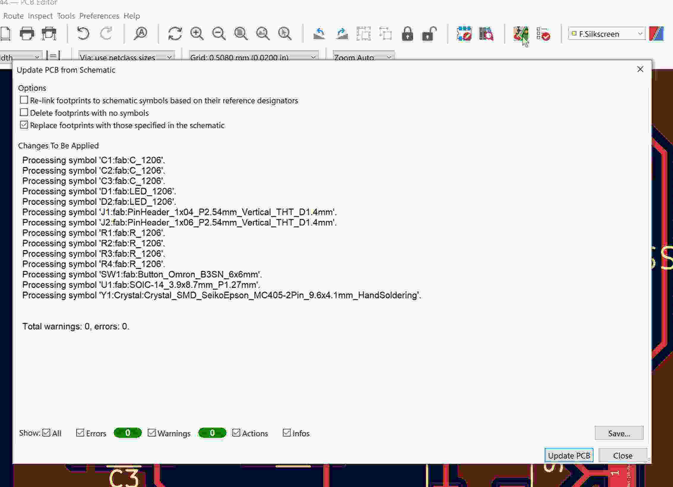
But that change messed up my carefully thought-through design, so I had to go back to the drawing board again.
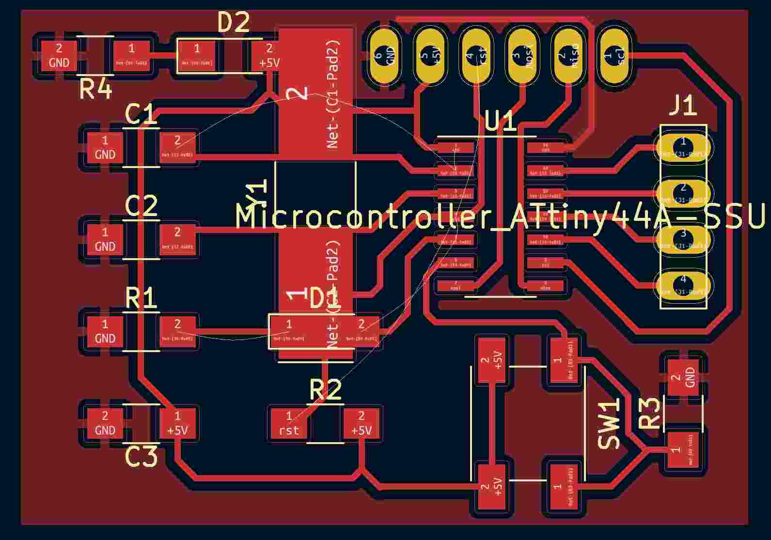
The first thing I did was to edit the footprint manually using the Footprint Editor to make the pads smaller and place them closer to each other, since this footprint is a bit too large for the crystal package we have.
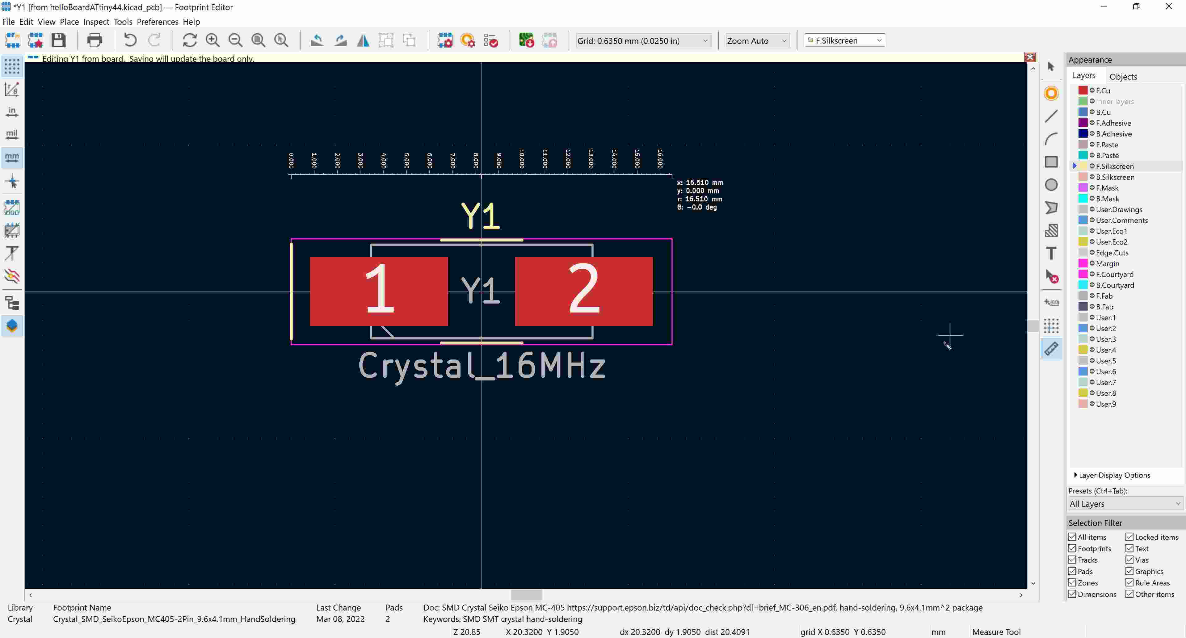
I looks a bit better now, but I still had to redo my wiring and placements :/.
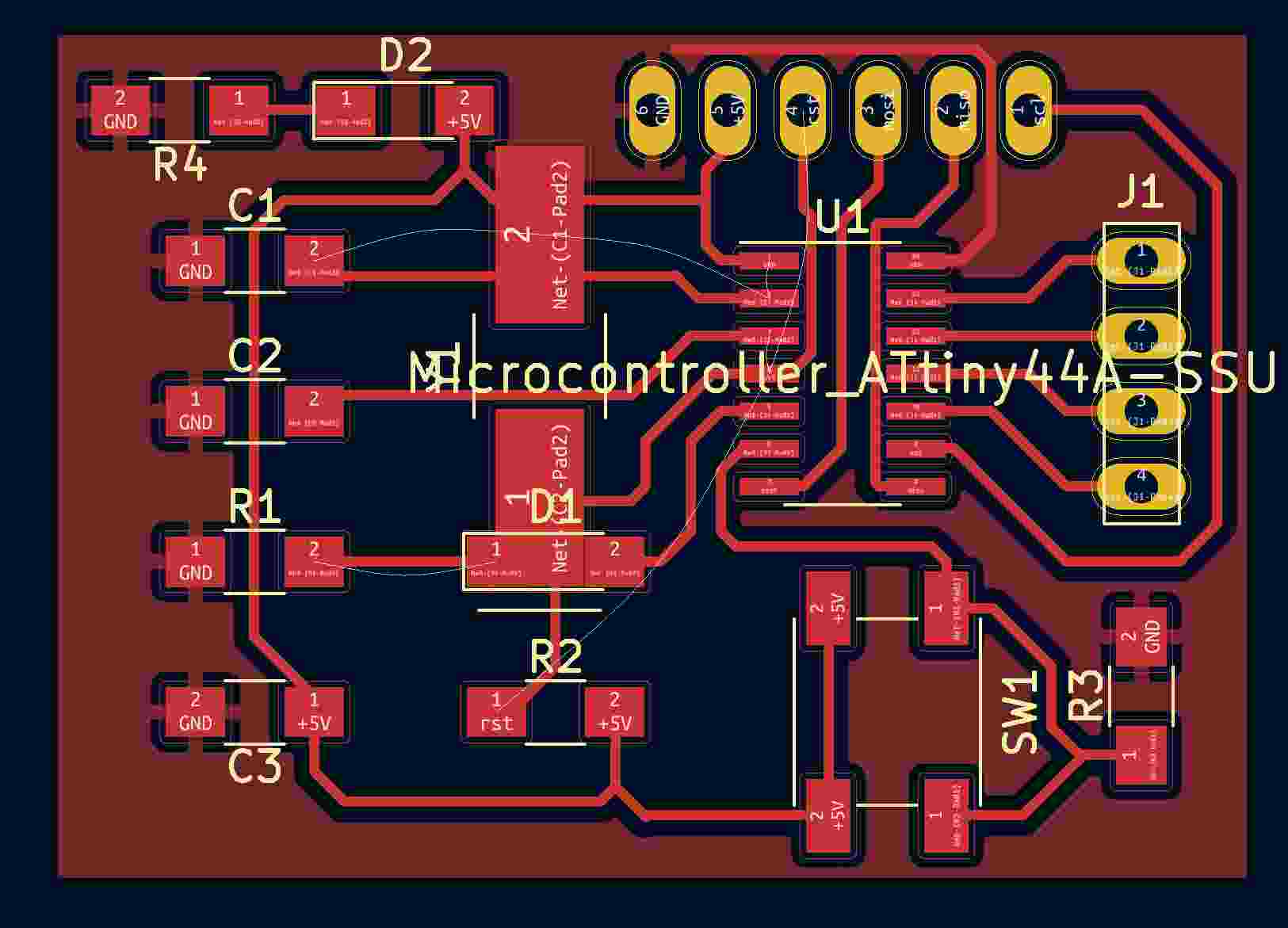
So I ended up placing it like this, since according to our local instructor we should always place the crystal as close as possible to the microcontroller.
I then re-added the ground layer for my final step.
Only to run into another problem: my ground pin is isolated now.
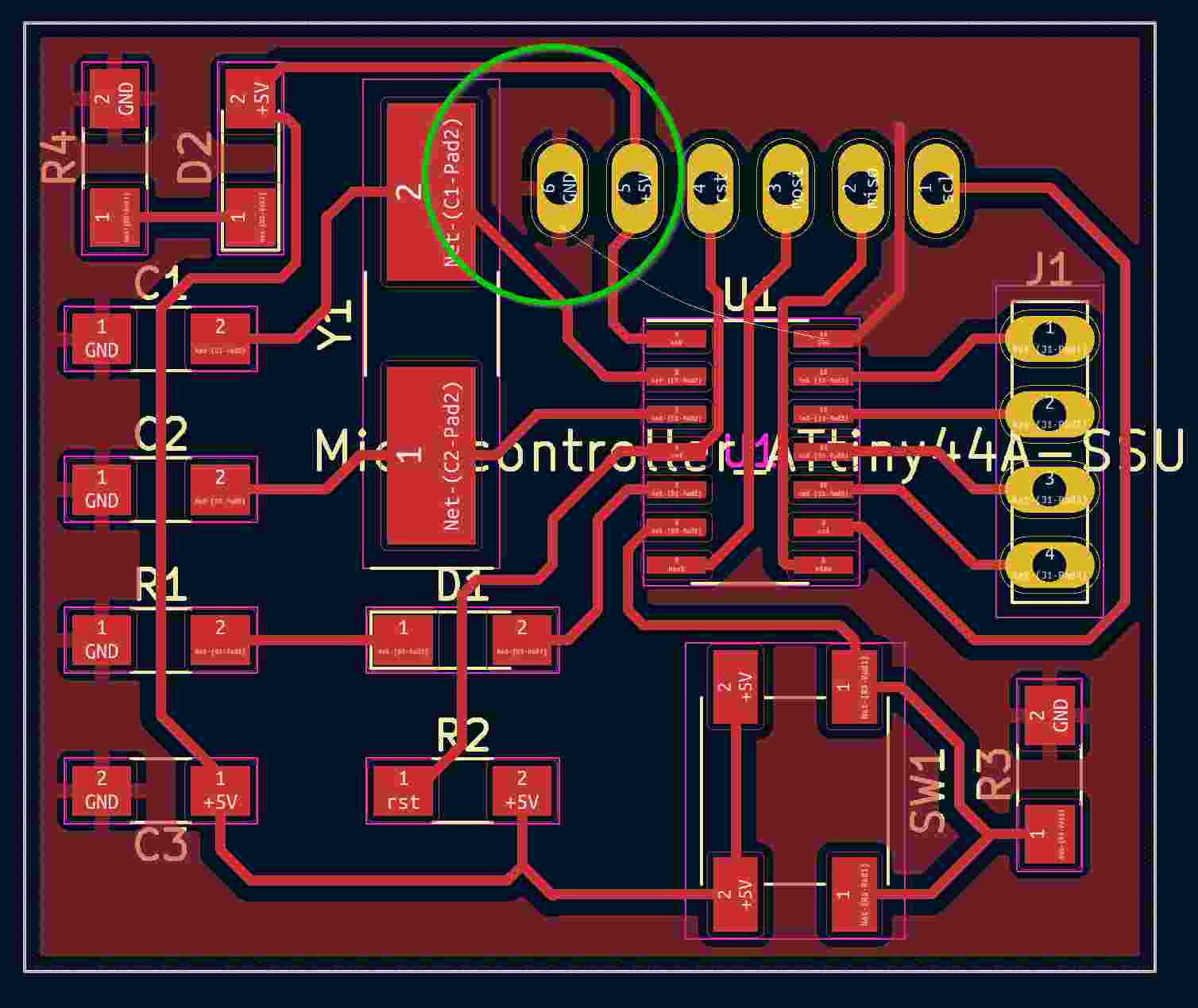
Running out of options of how to solve this problem without having to redesign the whole board, I decided to add a zero-ohm resistor to bridge the two ground island.
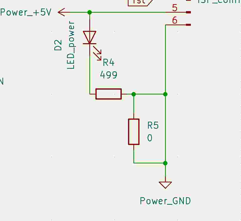
This way, although the software does not realize that this new resistor functions like a wire, it should solve the disconnection problem when I solder it there.
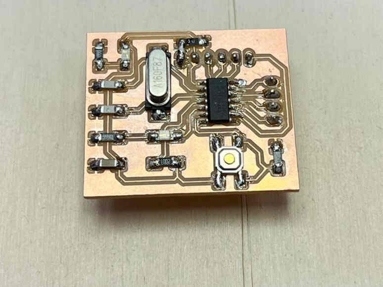
Milling the PCB
After editing the board, I went through the export and conversion to PNG and prepared my milling files.
Milled Hello-World Board
.jpg)
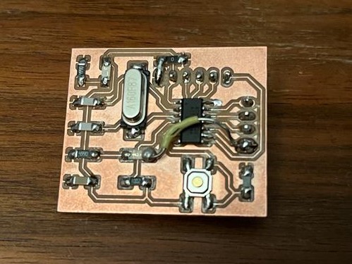
Stuffed Hello-World Board
Testing Hello-World Board ATtiny44
For testing my board, you can check what I've done in Assignment 9. There, I had to fix a connection between the microcontroller and the LED before I was able to run my blinking test code.
And then I uploaded this simple code:
/*
Blink

Turns an LED on for one second, then off for one second, repeatedly.

Modified from the code found in:

https://www.arduino.cc/en/Tutorial/BuiltInExamples/Blink
*/

#define LED PA3    // ATtiny44 pin 10 that is connected to the on-board LED

// the setup function runs once when you press reset or power the board
void setup() {
	// initialize digital pin LED as an output.

	pinMode(LED, OUTPUT);
}

// the loop function runs over and over again forever
void loop() {
	digitalWrite(LED, HIGH);   // turn the LED on (HIGH is the voltage level)
	delay(1000);                       // wait for a second
	digitalWrite(LED, LOW);    // turn the LED off by making the voltage LOW
	delay(1000);                       // wait for a second

}
And here is my hello board ATtiny44 blinking!