5. Electronics Production
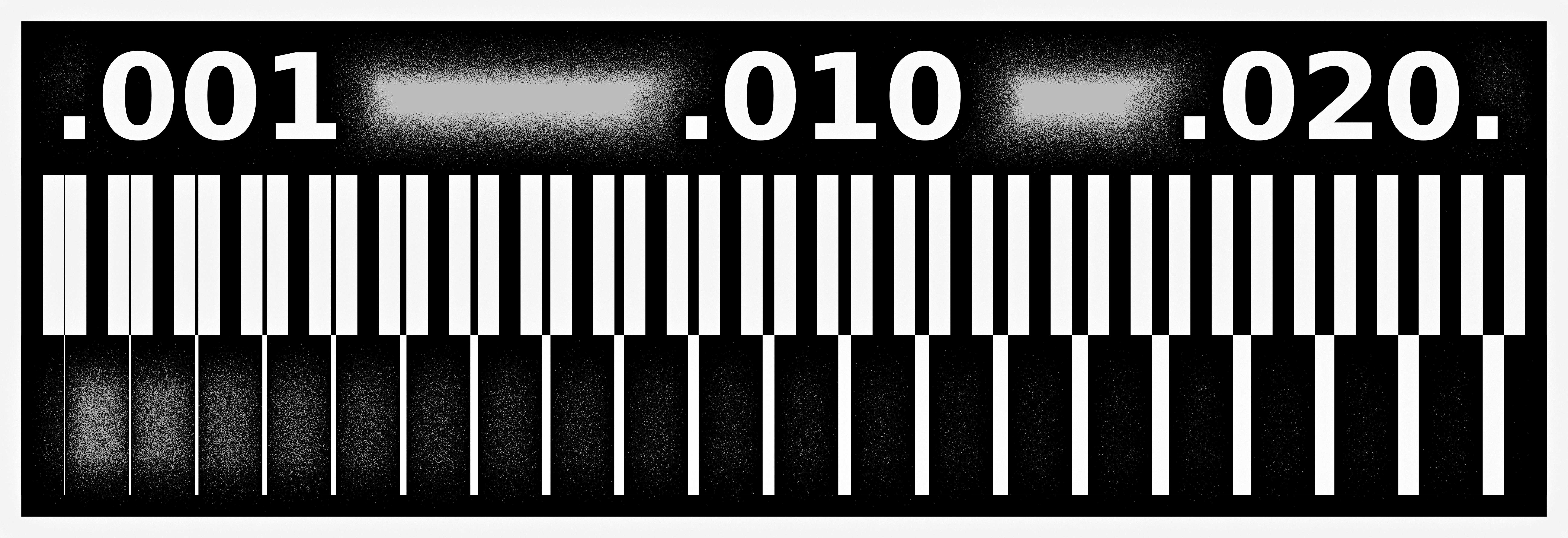 Figure 1. Milling Line Test.
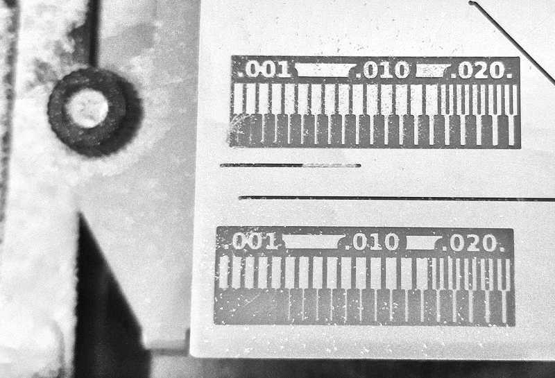 Figure 2. Climb and Conventional Milling Test.
5.1 The production of an in-house PCB
5.1.1 Milling
PCB milling is the non-chemical procedure where copper portions of a PCB plate are physically removed with a CNC precision milling machine for the creation of an electronic circuit board.
5.1.1.1 Materials
- Precision CNC machine Roland monoFab SRM -20
- Allen key
- double-sided tape
- PCB plates (copper & paper based — PCB thickness 1.55mm | Universal thickness is 1.70mm) FR1
- 1/64 inch end mill bit (for the inner cut)
- 1/32 inch end mill bit (for the outer cut)
- brush to remove dust from the plates and the machine
- japanese cutter knife
- metal spatula for removing the plate from the base
- laptop with access to V-panel software to communicate with the CNC machine
- access to Mods or Fa-Modus to generate the files
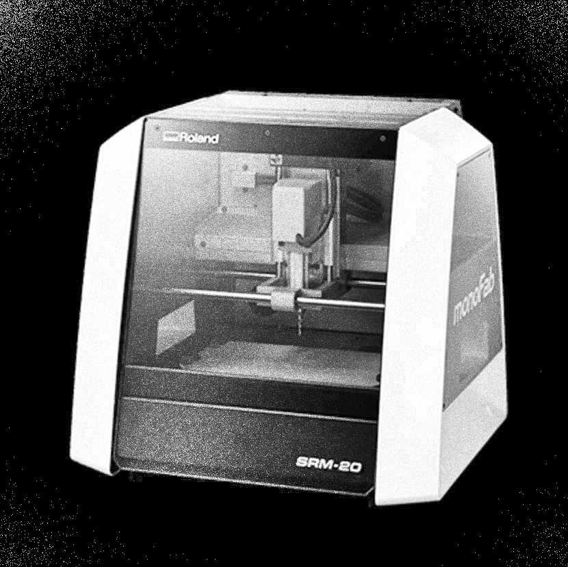 Figure 3. Roland SRM-20.
5.1.1.2 Procedure
a. Prepare the desired files.
Hello D11C - Traces / Outline
Serial UPDI - Traces / Outline
The PCB’s diagram is produced firstly on “KiCad” as .SVG file, and is secondly used as matrix for the creation of a negative version of the layout on “Inkscape”.
The file is exported as .PNG using 1000 dpi to ensure correct size and proportions and the preparation of the script is done in “Mods CVA Community Edition”.
The SOP is as follows: 1. Select programs > open program and choose the device (Roland SRM-20 mill Absolute) or 1. Select Programs > Open Program > connect > Roland SRM-20 PCB 2. Set PCB values (mill size, speed, jog height and traces (1/64 inch end mill)/outline (1/32 inch end mill).
5.1.1.2.1 Milling process
a. Prepare components
b. Turn on the CNC machine
c. Fix the PCB
With clean hands stick a stripe of double tape around the edges of the PCB plate, refraining from overlapping it. Remove protection cover and press against the sacrifice board. Avoid contact with the copper plate at all times by using a piece of paper or cloth to press down.
d. Load the end mill
Important: End mills are delicate, therefore they must be handled with care. An allen key is used to loosen and tighten the collet. The end mill (1/64 inch) should be introduced and held in place during the tightening of the collet.
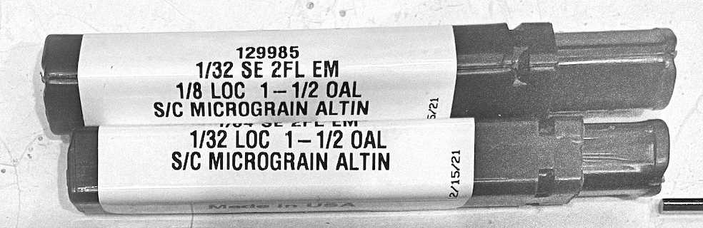 Figure 4. Two samples of the 1.32 inch end mill used for the outline milling.
e. Set “X”, “Y” & “Z”
“X” & “Y” are positioned on the PCB plate with the use of the V-panel. “Z” is done independently. The V-panel is equipped with the possibility to set the cursor at different speeds (Continue, x100, x10 and x1), enabling an accurate and safe procedure. The end mill should be placed approximately 3 millimetres above the PCB plate and the collet opened for its release, while it is being held and let down gradually until it touches the plate slightly. At this point, it is ready for the final tightening.
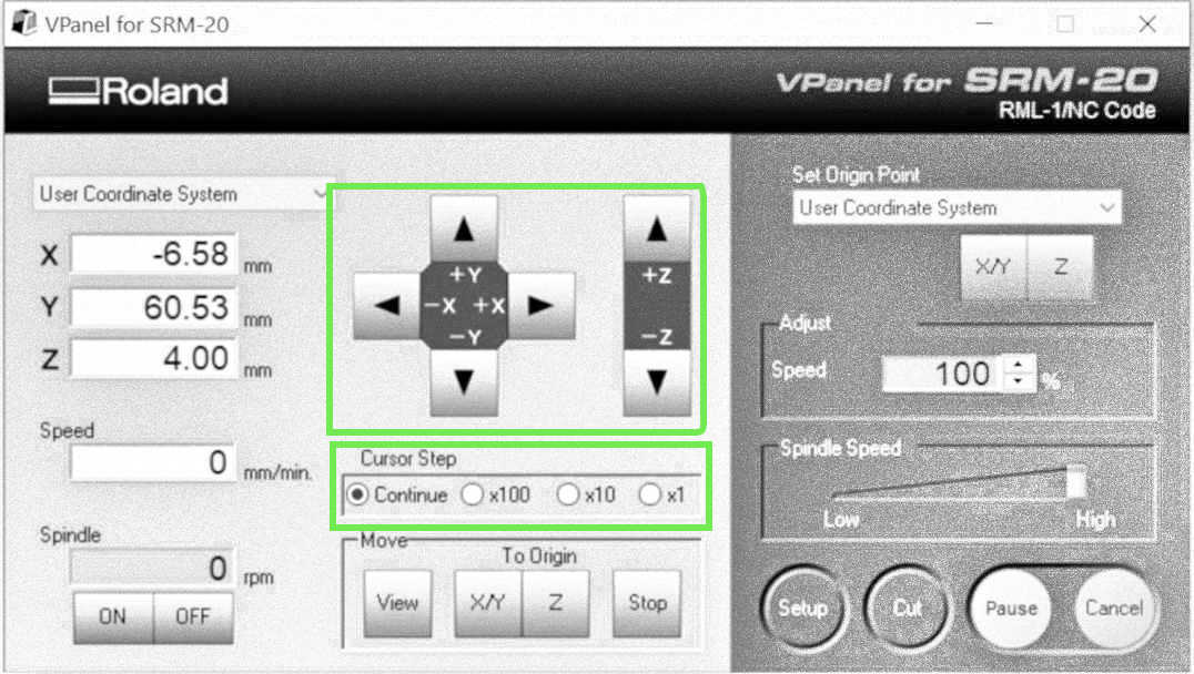 Figure 5. VPanel Settings.
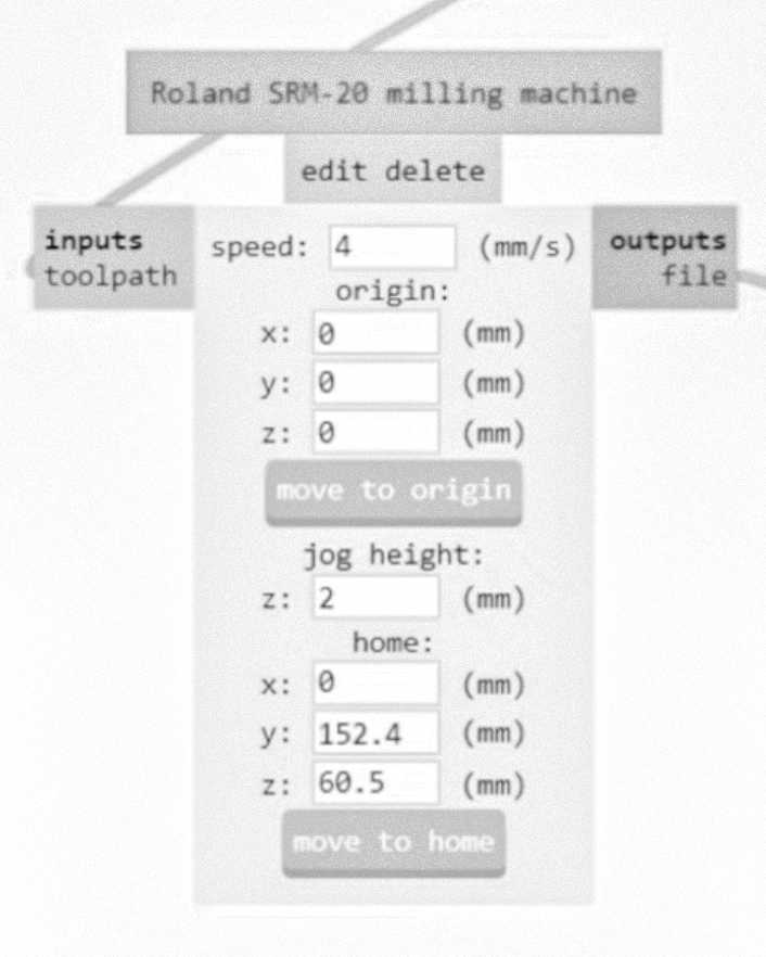 Figure 6. “Mods CVA Community Edition” settings for the interior section of PCB milling.
g. Change of the end mill (1/32 inch) to produce the outline
h. Set “Z” again
i. Cut-out the design and remove finished PCB from CNC machine
5.1.2 Soldering
With a freshly produced PCB in hand, it is time to solder the electronic components.
Soldering is a crafty endeavor that requires repetition in order to achieve the sufficient so-called “muscle memory”. It proves important not to be discouraged by beginner’s unsatisfactory results. Soldering is a trial an error procedure. The best results come with practice as technique varies from person to person, materials, settings, components, tools and support available.
5.1.2.1 Materials
Aside of the list of tools and gadgets (see below); a PCB board and electronic components are also a necessity.
General list of basic tools & materials to have at a soldiering station:
-
Multimeter
-
Soldering iron w/stand (Yihus 8786F I 2 in 1) @ 398ºC
-
Soldering wire (L-9317/0,5)
-
Lamp
-
Tweezers
-
Copper fiber
-
Vacuuming Wire or De-soldering Braid (3S-Wick) size AB(3)
-
Copper pliers
-
Soldering Flux
Optional
-
Wet sponge
-
Magnifying glass
-
Watchmaker’s Magnifier
-
Solder Sucker
-
Milled PCB
5.1.2.2 Procedure
Firstly, create a ‘shopping list’ to efficiently gather the necessary components for the board. Getting acquainted with electronic components takes time, meaning that at first, most electronic parts will tend to look too similar. Therefore, it is highly recommended placing a piece of double-sided tape next to each component’s names, in order to keep clear reference between name and/or description and shape.
Please note the error in the image below:
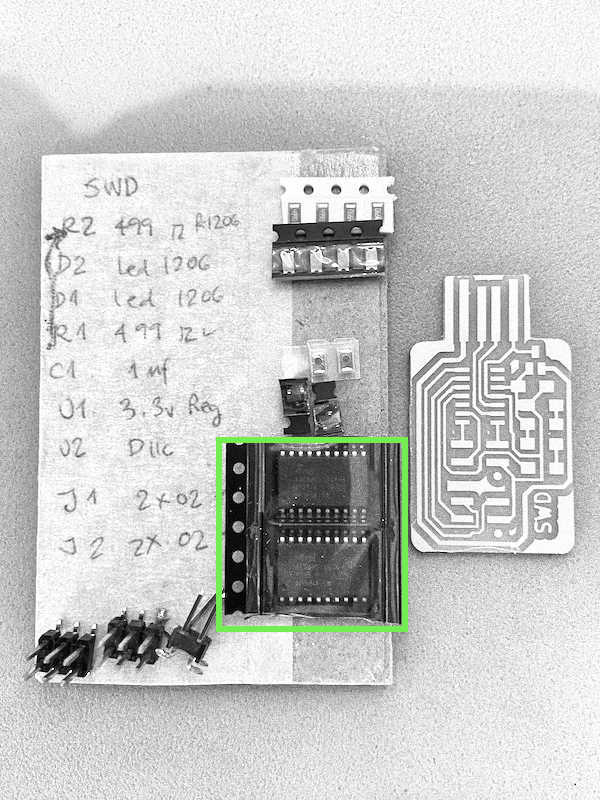 Figure 7. SWD PCB ‘shopping list’.
The SAM D11C (Micro Controllers AVR (AT), arm (ATM) and ESPRESSIF (ESP))required for the SWD board being mistaken [by me] for a SAM D 21E. This deviation was simple one to notice and fix by having all components laid out as suggested above. The correct part was easily substituted and the wrong one returned to its drawer for future use.
Secondly, preheat soldering iron to about 400 Cal, making sure the tip is in good condition, firm and clean. Potency should be between 15w and 30w, to keep from damaging the components. What tends to work best is to start by heating up the connection in question and not the solder. Then, apply the solder. The solder usually runs towards heated elements, therefore is important to follow this procedure along the way.
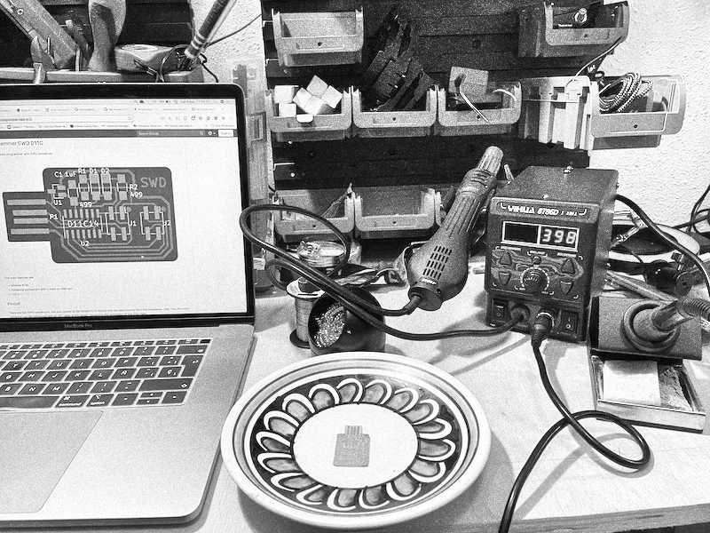 Figure 8. SWD PCB soldering procedure.
5.1.3 De-bugging
Once the components are soldered, connectivity needs to be revised with a multimeter to make sure everything is working.
5.1.3.1 Materials
The list of materials required for de-bugging is the same as for soldering.
5.1.3.2 Procedure
The multimeter needs to be on check mode with sound. Place a wand on each side of a trace between two components. Sound means connection. If that connection is undesired, check for excess solder. If no connection, re-flow solder in the intended connection.
5.1.3.2.1 Top Down Debugging Procedure
Figure 9. This section is a deeper dive into the aformentioned subject and is meant to serve as a page marker — [mainly] for personal use.
5.1.4 Programing and edbg Atmel Embedded Debugger
The milled and stuffed board needs to be programmed by burning a bootloader into its ATML microcontroller. The procedure is done with the use of a command-line created by Alex Taradov, who offers his code freely, as a gift to the world.
Flashing the board with Mac proved to be impossible, even after many attempts. The solution to such problem was to move to experiment by doing it on a Windows computer. Since I only owned a Mac iOS, my only alternative was to do it by using one the Fab Lab’s powerful machines. In this new setting, the task was simple and straightforward.
 Figure 10. edbg in iOS system.
After not being able to program or sometimes even see my PCBs on my Mac computer, it became relevant for me to take the opportunity and have as an intention to gain a ‘broader operating system experience’ during Fab Academy, meaning I will be attempting to navigate between iOS, Windows and Linux as much as my resources allowed — meaning I would attempt to run them in parallel as much as it would prove possible based on my resources. The actual dream is to proceed with weaning myself from commercially produced technology and slowly move into open source alternatives/ However, change takes time, and I would have to source some “new-used” equipment for the job first.
After about six weeks of setting up the challenge and having programmed the board on Windows repeatedly, I finally sourced a freshly partitioned Windows/Linux computer and went ahead to erase the program one more time, in order to attempt to boot the board once again via the Linux software. The whole process took several hours of work, as well as many trials and error over a few weeks, since navigating from one system to another as a beginner can prove to be a daunting/time-consuming experience. However, I must highlight that, based on personal experience working with the Linux system, I can happily report that this system enables users to dig deeper into the nuts and bolts of computers and programs as no other I have ever used; allowing the user to experiment and learn freely. It was possible to see, from start, that the problems I had been experiencing with my iOS and Windows pieces of equipment were never an issue in this new open-sourced operating system.
5.1.4.1 Materials
-
Computer with edbg installed
-
Already flashed SWD Board
-
SWD Board to be flashed
-
Multiple USB extension cable
-
Raibow cable
5.1.4.2 Procedure
First and foremost, edbg needs to be installed in Linux. To do so, the following commands are to be entered in computer’s terminal:
libudev-dev in Ubuntu sudo apt-get update -y sudo apt-get install -y libudev-dev
Secondly, in order to install edbg, the repository needs to be cloned from GitLab into the computer. With the opened repository as well as the corresponding folder in terminal, the binary files should be run by whilst adding ./file_name each time.
Lastly the programmer is programmed with an already flashed SWD board, by connecting the two (old and new) side by side onto the USB extension cable (plugged to the computer); joined to each other with a little rainbow cable, and by running Taradov’s edbg command-line tool on terminal:
./edbg -ebpv -t samd11 -f free_dap_d11c_mini.bin
5.2 A well functioning board
Although the board doesn’t do much and most of the actual memory inside it’s microcontroller is already consumed by bootloading, it does prove, nevertheless, exciting to be able to gain the basic skills necessary for the use an creation with electronic components.
5.2.1 Example of an operative board
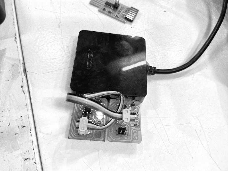 Figure 11. Hero shot of the functioning SWD board.
Resources
- Horowitz, Paul, Winfield Hill, and Ian Robinson. The art of electronics. Vol. 2. Cambridge: Cambridge university press, 1989.