Electronics Design
This week's assignment was to use the testing equipment that was in our lab to test a board then to make a design for a board from an image and then make and program that bord.
Group Testing
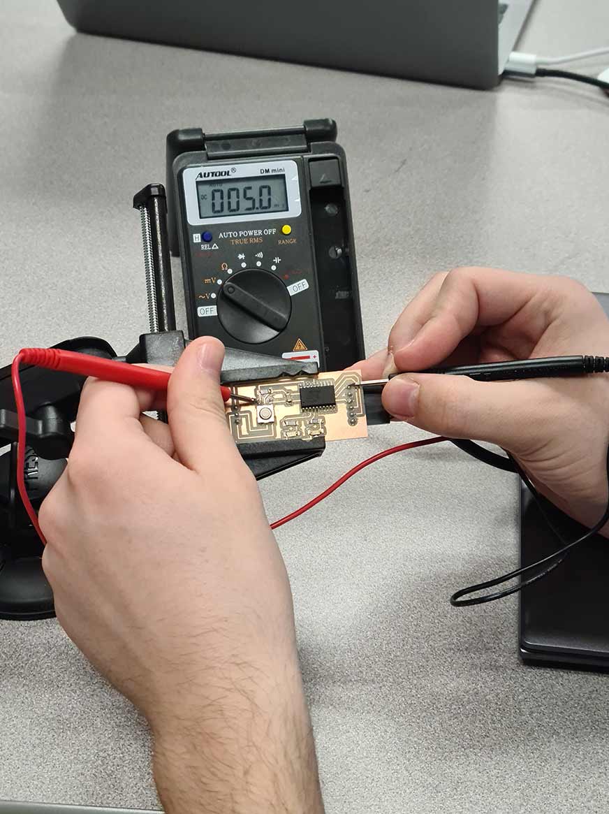
The group project this week was to use the testing equipment in our lab so that we could test our own boards. The equipment that we learned how to use was a multimeter and an oscilloscope. The image below is us reading the TXD pin of the attiny.
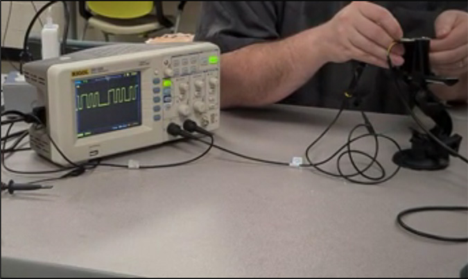
the image below is us reading the logic curcets of the attiny
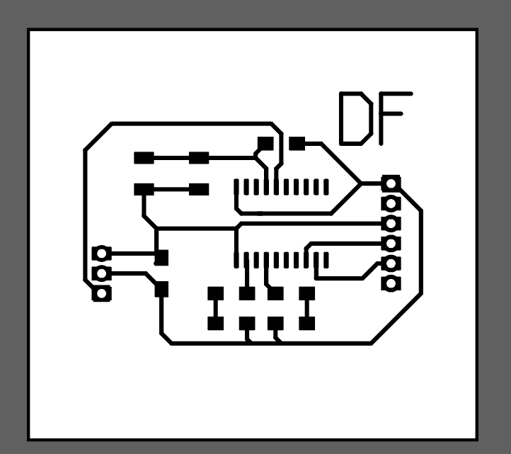
My Bord
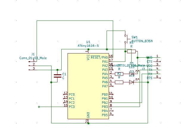
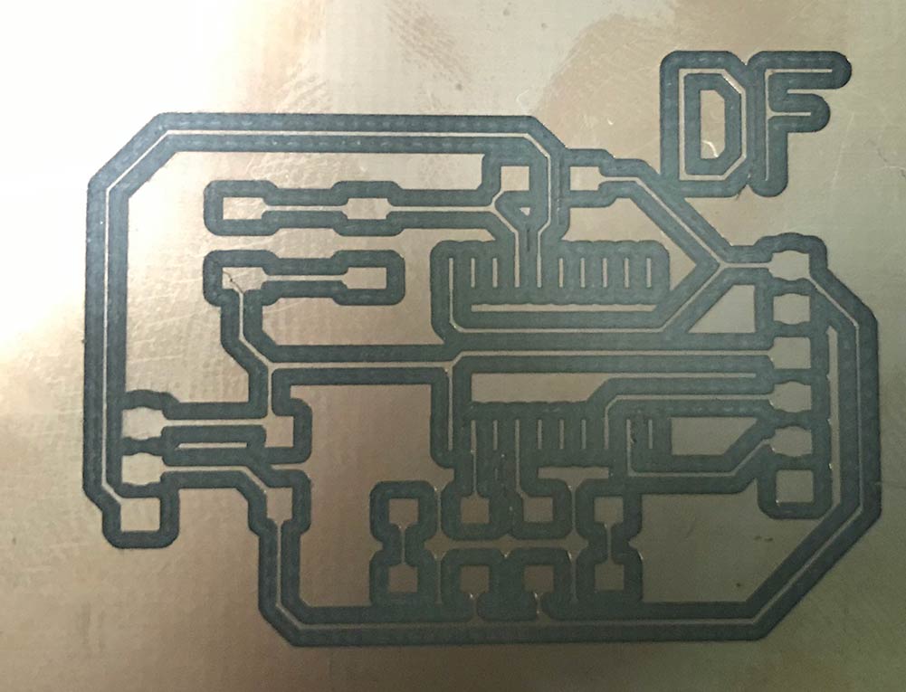
The individual assignment this week was to plan and make abourd from an image given. To make the plan for the board I used KiCad. The first step was to make the relationships for the parts that I wanted on my board. Here is an image of the relationships that I used for my board. I have two LED setups on ppin 2 and 4 with a buton with a pull down resitor onpin 17. It was rilly helpful to downloaded the fab acadimy part lidrary this is becuse of the amount of parts in KiCads defalt lidrarys.
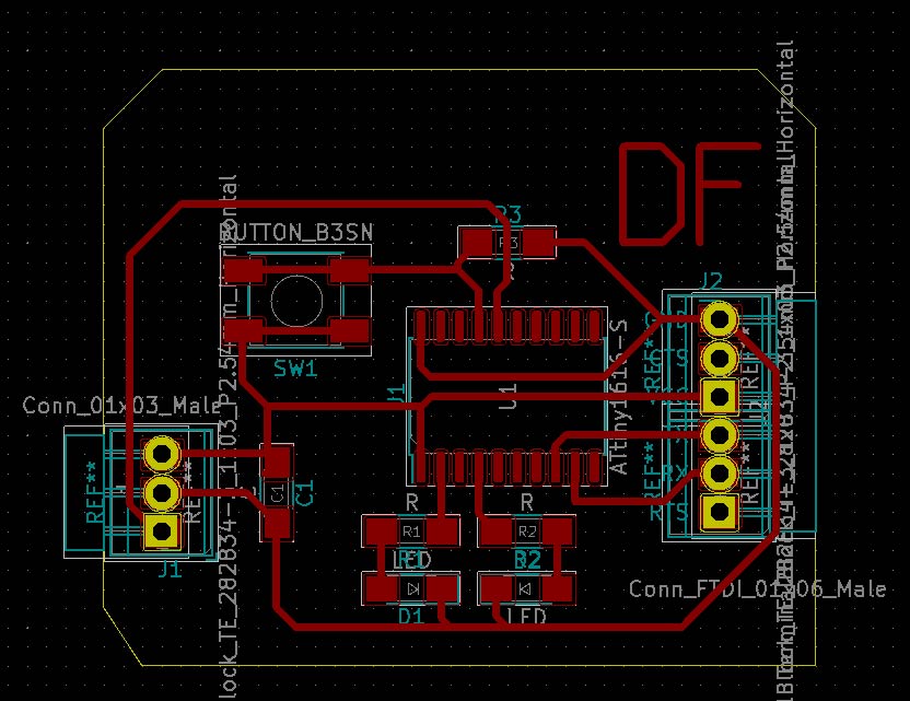
After that I used the tools in KiCad to make the board layout below I had a problem with the size of the 6 pin throw component so i used two 3 pin thru hole components instead. routing the traces on the bord is fun.
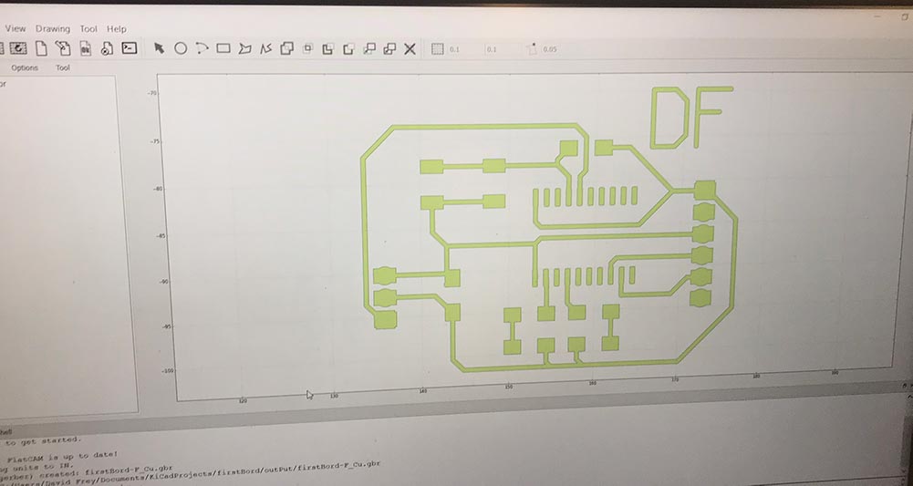
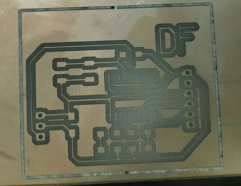
I struggled with milling my board. I tried mods and was not able to get it to accurately convert the traces around the attiny so I decided to use flatCAM. Here is an image of what I tried to put into mods and also my hole layout. the way that I generated the hole layer for mods waas I used the b.c tab becuse holes go throw the hole board.

this is an image of the start of flatcam after inputting all the files needed from KiCad. this is the traces generated from the gbr by KiCad.
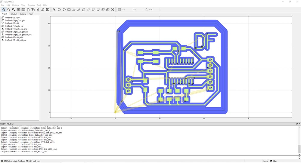
flatcam looked like this once i was processing the cut files for the traces, holes and outline.
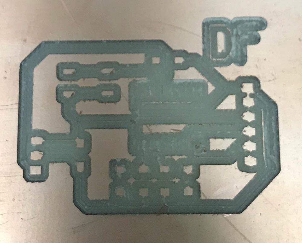
I made a mistake using flatCAM because I set the cut depth too deep into the board. but after fixing that I was able to mill a board. The image below is from the failed print attempt.
here is the board that I successfully cut out before I cut the board out and the holes into the board
here is the board before I removed it from the mill
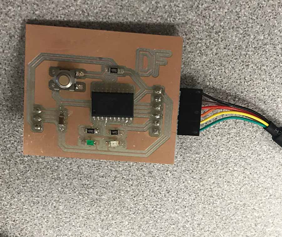
here is the board plugged into a computer with all the parts sotered on.
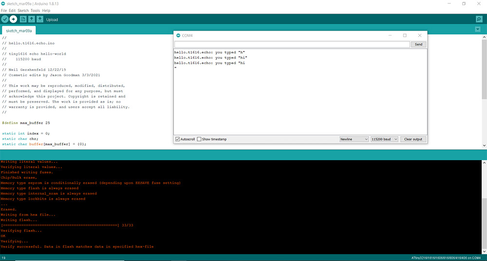
here is the screen of the successful upload message and the message that was returned from the board. the code that I downloaded was the ecco code provided by my instructers.
here is a link to my files look in week 6 folder for this week's files.
here is the link