Task to be Perform for this week
This week our task is to study Some desing rules for PCB(Printed Circuit Board ) and to Develope ,test the circuit programmer by milling and stuffing the PCB.
In this week we have to perform the Group as well as Individual Assignment
Group Assignment:-In group Assignment we have to characterize the design rule for PCB production in our Fablab-0. In which Check the various parameter of milling machine SRM-20 available in our lab.so we have to study the parameter like co-ordinate system, working area, offset, track limit for milling, the speed limit in our group assignment.
Individual Assignment: In case of individual assignment I have to make an -in-circuit programmer using SRM-20 milling machine, also I need to practice on how to mount different component on PCB and to learn the techniques of soldering and disordering
I really enjoyed the assignments and soldering, and there were big challenges during the week. However, I need to practice soldering to make my joints beautiful.
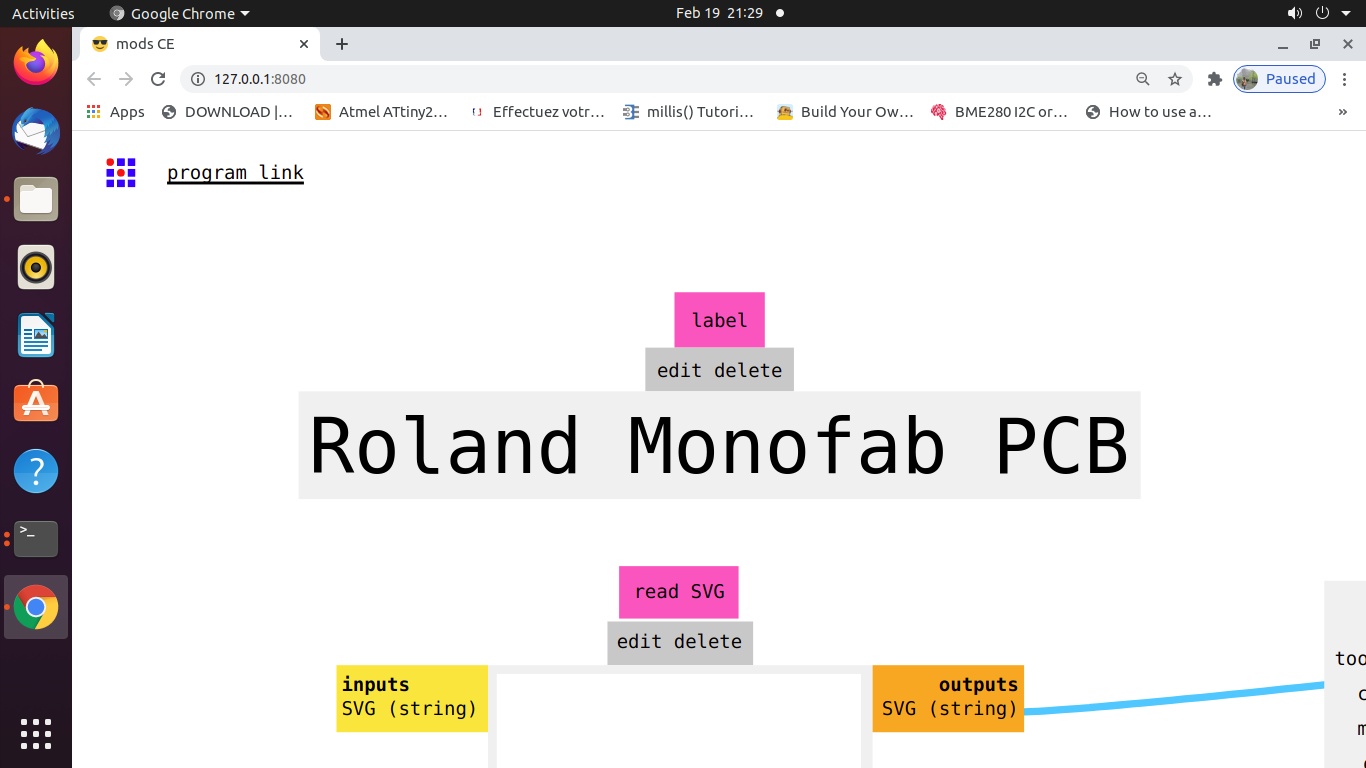
Learning outcomes
1) Described the process of milling, stuffing, de-bugging and programming
2)Demonstrate correct workflows and identify areas for improvement if required
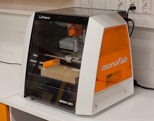
ABOUT SRM-20
As we know the PCB manifacturing process is very importent for electronics industries. PCB's are generally use to built the basic electronics circuits
The PCB milling machine available with has specification below:-
Manufacturer: Roland
Model: SRM-20
Specifications: 203x152x60 mm, 1800 mm/min, 0.001 mm/step, 7,000 RPM
Applications: Precision three-axis machining, including PCBs down to 0.25 mm feature size, and machineable wax to make tooling for molding and casting
Group Assignment :-
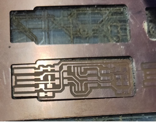
In group assignment, We have to study about characterize the design rules for PCB production process.So in group we have tried to machining of PCB using milling machine SRM-20

We find the width of traces that can be mill on srm20 milling machine.
The details about Group Assignment
Click here to detail about Group Assignment
Summary: In group assignment we can conclude that if the distance between the traces is less than 0.0156mm (i.e.diameter of milling bit "1/64") the machine will not milled it.
Individual Assignment:-
In case of individual Assignment we have to make an in-circuit programmer by milling and stuffing the PCB, test it, then optionally try other PCB processes.so first i have tried to use FAB ISP for the process.
FabISP:- The FabISP is an in-system programmer for AVR microcontrollers, designed for production within a FabLab. It allows you to program the microcontrollers on other boards you make.
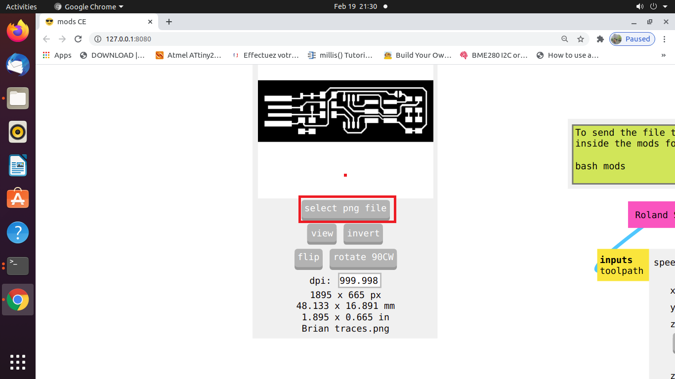
At initial stage I need to download the file Available in png. format from Fabacademy websites
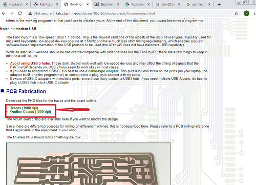

PCB Fabrication: Making an in-circuit programmer "FabISP"
Basically the PCB is nothing but the printed circuit board which is machanically support and electrically connected electronics component to form a electrical circuit.
The FabISP is Brian's version of an AVR ISP programmer/board which one I chose in order to produce a milled PCB with some basic components.
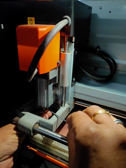
Preparing for milling machine Ronald SRM 20
After the global review we were introduce the milling machine by our instructor available at our fablab
Step to configure the SRM-20 with Ubuntu.
1) Boot the Desktop terminal using Ubuntu OS.
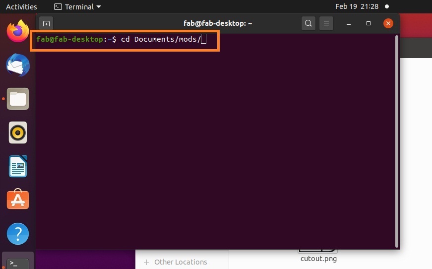
2)Open Terminal and use commands
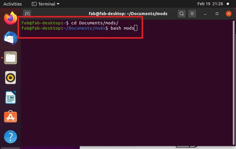
cd Documents to change directory.->mods->>bash mods
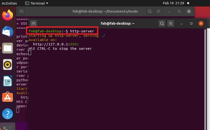
Again Open New Terminal and use commands
Cd Documents -->http – server
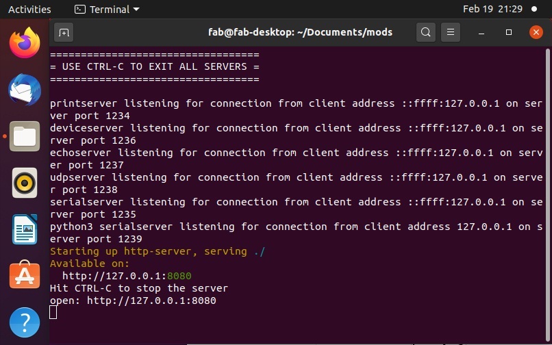
3) This will open a Window in Google Browser.
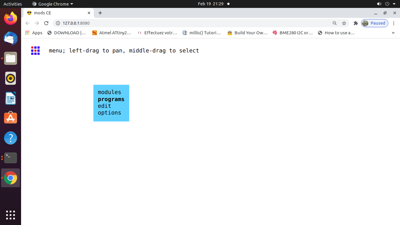
4) Right Click in the Window
Four options will be displayed like Modules, Programs, Edit, Options etc.
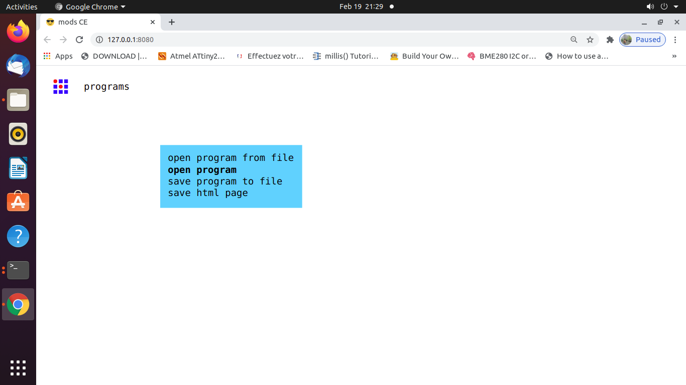
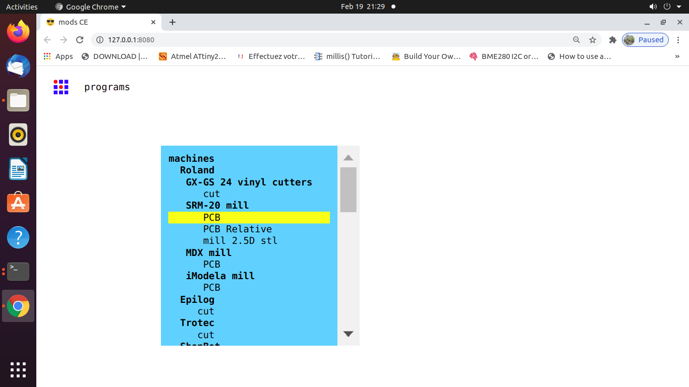
Select Program-->Select SRM2
5) Select the Image
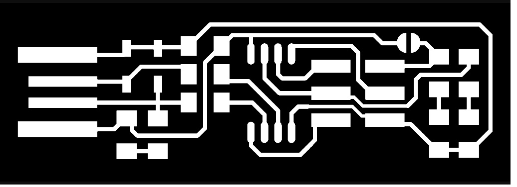
Check the format of the image (.png)
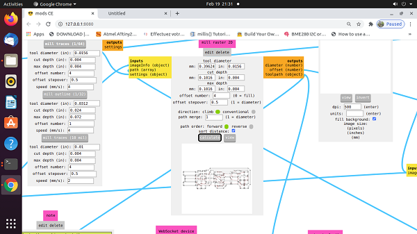
6) Select the mill trace 1/64” for PCB traces
7) Select the mill outline 1/32” for PCB outline.
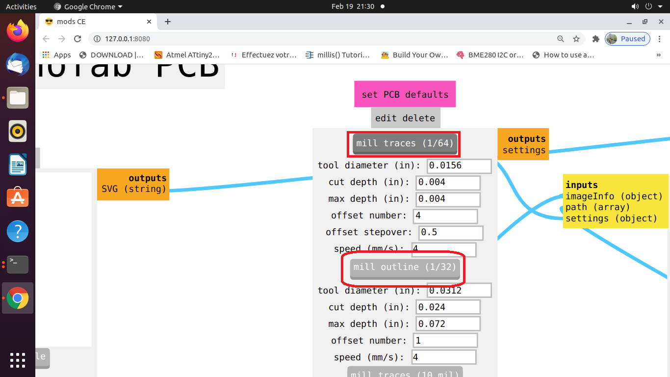
8) Once we select the drilling bit all the parameters get set with its standard value.if any one want to repassed then you can changed the parameters.
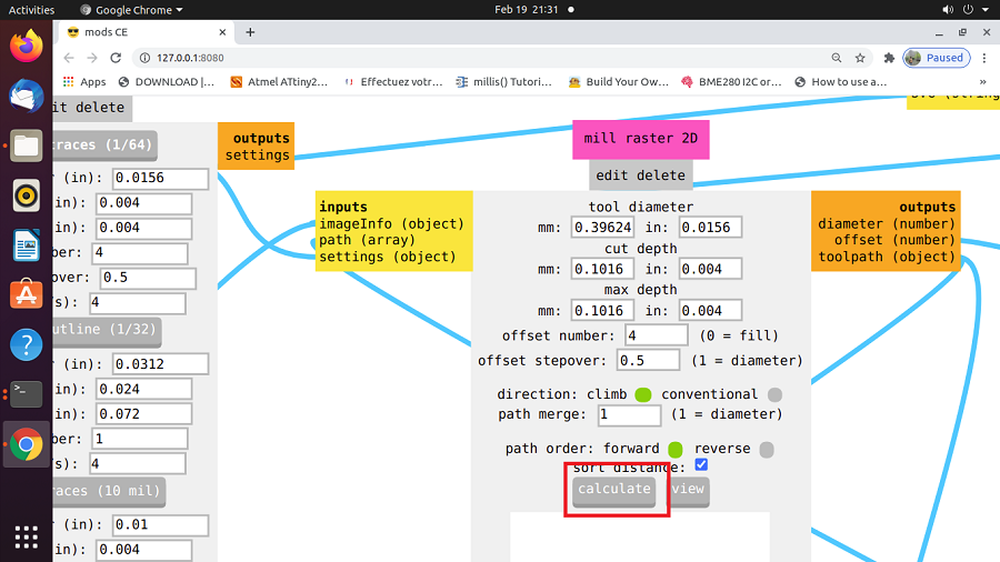
Select the calculating option.we can see the path of our module program the way through png image converted into rml the language under stood by SRM 20 machine.
9) Click on the open socket.
10) Set the origin at home position, then set according to X, Y, Z axis position.
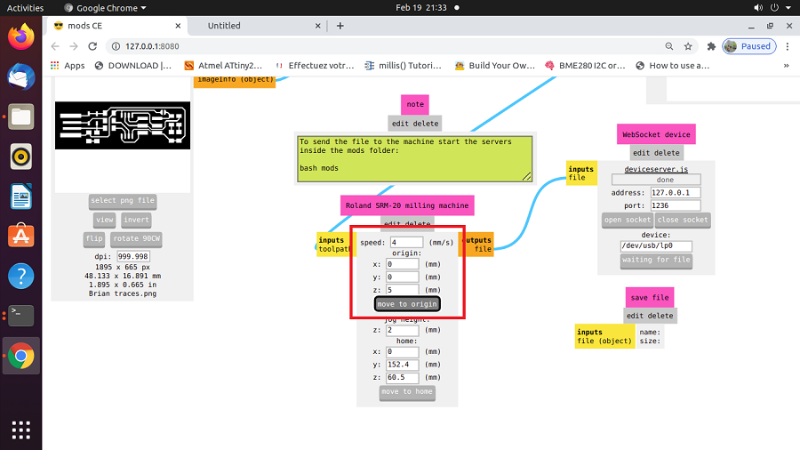
11) Note that drilling head moving along X axis, Bed moving along Y axis and Drilling bit along z axis.
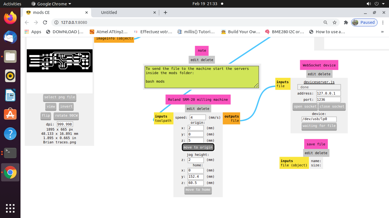
12) Again click on calculate , it will trace again. Click on open socket and finally click on send file to device.
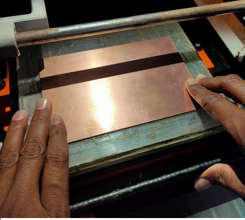
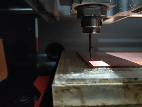
Place PCB Sheet
Initially i have to place the PCB to prepare the machine for milling
1) First we need to open the door of machine set the proper beding.
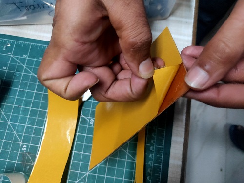
2) we have used Sacrificial Layers of acryilic material for proper beding.
3) Then take the PCB - in our fablab have FR-1.
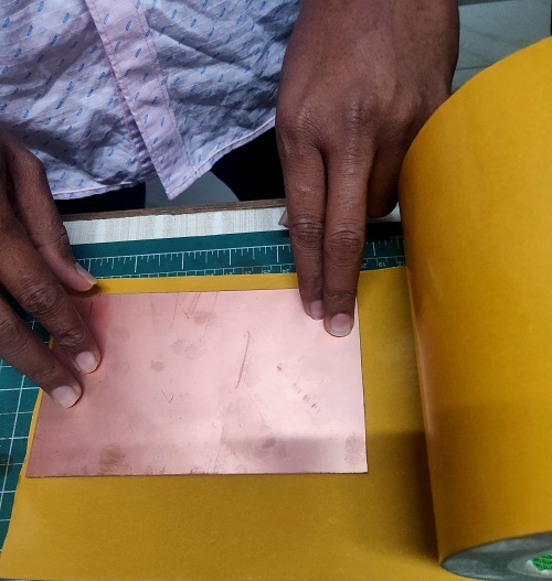
4) Then turn the board upside-down to see the background and put double-sided tape stripes carefully above it. This is a crucial part and they cannot overlap at all since otherwise the board will be bended. Cut the extra tape off from the sides and clean the board properly.
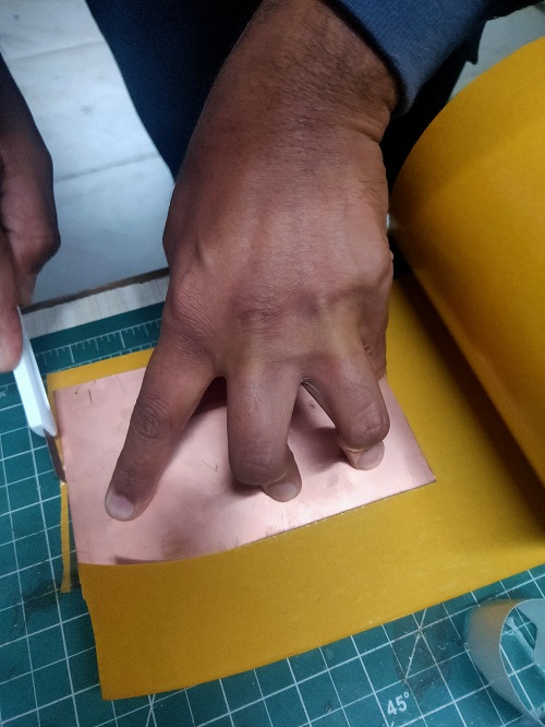
5) After that carefully Check the surface of the plate, which has to be absolutely straight and level.
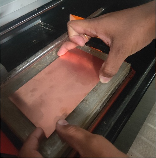
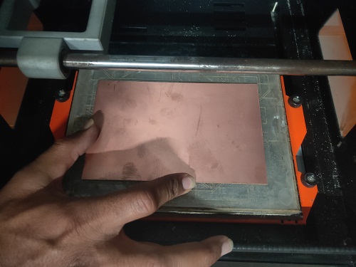
6) Finally do the proper beding of PCB board into the machine
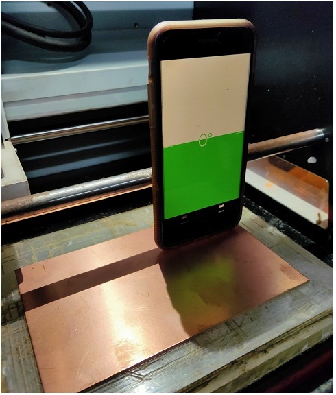
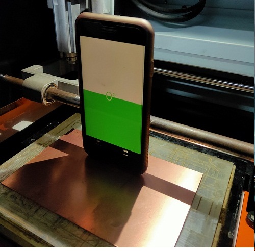
This is I have checked the leveling of bed
Inserting a Milling bit
1) First off all the two types of milling bit we need to use for the process.
2) 1/64” bit for traces carving, and 1/32” bit for outline cutting.
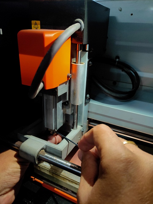
3) The bits is very brittle (especially the 1/64”) So while inserting the bit, remember to holding the bit while Loosen the small screw in the shank by allen key. This is to avoid the bits from falling and break itself.
4) Then need to Change the Z axis from properly to make sure the bit is touching the board.
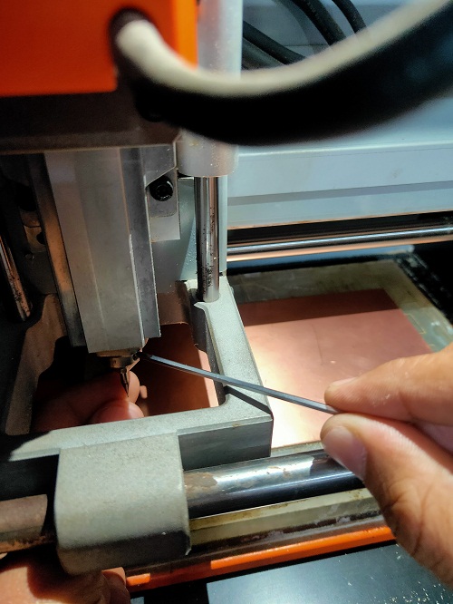
5) When carving the traces, use a plier to push down the bit to make sure the depth is approriate. Otherwise there will remain some shiny parts.
6) If the motor doesn’t response, restart the machine
SODLDERING PROCEDURE
Before this task I have known some what about the soldering for Zero PCB's
So it was quite difficult to me becuase here i need to use SMD component.
Used some basic SMD electronics component and tools for soldering.
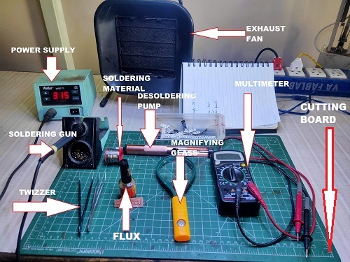
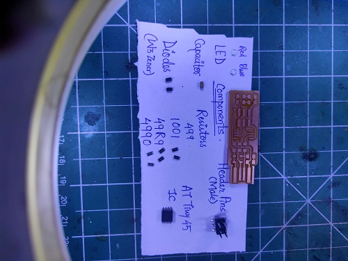
Electronics Component to be used for ISP (In circuit Programmer)
1) Twizzer : -When sodering the any SMD components on PCB it is diificult to pick or hold the component and to soder in it correct possition for this case we need twizzer for pick the component easily.
2) I have also used flux on the PCB it is useful to made a strong bonding of electronics component on the copper. I have used tin lead material for sodering
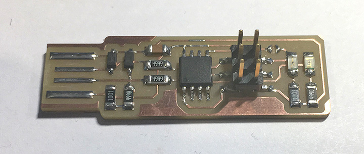
3) For soldering i have to stuff all the component on PCB board.
4) Then I have to checked the polarities of component like diode, LED's and the pin diagram of IC i.e. Attiny45
After that started the soldering by connecting one by one component on PCB
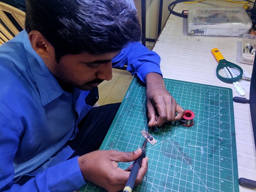
4) finally connect all the component presizely make sure that there is no any shortcircuit
After soldering my PCB looks like
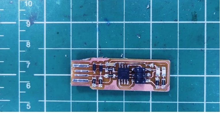
Here, When i completed the soldering and connect FABISP to my Laptop the LED was not Blinking because Diode connected in opposite polarities so i need to desolder and solder it again.
Again the soldering was not proper because i was doing the first time so i need to do more practice on it
Programming Through Software
After successfully completing the soldering process we have to program our PCB board through Linux or Windows operating system.
Fab Academy provides an instruction for software installation for PCB. All the instructions is vary as per operating system.
In our FABLAB Linux operating system has already installed on computer as we have already done the group Assignment on this PC, I have Programmed the PCB on my own laptop Using the GNU AVR toolchain on Windows 10
Go to fab academy website, in 2021 assignment menu click on schedule. In schedule click on week 4 electronics Production assignment--> In individual assignment --> click on In-circuit Programmer-->In system development click on Brian--> In software Installation click on installing the tool chain on Windows is slightly more complicated.
Then click on here
Steps to follow The Git Bash through Windows Opertaing System
In my own laptop as I mentioned my windows operating system is windows 7 /32 bit so i have tried the below steps for installation.
1) Firstly we need to instlled the GIT Bash , As we have already Git bash so click on start type git bash and open it
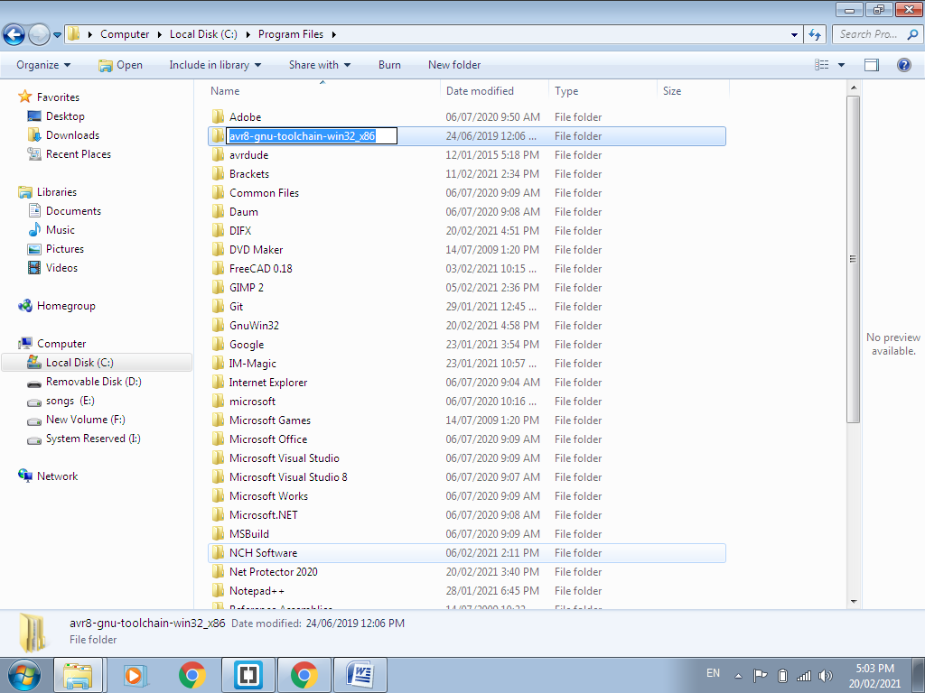
2) Then I have Download the Atmel GNU Toolchain Windows from Atmel's site and run the installer.
When asked where to extract the files, click the "..." button and navigate to C:\Program Files, then click Extract.
3) Download avrdude.Unzip the archive, and copy the archive inside to C:\ProgramFiles.
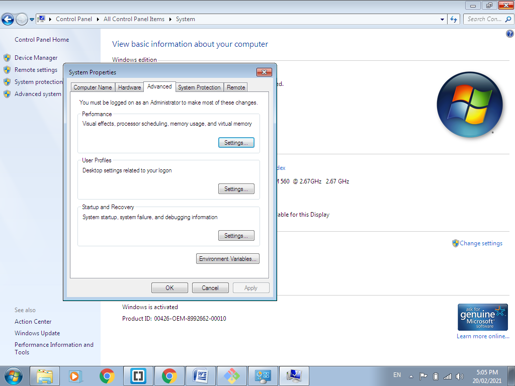
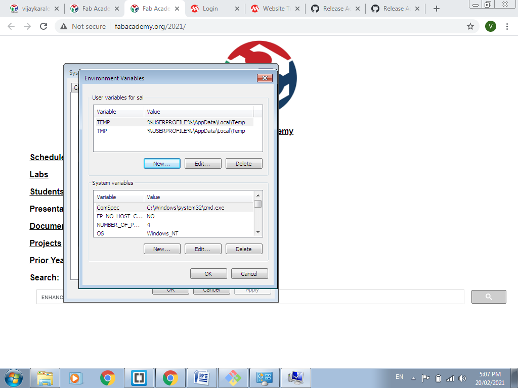
4) Then go to the Start menu and search "Advanced System Settings". Under the Advanced tab, click the "Environment Variables" button
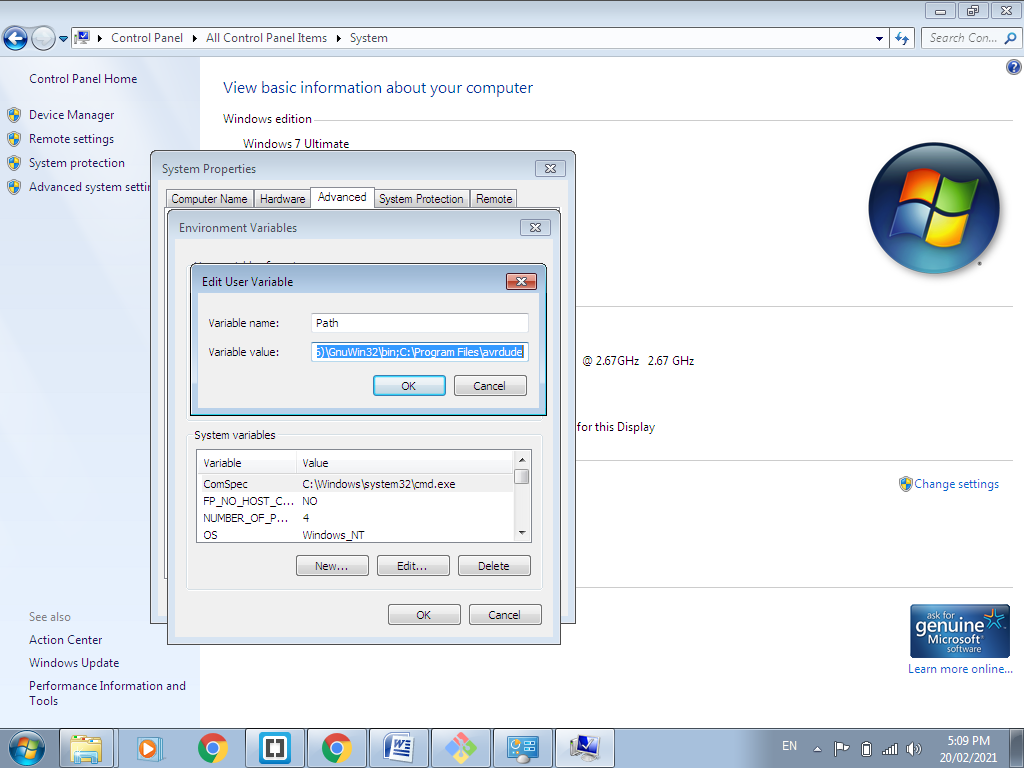
5)Under User variables, select "Path" and click the Edit button.
Here i have faced the problem in my laptop there was no such variable "Path" so i had to create the path veriable first
Note:If you don't already have a variable called "Path", click the New button to create it, enter "Path" without the name, and fill out the value as described below.
The three values to add are:
C:\Program Files\avr8-gnu-toolchain
C:\Program Files (x86)\GnuWin32
C:\Program Files\avrdude
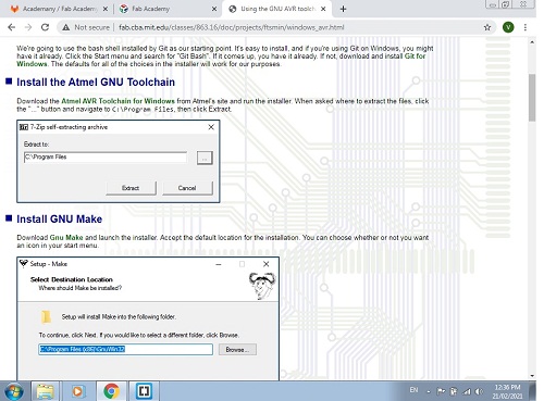
This is for GNU make SETUP
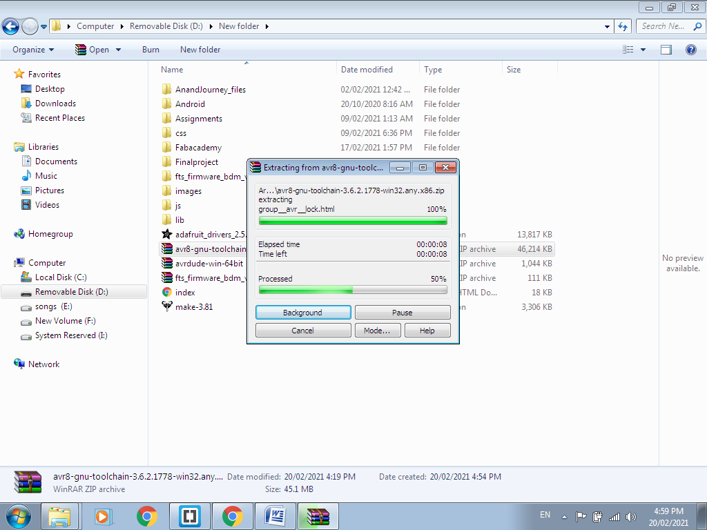
This is for extracting the files in C Drive
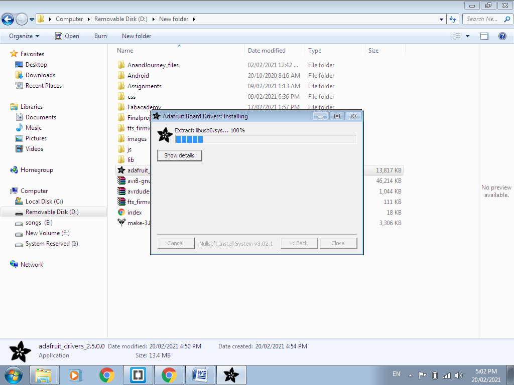
I have installed required USB Drivers also as it was showing need to installed the drivers form Adafruit
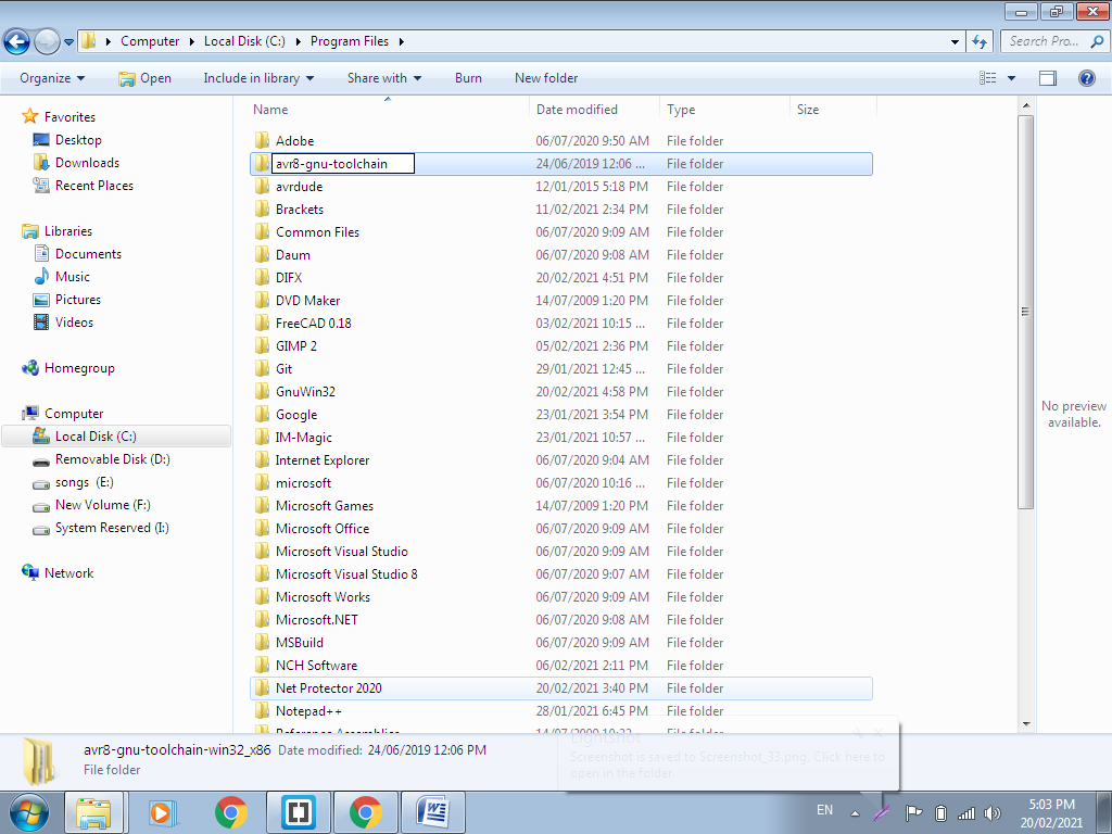
Then need to rename the file with avr8-gnu-toolchain
This is for giving the path
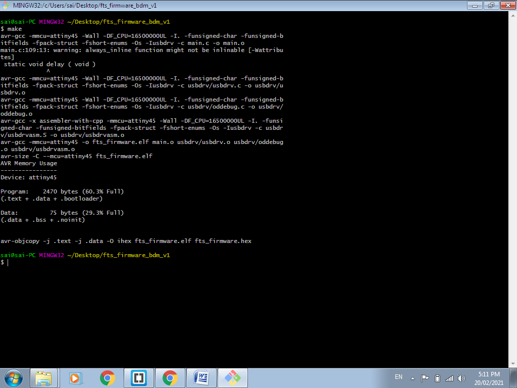
After compliting the installations of above files go to Get and Build the Firmwire: So i have Downloaded the firmware source code and extract the zip file on my desktop
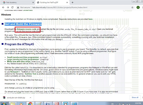
Then open the git bash from start menu apply The command Desktop/fts_firmware_bdm_v1" and then press enter
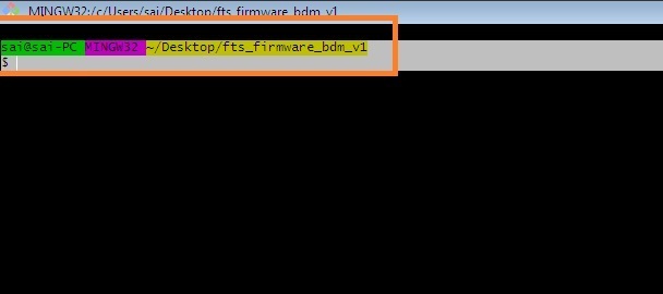
Then type "make" in the command windows and press enter:This will build the hex file that will get programmed onto the ATtiny45
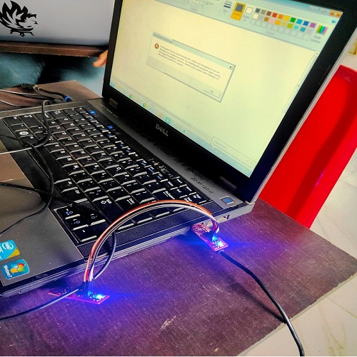
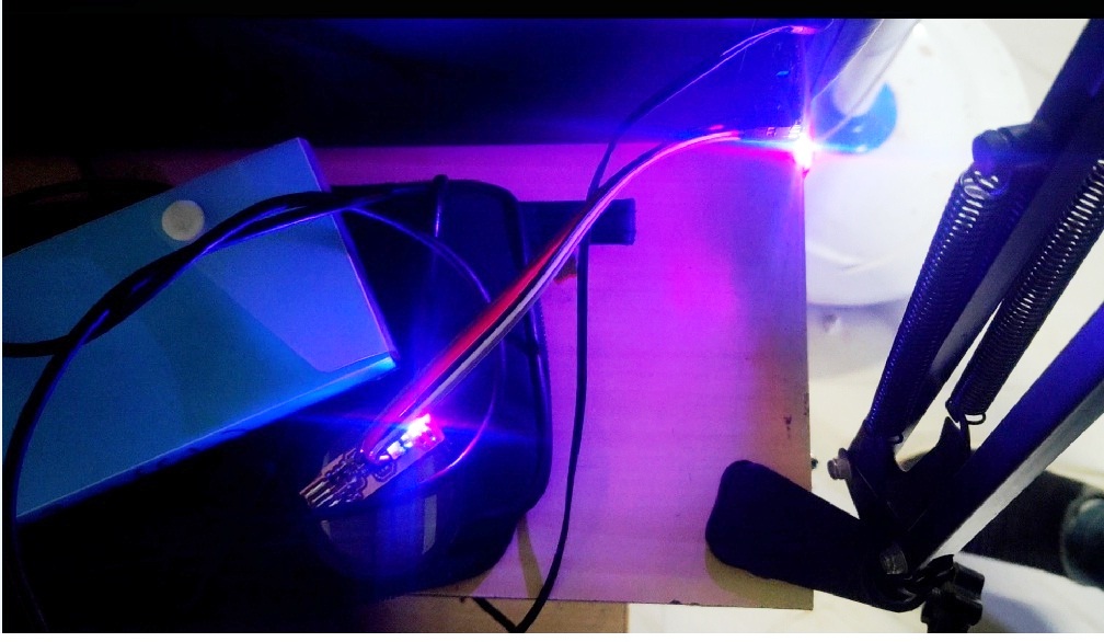
Now, I had to interface my FabISP to laptop with anather programmer through connectors.
The LED will glow in both the PCB's means connections are correct.
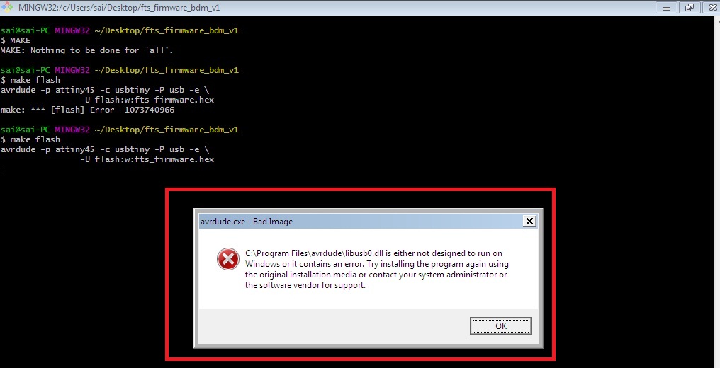
Then Run make Flash command:( As my windows 7- 32 bit operating system it gives the error in my laptop it was not supported to my system
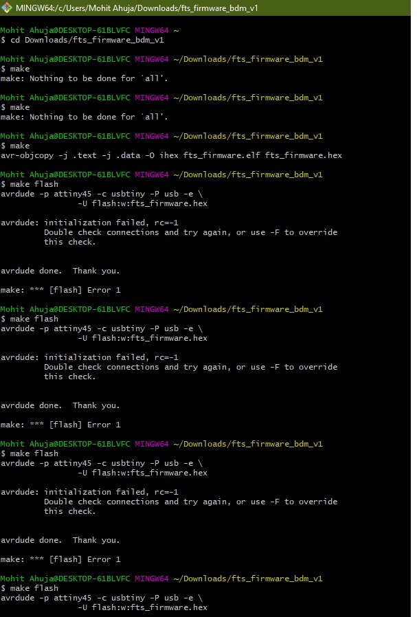
Then I have tried to program the PCB on my one of my friend Mr. Mohit Ahuja's computer system as he had winodws 10 ooperating system
I have follow the same steps on his system
This is to run the make flash Command: Initially it was showing avrdude sucessfully connected but giving some error initilization failed "Double check the conection"(For this case i need check the connection
So, I have checked all the connection and be sure that all component connected properly on PCB:
Run the make flash command again:(This will erase the target chip, and program its flash memory with the contents of the .hex file you built before. You should see several progress bars while avrdude erases, programs, and verifies the chip)
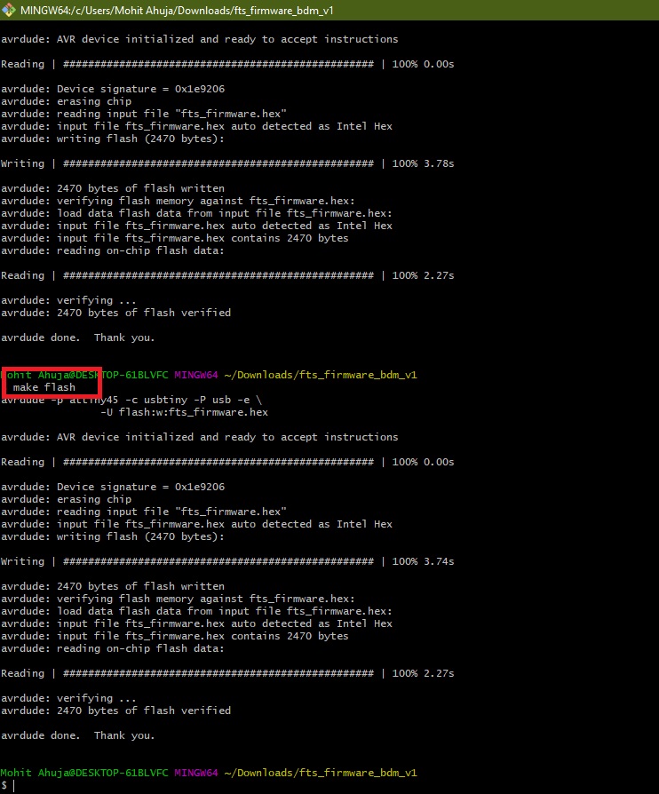
Yes its done,succesfully programmed the flash memory
Now its times to configure the fuses
This will allow us to check that the board works as a USB device, but it won't yet be able to program other boards.
So i have run the make fuse command in command lines
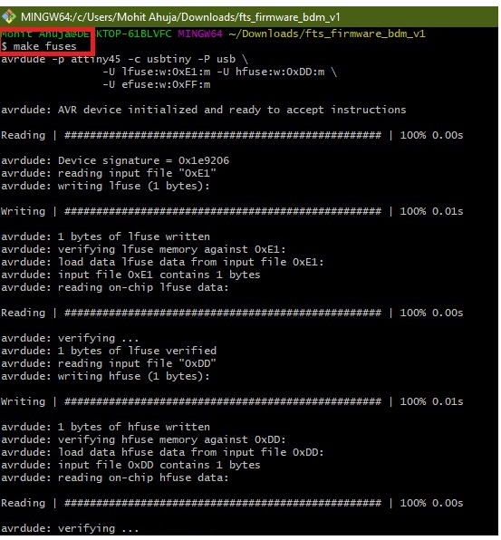
This will set up all of the fuses except the one that disables the reset pin.
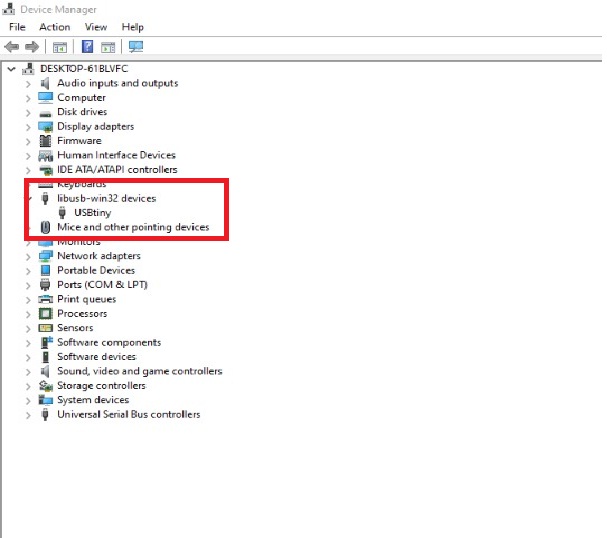
Now, i had to Check the Functionality of USB,
for this Unplug your board from the USB port and disconnect the programmer, then plug it back in to the USB.
Now go to device manager from Control panel (Start → Control Panel → System → Device Manager)
Lets check program is sucessfully or not by directly conecting the ISP to laptop then the laptop shows the USB device is connected
In that it was showing USBtiny
Now its almost to a working programmer. The ATtiny45 on the board has the code loaded onto it and is working correctly.
There are two final steps left to turn your board into a programmer that can program other boards SO I have tried first step only.
I need to change the bit that will turn the ATtiny45's reset pin into a GPIO pin.
This will disable our ability to reprogram this ATtiny45 in the future
This case i had to connect my ISP programmer to your board one more time, and run make rstdisble.
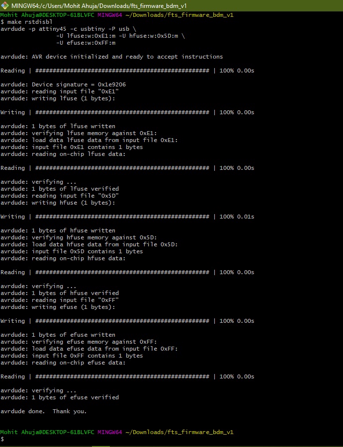
Now ,avrdude will never be able to talk to this chip again through the ISP header.
What i have learned ?
In this Week Assignment I have Studied
1.How to Charaterize the design rule for PCB production process by using SRM-20 milling machine.
2.How to use Mod's for conversion of png file to rml file.
3. Studied about Machining of PCB on SRM-20 milling machine.
4. Hands on pratice on PCB soldering, component anode and cathod point indetification, conductivity testing etc.
5. FabISP programming using Windows10 operating System system.
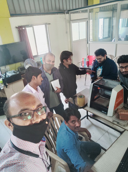
In this week I was reviewed by Professor Neil, link of my globle review Here
Downloads
Download my original file here