Sixth Week:
Electronic Design

To this assignment we had to design our board and included a button and a led at least. I used this escential tutorial from Fab Academy that I personally recommend to learn about the electronic devices and assest I used in this page.
Practicing... "The more you practice, the better you get"
Due to pandemic situation was not possible for me to go to laboratory so I was practicing at home in a helpful software, part of Autodesk, Eagle which you can get free with Fusion 360 1-Year-License of Fab program.
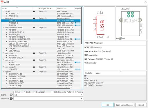
Now it's time to fill its default repository with device you will use so we have to choose which ISP we will build, at my case I selected David's ISP. I couldn't get, at the time I was doing this assignment, the total of available pieces and device I would use for pandemic restrictions. Beside of that, I tried to use same or similar pieces which David had used in his ISP but I didn't know where and how to find those files, hence I went to a FAQ where I could find some information as you can see in th next picture.
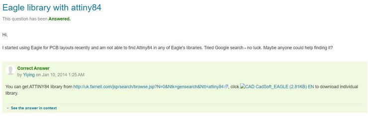
Following some instruction I could find my files here Farnell, which is a emarket where you can find the files you would need or similar as my case and then integrate at your Eagle. Letme show you how.
1st. You have to search the componenet you will need.
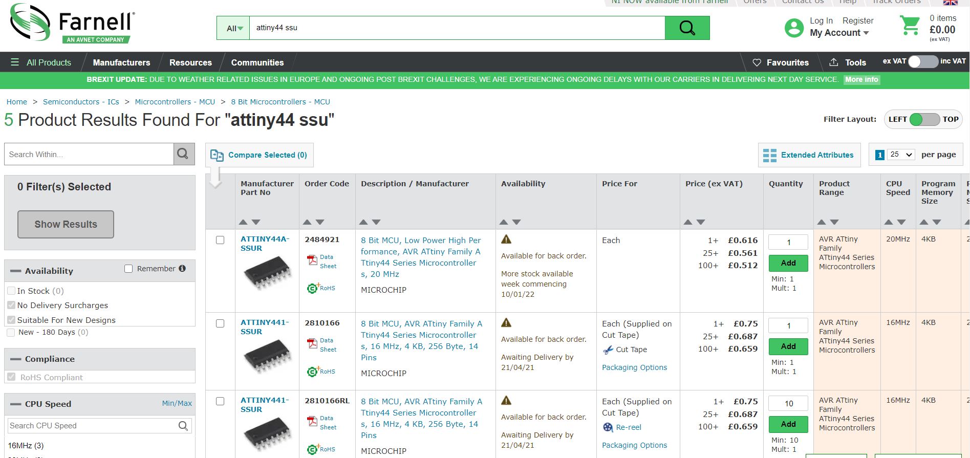
2nd. You have to select the exact or similar component, I chose an "AtTiny44A-SSU" which was a similar one but not the specific.
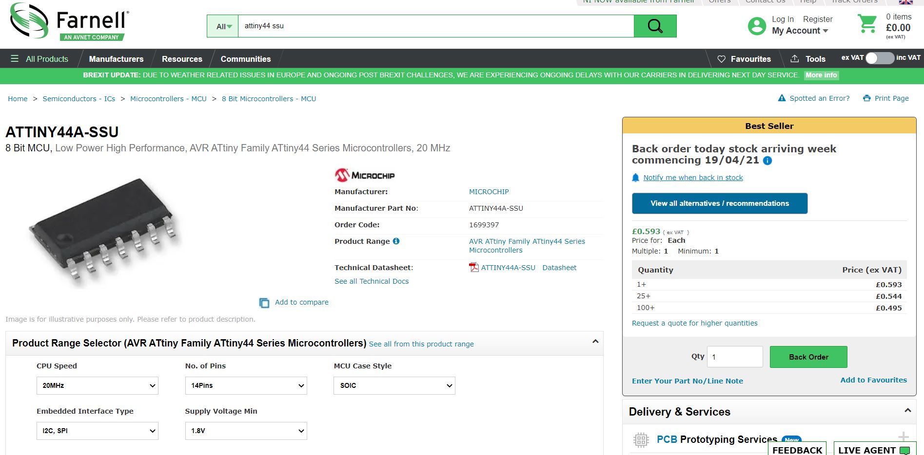
3rd. You have to go to the bottom and select the file called "CAD CadSoft_EAGLE" or similar, this file and format is the required.
4th. You will have to decompress. As a result of that process you will have a folder with these files.
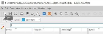
5th. We have to go to Eagle interface and on left-above we will choose File and "New library".
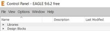
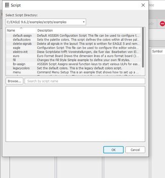
6th. At this part we have to select the blue icon with "SCR" layer, this open "scripts" files which are assets to Eagle.
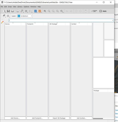
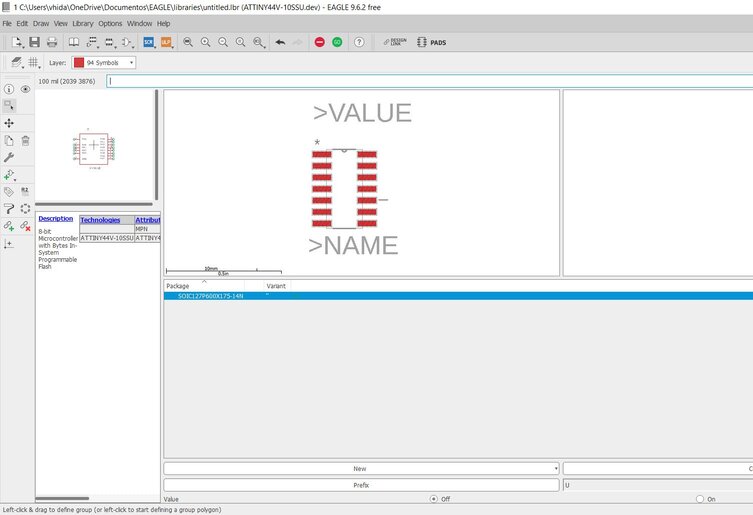
7th. We have a box where we will go to "Browse" and then we will import our files, I imported my "AtTiny44A-SSU"
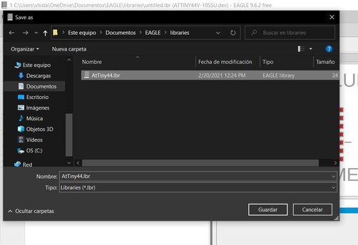
8th. Finally we have to save as a library, we have group lots of assets to create our own library.
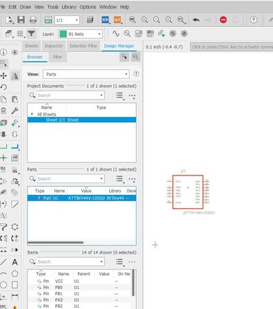
So, it's time to start the designing process. For this part we have got "Files / New / Schematic" on Eagle's interface. Then, at this new window we have to import the assets and devices required for our project following these instructions.
1st.- We have to click on this icon at left side of "Schematic" window.

2nd.- We have to select which piece or asset we will use, just one piece each time you cannot choose a group.
3rd.- We will finally have to paste it on the board and start the designing.
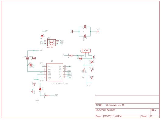
After all the designing process we will have something like this.
Note: I highly recommend to watch some tutorial at YouTube or research and read information or tutorial at some Eagle's Forums.
Now comes the board designing part. So, we have to convert our schematic into a board select an icon on "Schematic Eagle" window.
In this part I had some problem when I tried to move assets to repositioning as you can see and it was later when one member of my lab told me what I was doing wrong.
Recommendation for this designing part is to practice, this interface will be guiding you where to put the "connection"/"wires"/"awires" and you can use helpful, to practice, tools as do some holes and make those electrical connection. In my case, at that time and that "unknown" problem, I decided to make a 2-faces board as you can see now.
Note: You can select the face at this part of the interface.
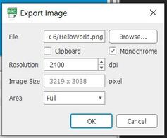
Then, we have to export the file as a ".png" format. We will do this at right side of "Board" window clicking on "Manufacturing" slide, this button is rotated. There we can change some color as parameter which will help some program to recognize and design a "G-Code" format.
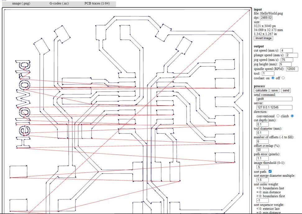
At this point we have a beautiful image of our board but we have to convert this ".png" format to one which our machine will be able to process. In my case in change the format in Fab Modules and did these next steps.
1st. We have to choose our input format importing our file as I did.
![]()
2nd. Now we need to select the output format, I chose G-Code ".cn" format.
![]()
3rd. It's time to select the process, I select "PCB Trace (1/64)" which is defined for the process and the machine. Next to, we have to fill some values and parameters that are part your specific lab machine.
![]()
4th. Click on "Calculate" to start the convertion process as you can see at next picture.
![]()
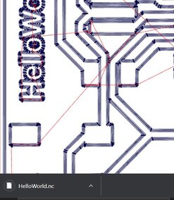
5th. Finally we will have some like this which is the final product format ".cn" so we have to download clicking at "Save" button.
![]()
![]()
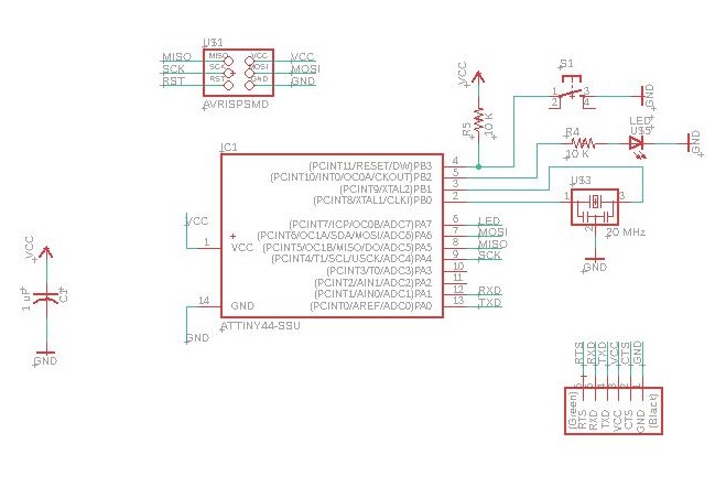
Designing the board
To this part I used Eagle from my Week 4 assignment. I based this design in my friend's board design just to understand.
First, I selected which parts/devices I will use. Then I connected them using some parameters, which were recommended.
Aditionally, I defined the name of the routes to make easier the building part at Board section.
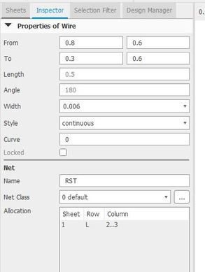
Second, I asked for support beacause I was looking for a way to use the button as a Reset Button. The person who was supporting me recommended me to use a Pull Out format.
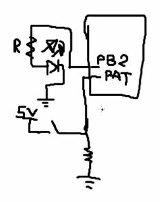
Note: This was an example to undestand the pull down system.
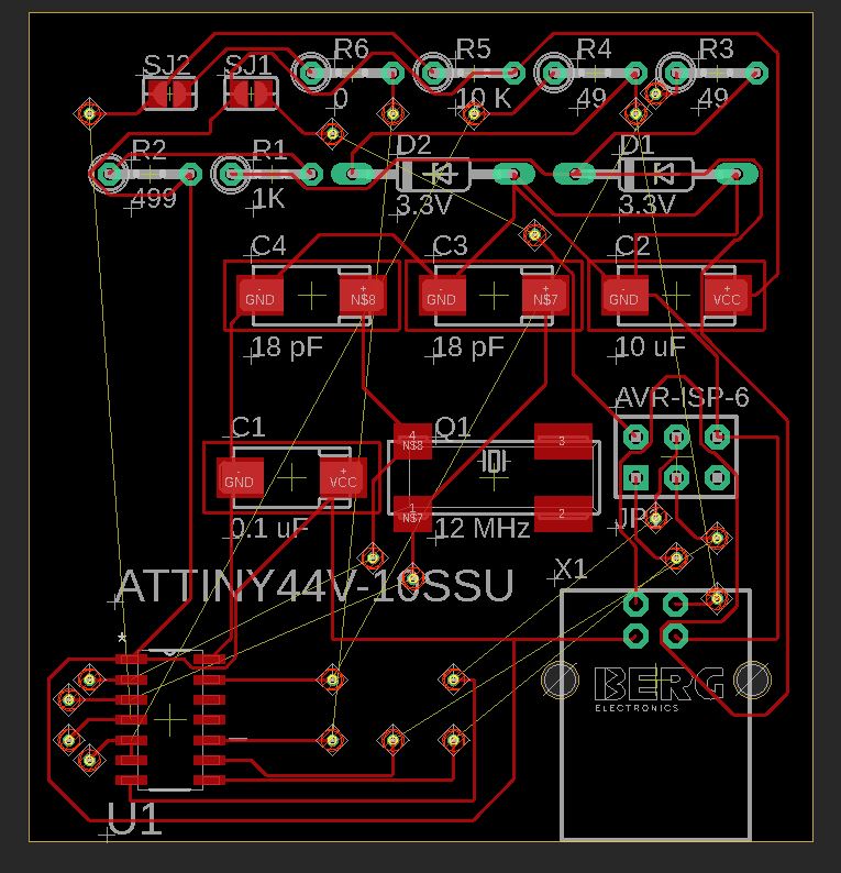
Having this understood I finally designed my pcb schematic ready to connect components at Board section.
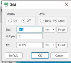
Now, I started with the board designing. To this part I used 2 parameters for the designing: the Grid's Size and the Widht, 0.1 mm and 0.4 mm respectively.
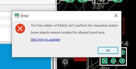
To this part I spent a whole weekend to find a way to conect all the parts. It was hard because there was always a device which could not be able to connect to the other. Finally, I found a way and could finish the design.
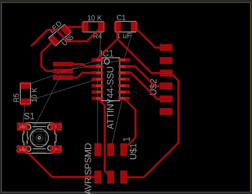
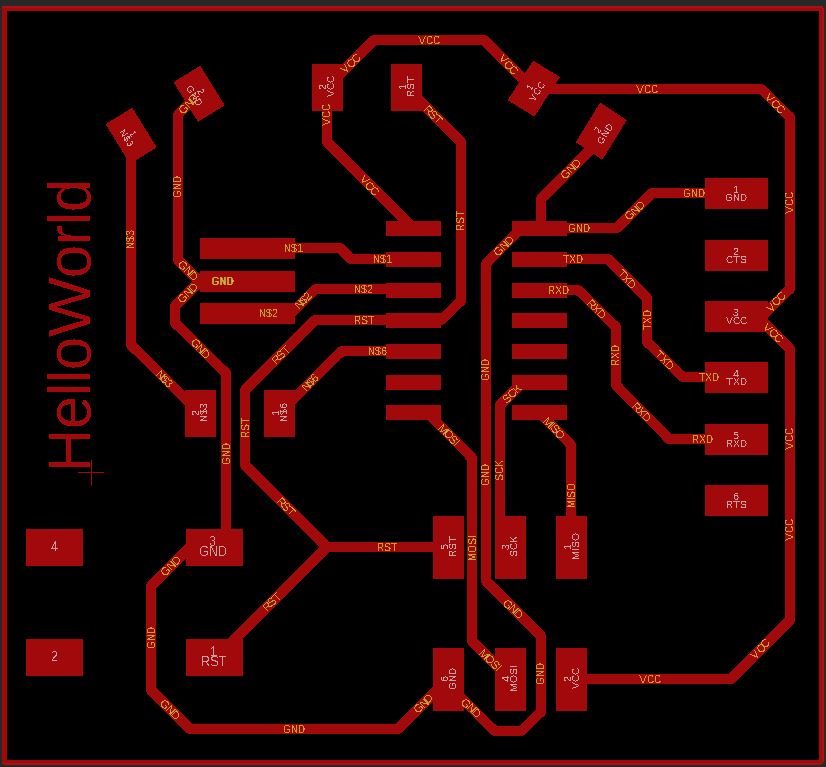
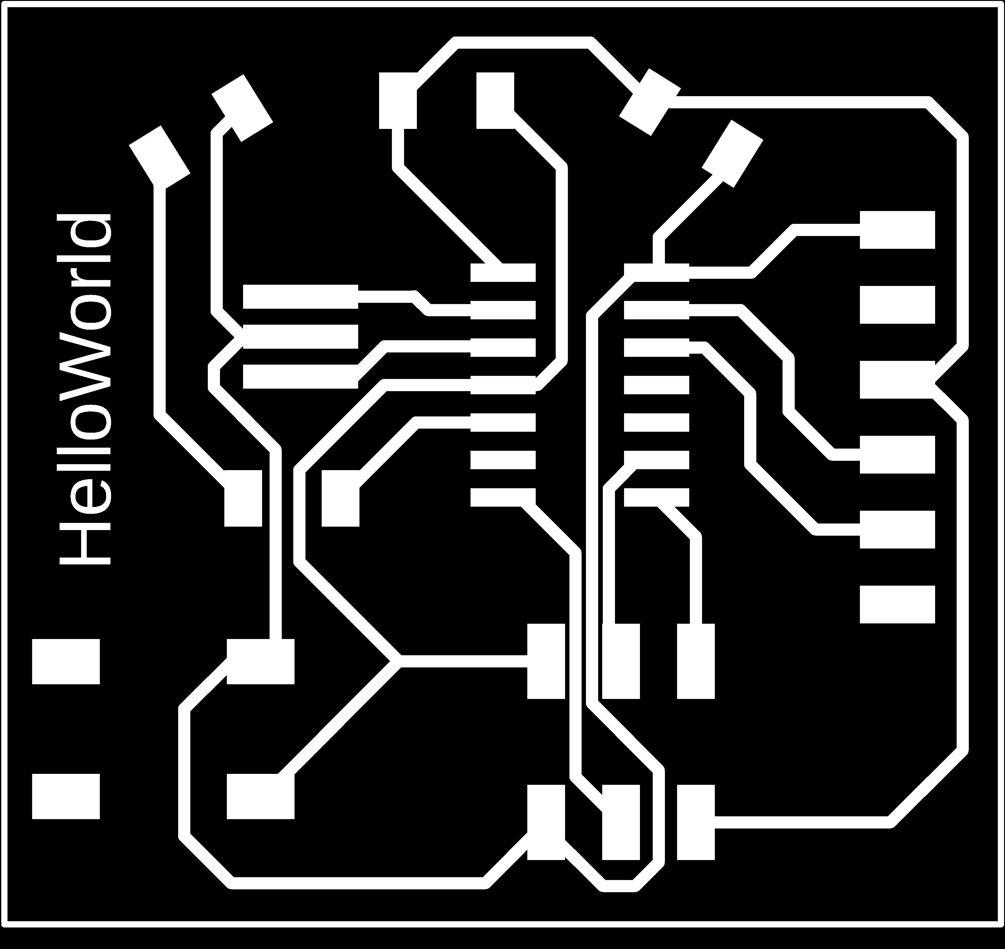
And I obtained this.
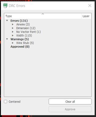
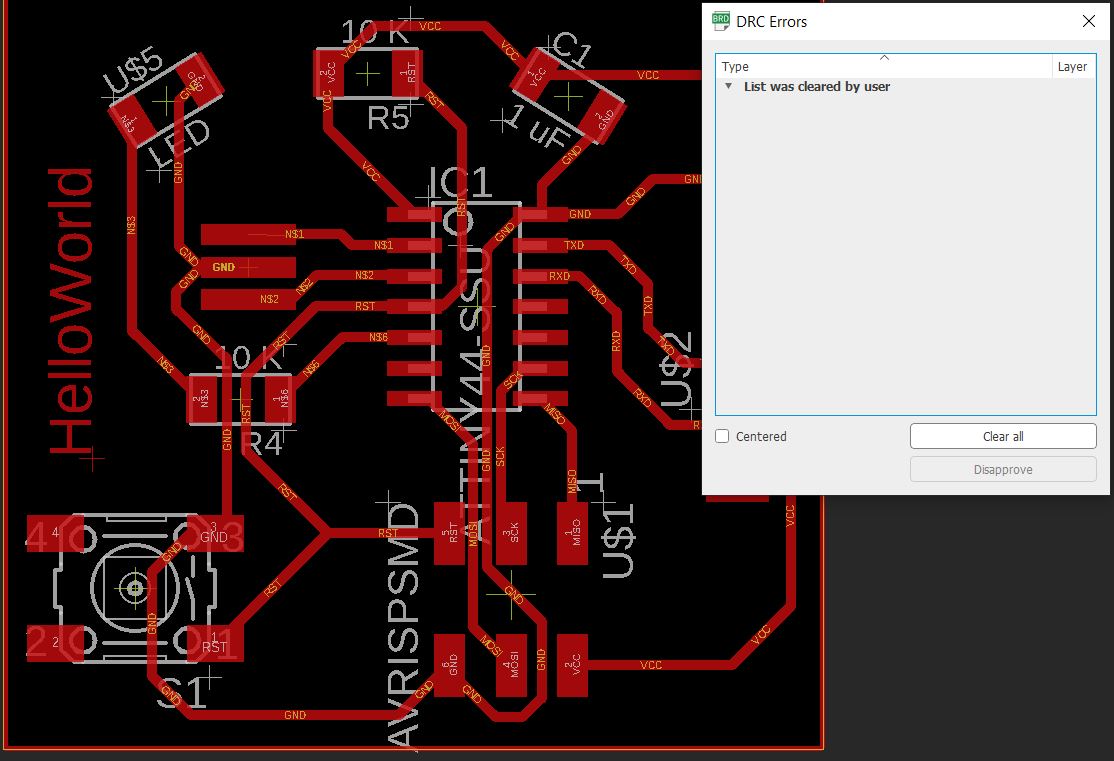
To check and correct some errors which can make problems I used DCR tools at Toolo section on the top part of the software.
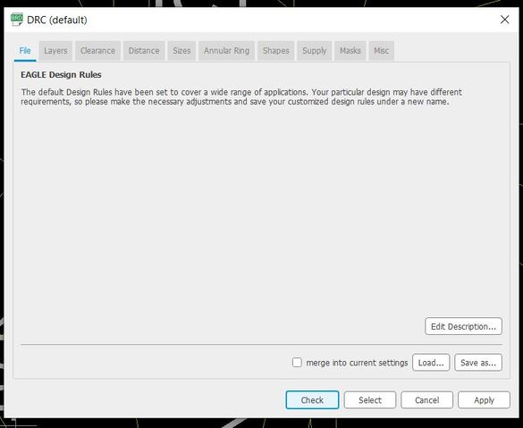
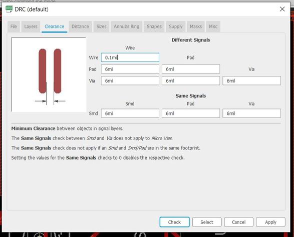
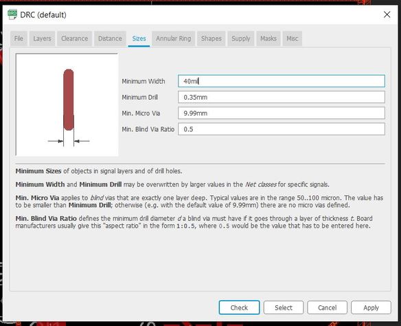
This window will apear where there will be the errors and problems the software found and a option to solve them.
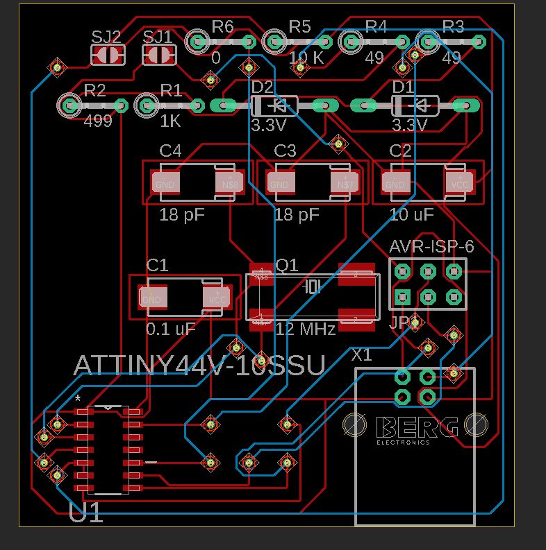
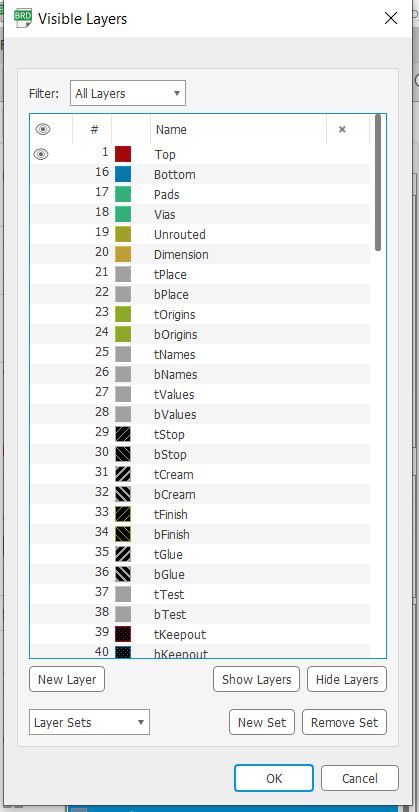
Time to export. But first I had to "clean" the board going to Layer section and hidding all part except Top Layer.
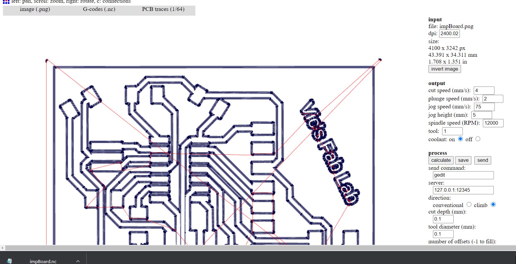
Finally, I exported using 2400 px as a parameter because it makes the image more defined and is easier for modules to check the wire and create the G-Code.
Using Fab Modules to create the G-Code. I used the parameters from the Week04 because I use dthe same machine. RPM as 12 000, tool diameter as 0.1 mm, and number of offset as 6.
Improving my Design: Ultimate Board
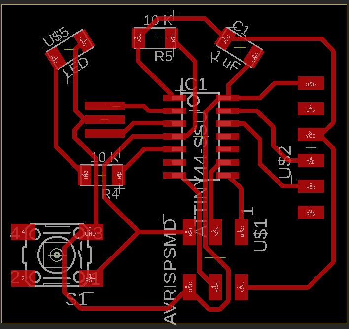
I improved my design because I wanted to use more than a single led so I added 2 more leds, and changed the functionality of the button which I previously set as a reset button.
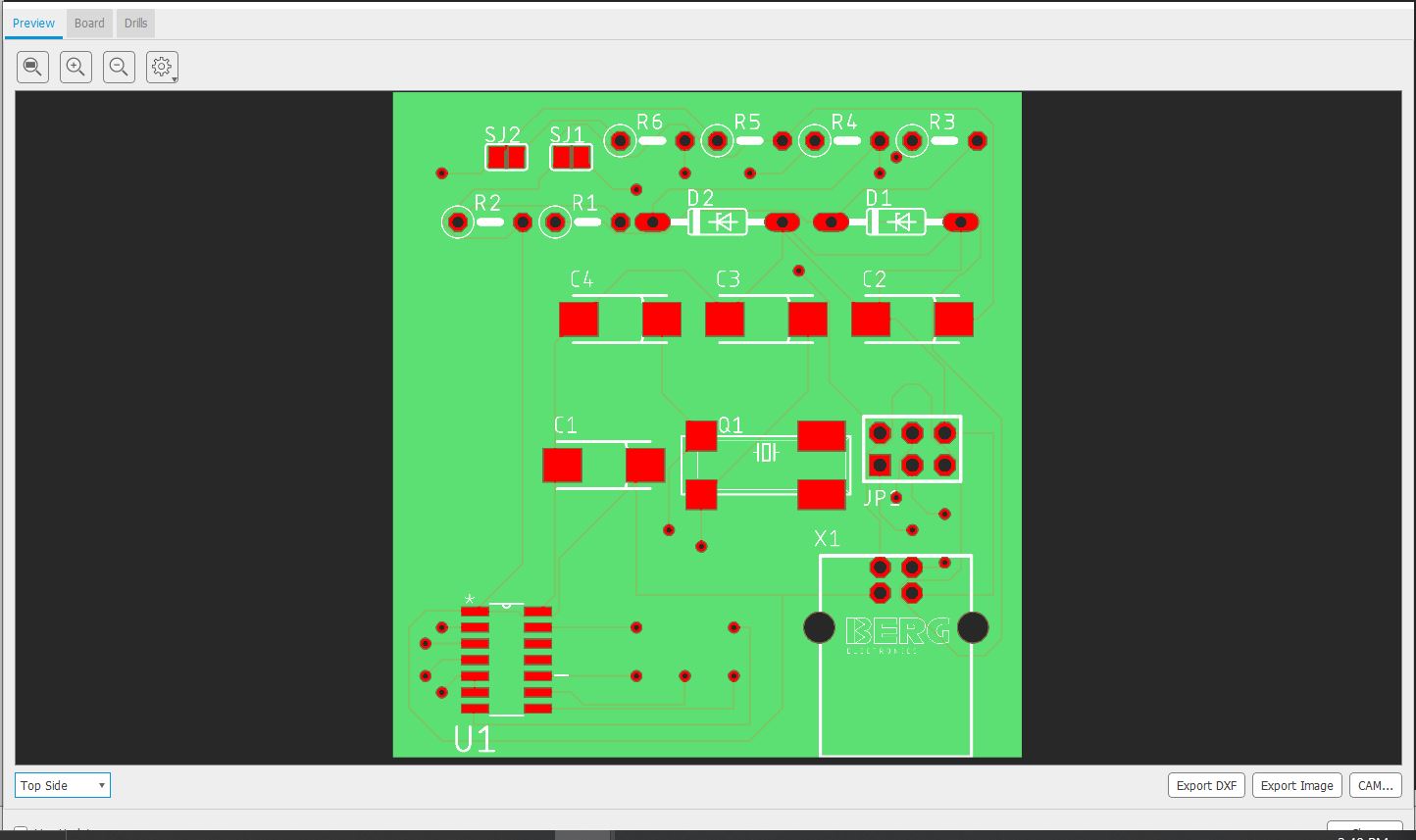
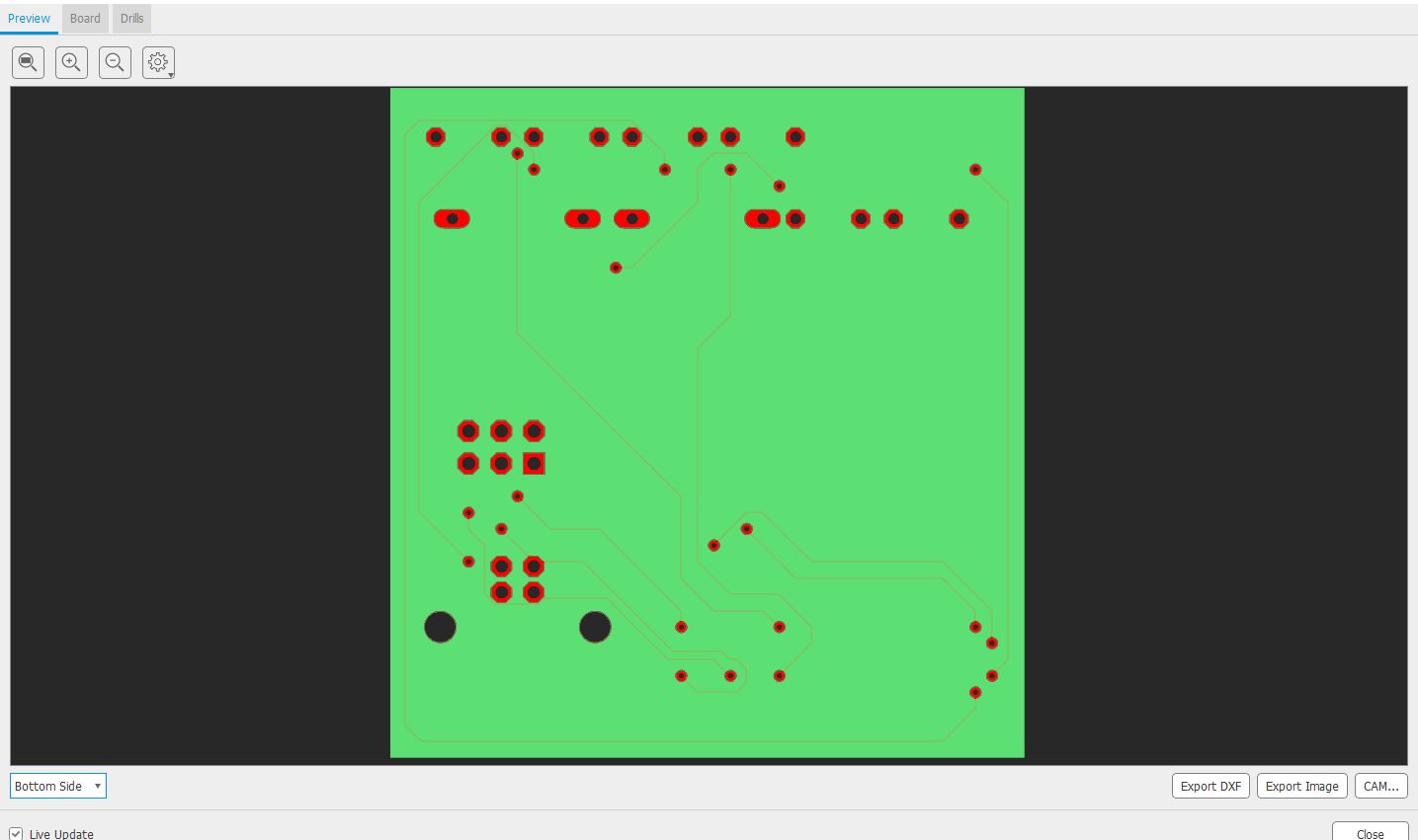
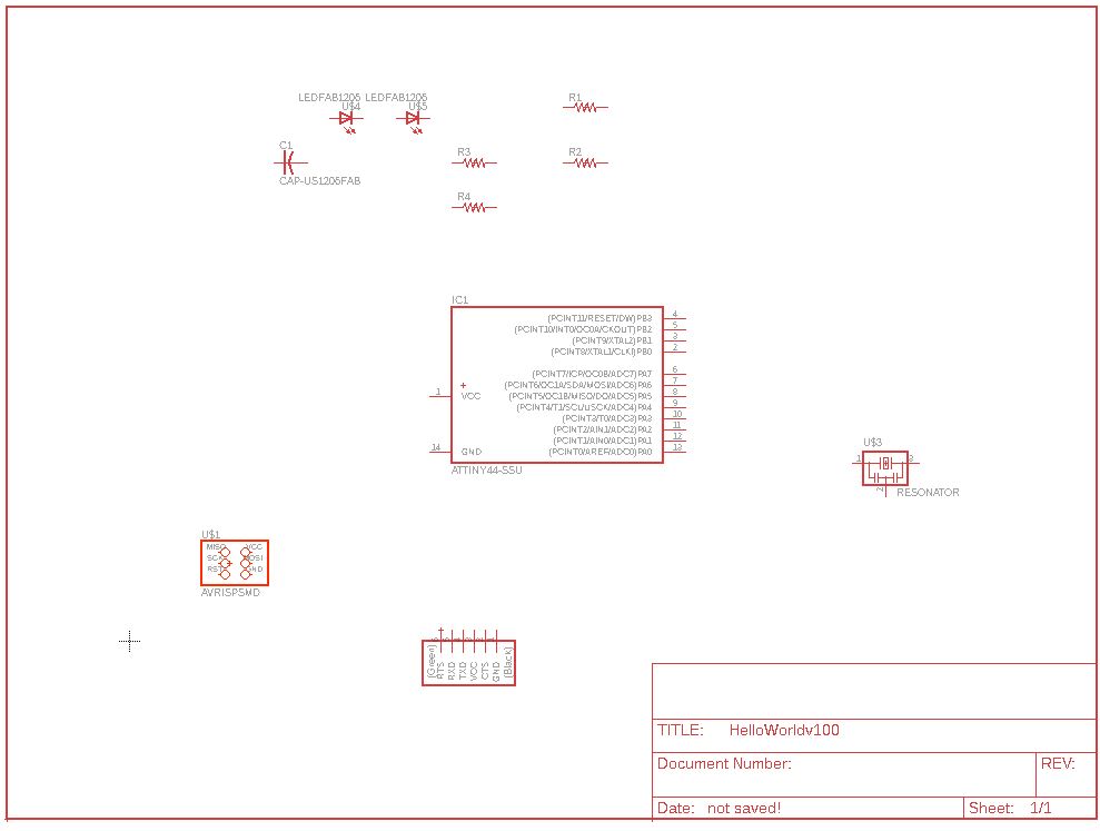
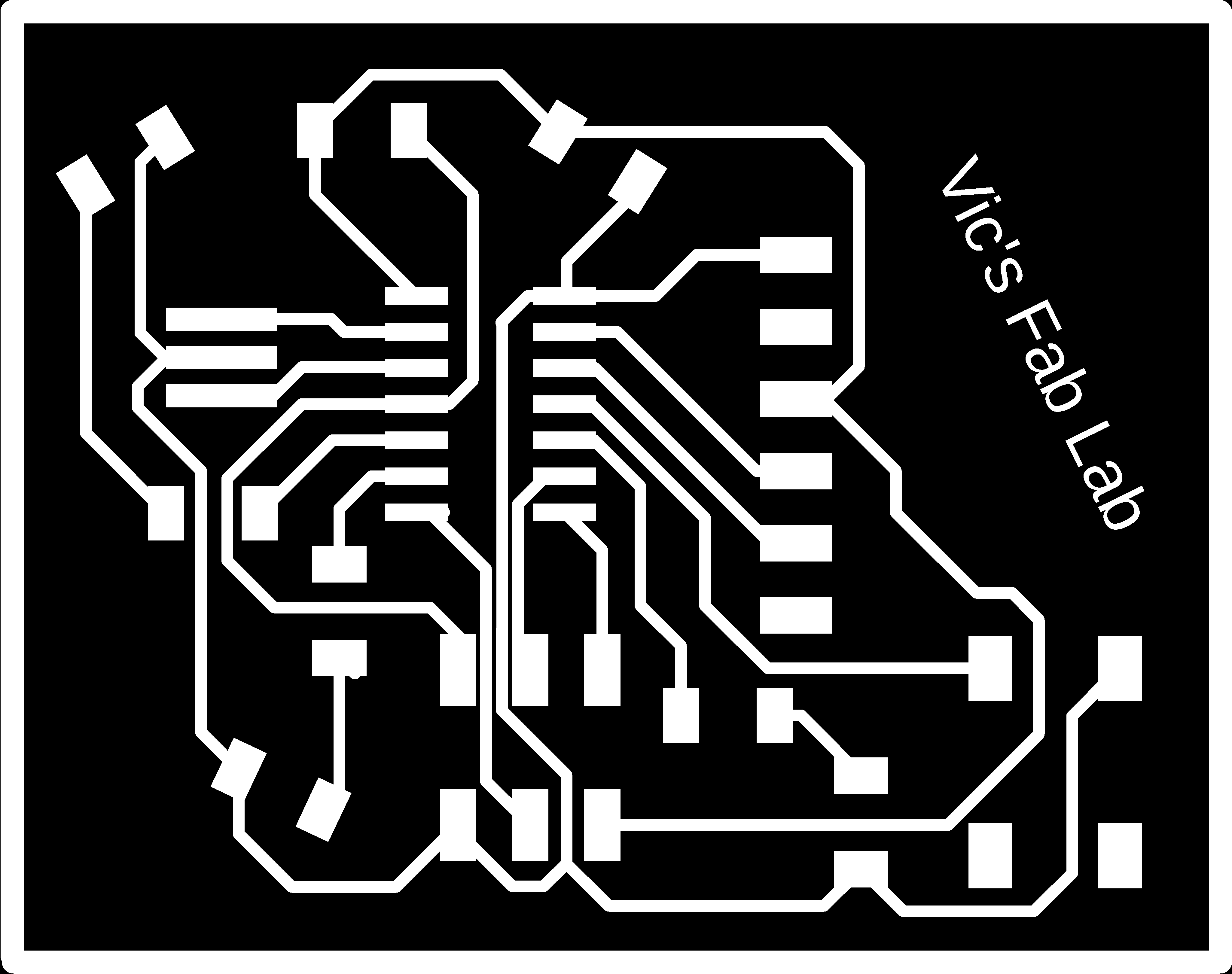
Here is my new design, 1st the schematic and 2nd the board distribution.
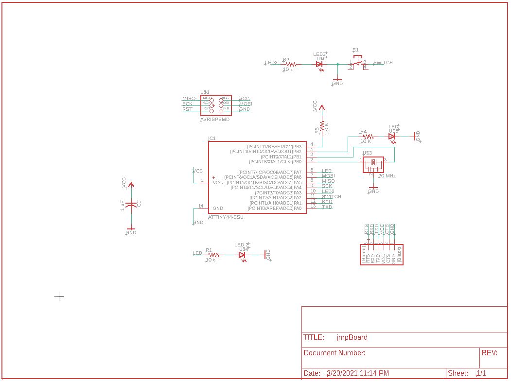
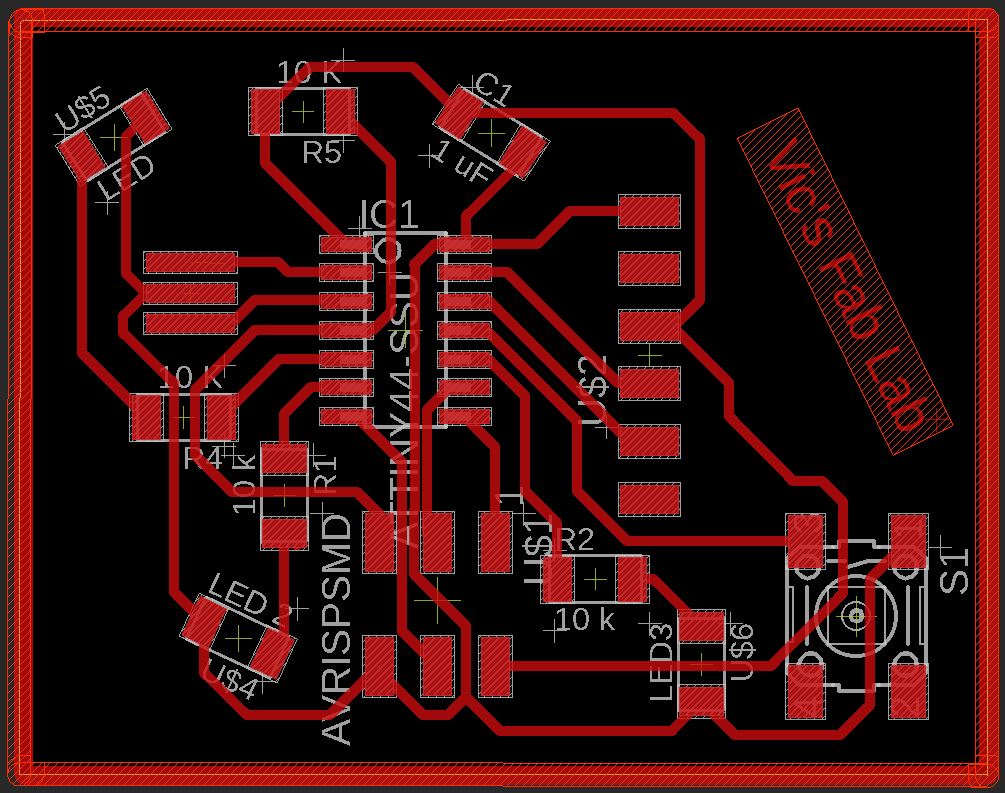
As you can see at first picture, leds have similar symbol as Diodes, additional how they are configurated they need a resistor.
Then following the process we learnt at Week Fourth: Electronic Production I generated the G-Code.
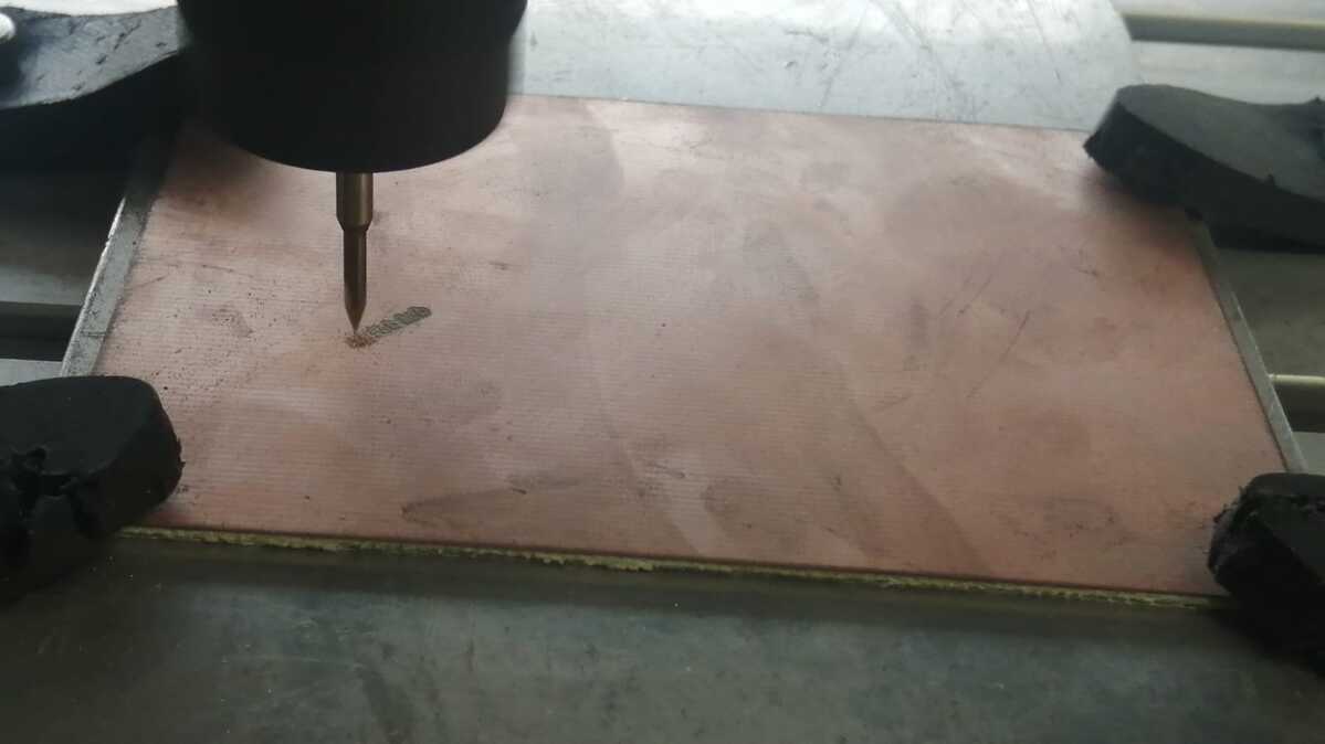
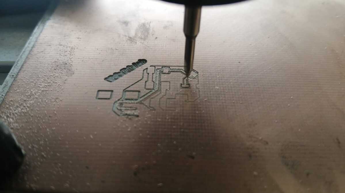
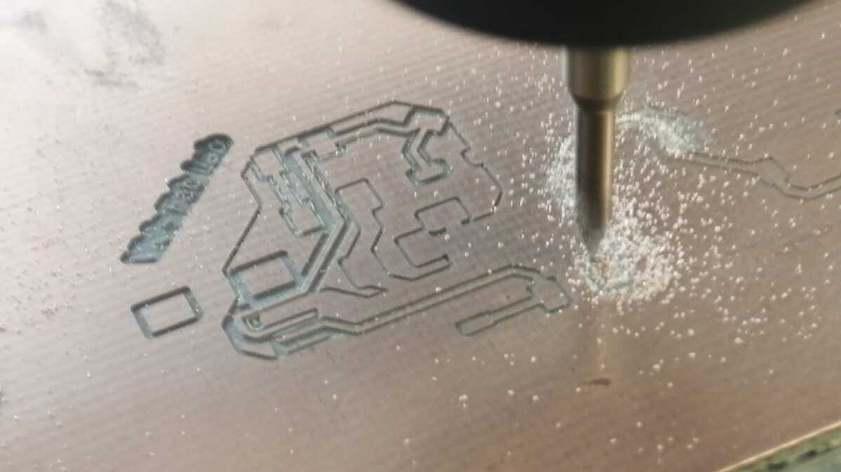
At that week assignment we learnt how to operate the Roland machine to completed the production. Here are some pictures of the milling process.
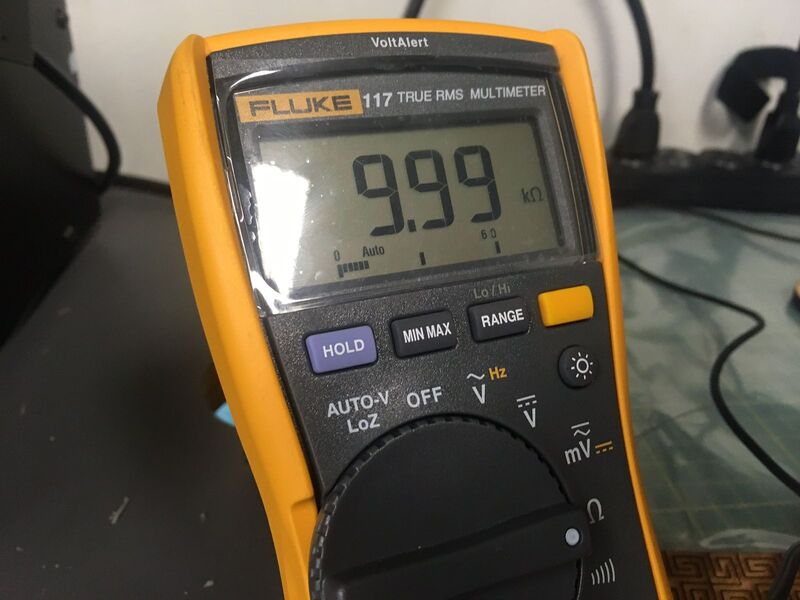
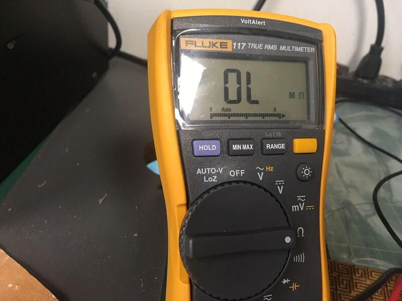
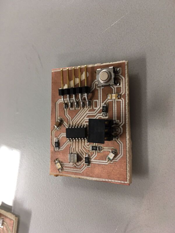
Now was time to solder the components, which I had to check the capacity of them with a
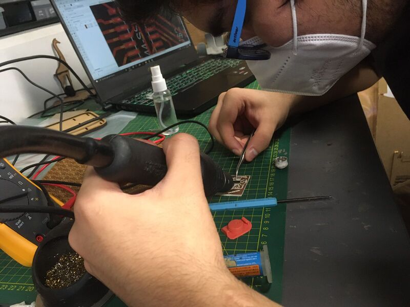
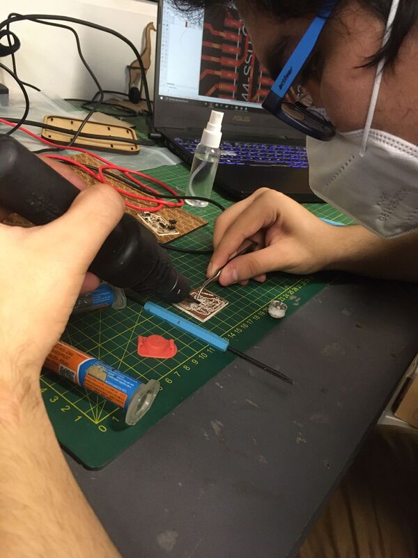
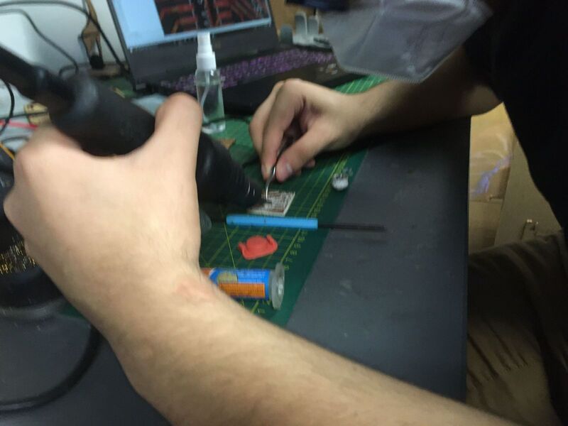
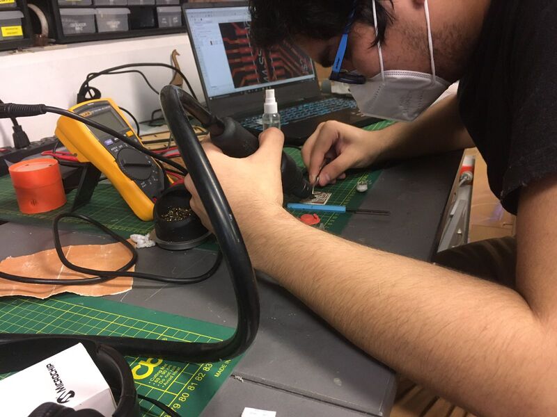
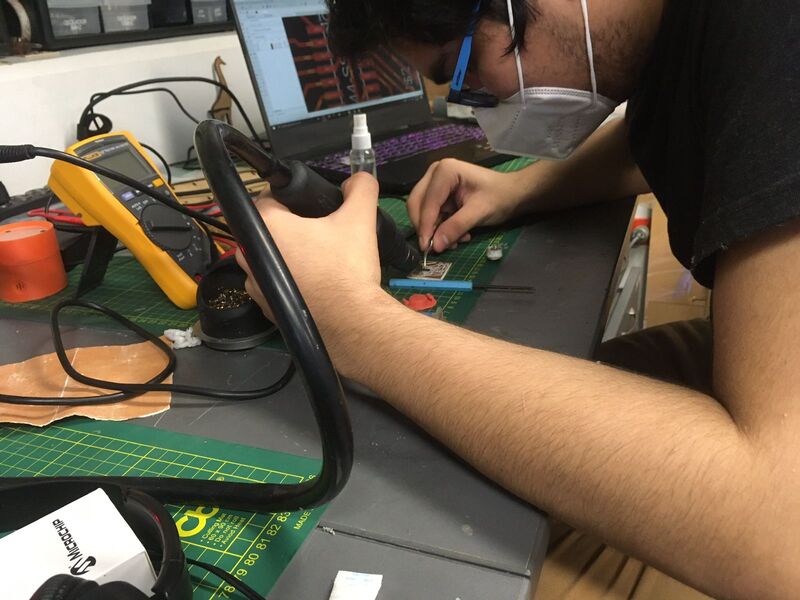
Note: As you can see I was wearing the same clothes as Electronic Production assignment. It was because at the pandemic situation I had some work accumulated so I solder my ISP and this board at the same day.
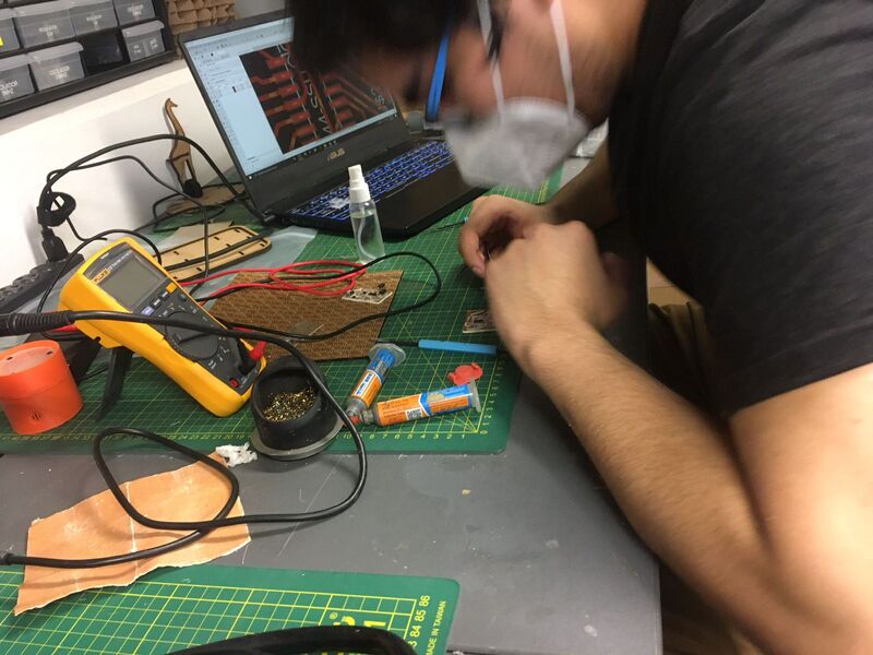
Finally having this beautiful board that I made.

Testing
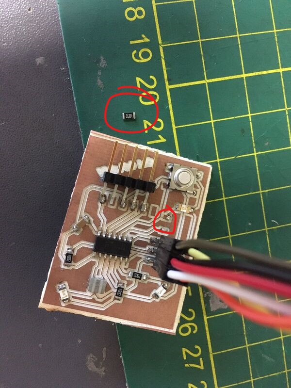
Now, is time to test this board for what I used Arduino IDE to program and test it.Oops, there was a problem. 1 of my 3 leds didn't blink as you can see.
I asked for some help to my supervisor to identify where would be the problem. He showed me that I had badly soldered a resistor as you can see now.