5. Electronics production
This week I worked on:
- Learning about PCB
- Learning how to Design a PCB
- Making an in-circuit programmer
- Soldering Electronics
- Tested my in-circuit programmer
- Group Assignment
Learning about PCB (Print-Circuit Board)
This was the first time I ever heard about PCB (Printed Circuit Board). That said, I was not sure what that was. I was able to get an good understanding of what a PCB is and what it does through Adafruit’s Circuit Playground, specifically their Circuit Playground - P is for PCB video. Additionally, I was able to learn more about PCBs through What are PCBs || How do PCBs Work?.
That said, PCBs as the foundational building block of most modern electronic devices. PCBs allows signals and power to be routed between physical devices. By soldering metals, we can make electrical connections between the surface of the PCB and the electronic components.
Once I learned what a PCB was, it was time to learn how to design a PCB.
Learning how to Design a PCB
I navigated to LinkedIn Learning to learn how to design PCB with EAGLE.
The Learning PCB Design with EAGLE with Taylor Hokanson is a 1 hour and 15 minutes course that teaches individuals how to prepare electronic schematics for fabrication as printed circuit boards (PCBs) using the EAGLE PCB layout software from Autodesk.
Making an in-circuit programmer w/ help
I was told that this week assignment was much simplier than I thought and I can used a previous design like the following:
to replicate a PCB programmer link the one below:
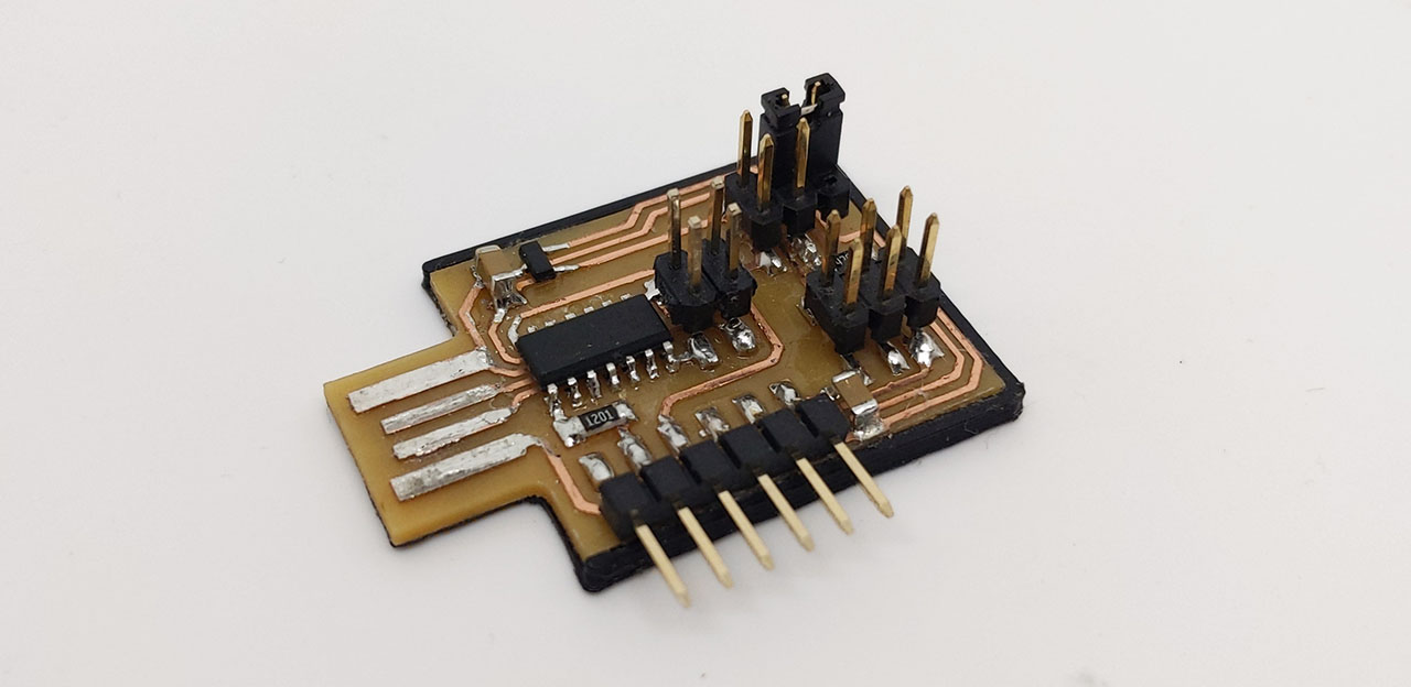
With the help of my instructor, Spencer Mewherter, and team member, Xiaolin (Linda) Zhen, we were able to create a PCB.
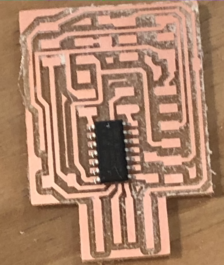
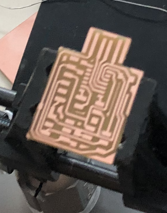
Minimal but effective. The process to create the above or a similar PCB was simple. We used the Trace.png file which created the lines (the traces) on the PCB for the electricity to travel. I like to think of the Traces as a path for the electricity. The Interior file created the cutout of the PCB.
Now, in order to get the Trace and Interior to be placed on Copper, we needed to use the MonoFab SRM-20, the milling machine.
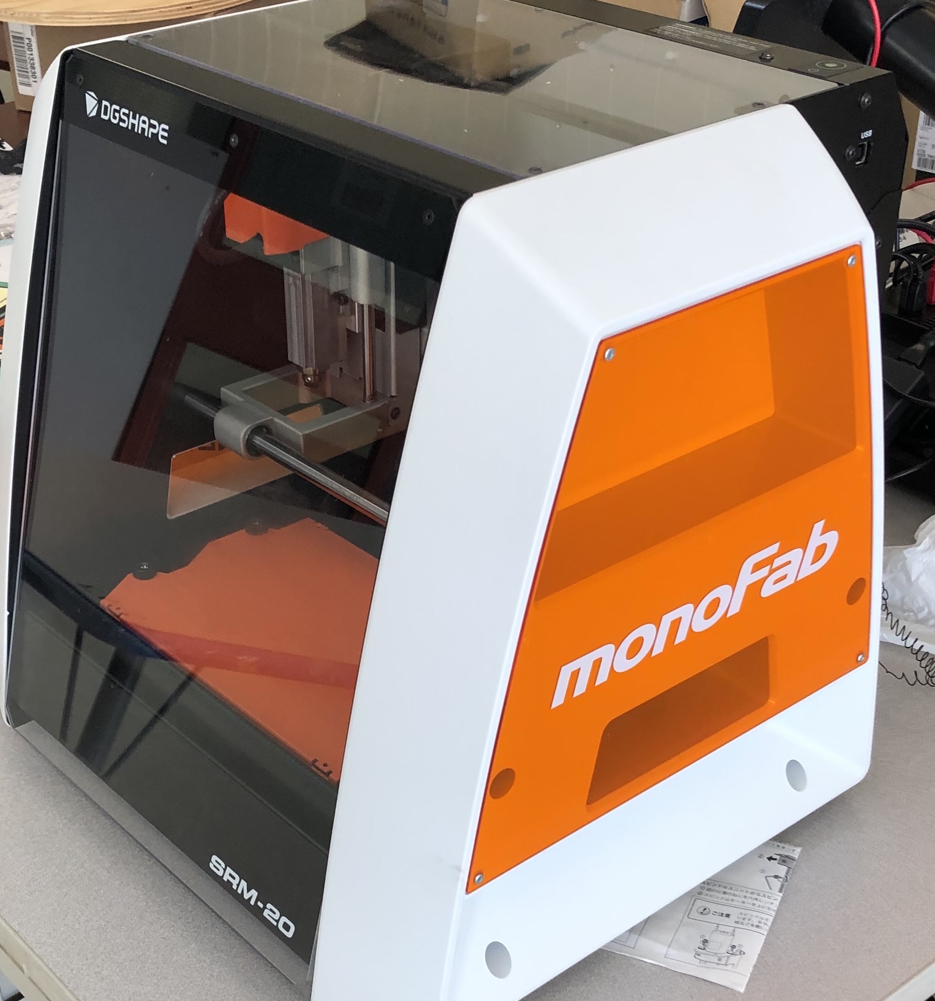
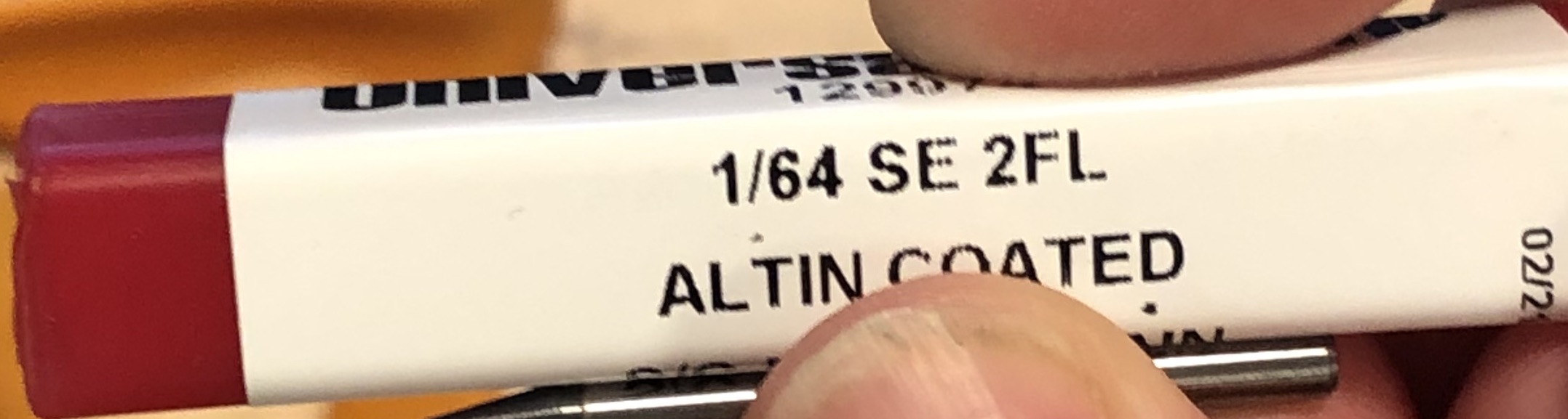
The machine was not difficult to use. We started with the Traces as it is best practice to do so. We used a 1/64 SE 2FL Altin Coated miling pin to mill the traces.
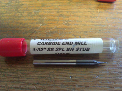
Once finished with the Traces, we changed the mill to a 1/32 SE 2FL Altin Coated mill for the Interior cut.
The result came out okay as the mills were worn out. However, this made for a good practice.
Soldering Electronics
Once we were finished with miling, we moved onto soldering the electronics. Soldering the electronics consisted of us using a soldering station with a soldering iron to melt lead onto our PCB. Melting lead onto the PCB allowed us to attach each component to the PCB. With the components attached to the PCB, we can program the PCB.
To get started, we set up the environment to begin soldering.
The soldering process takes time and patience but, it is quite peaceful. With enough practice, it becomes easier. Prior to soldering, I was able to watch a LinkedIn Learning about best practices and tools for Soldering. , with enought practice, it does get easier. Watching the LinkedIn Learning course on Soldering electronics did provide a few techniques to have a clean result - Learning Soldering for Electronics.
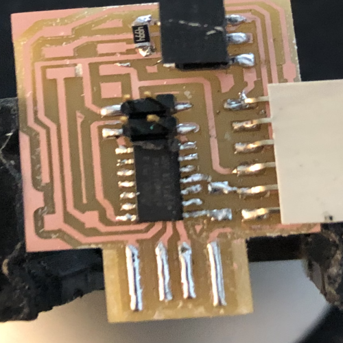
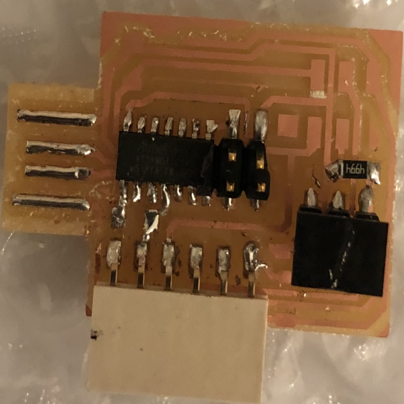
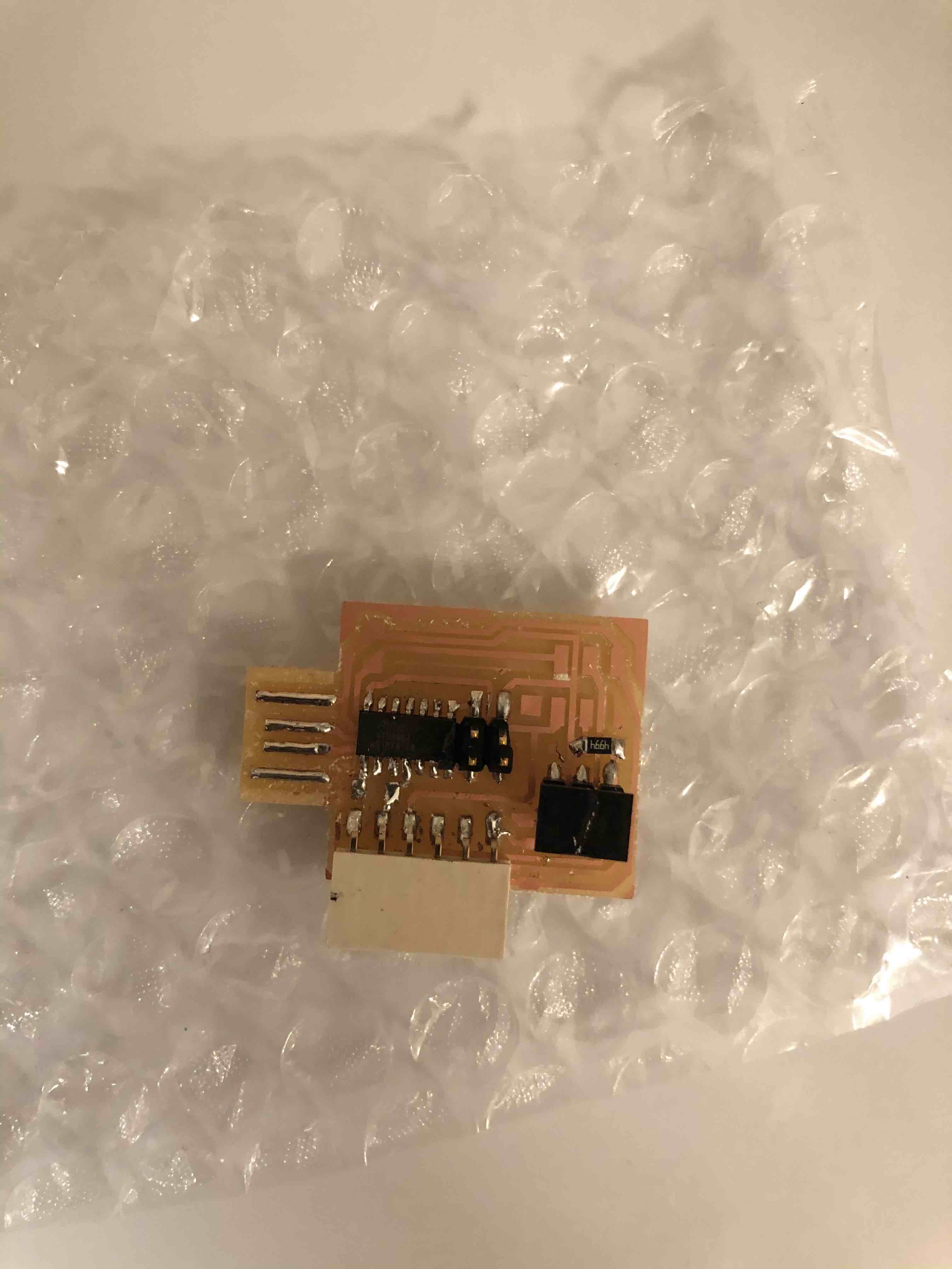
The above PCBs was created with the help of Xiaolin (Linda) Zhen.
As mentioned, this above board was good practice in making an in-circuit PCB board. I want to re-make the in-circuit PCB board as I felt the Traces were not as clean as I would like them to be.
Testing the Programmer PCB
I was able to test the PCB board by performing a burn-in. A burn-in is the testing of a PCB to detect early failures and establish load capacity. This is often done by running a power supply and firmware through the electronics for some time.
I connected the PCB to my computer via USB for some time:
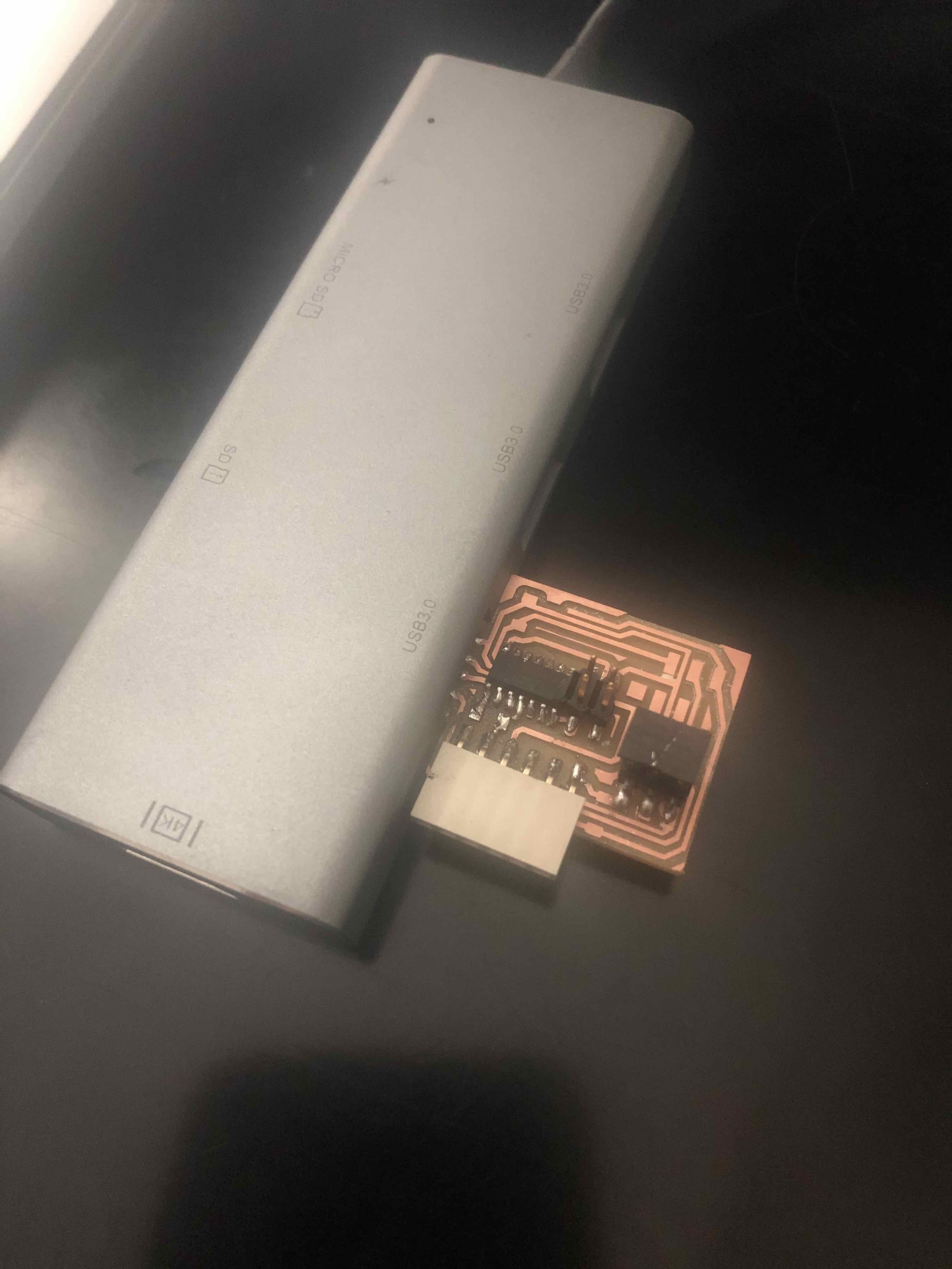
No smoking occured while it was being plugged into the computer. I concluded that the burn-in test passed and the integrated PCB can be used.
Group Assignment
This week group assignment was to characterize the design rules for the team PCB production. But our team did not participate in this week group assignment. Group’s Page