
This week, we hat to make an in-circuit-programmer by milling and stuffing a PCB..
For designing and routing of my PCB I started with this instruction for the FabTinyISP.
As I didn't want to copy this instruction entirely, I used the provided schematics to design my own PCB in KiCad.
For that I created a new project in KiCad and redraw the schematics, using the parts I had in our FabLab.
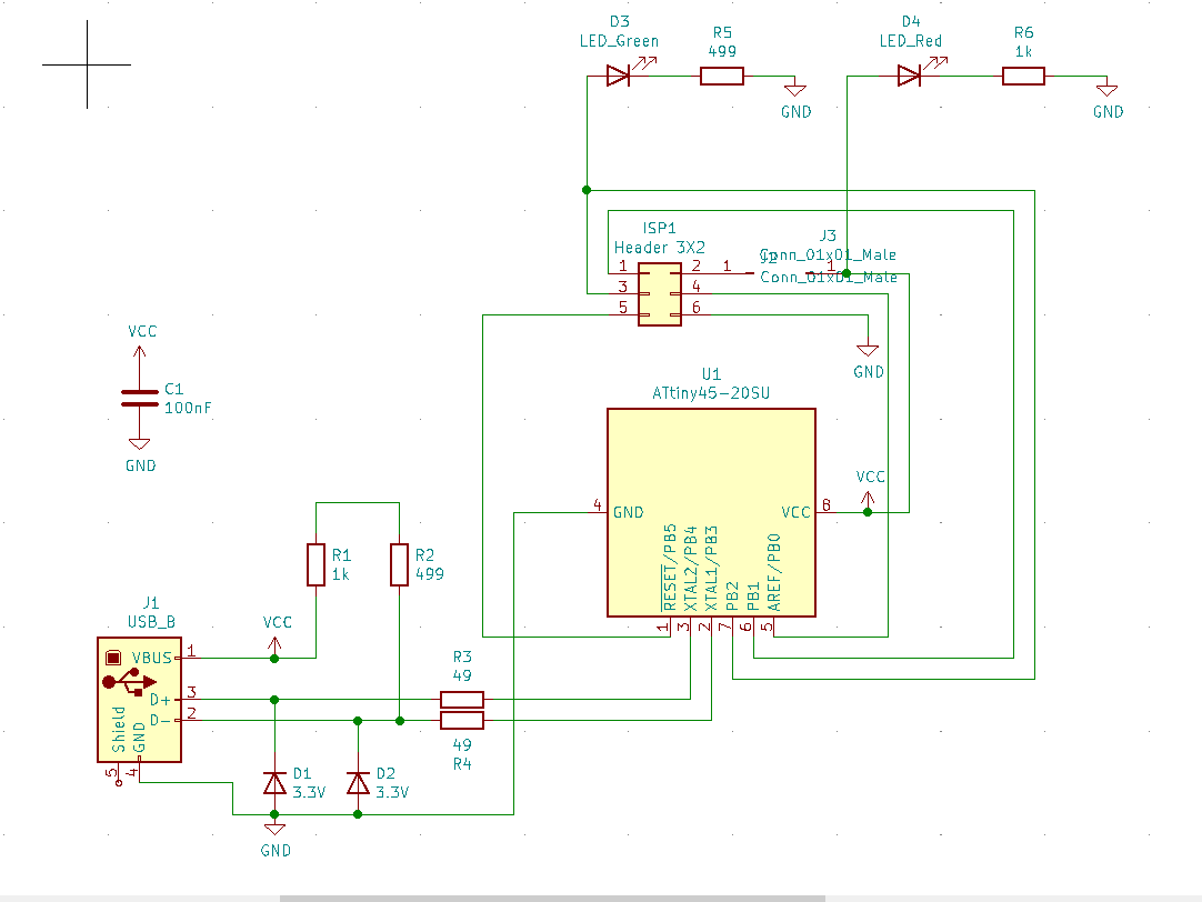
Then I inserted the foodprints for the corresponding parts and create a new layout by routing all the connections.
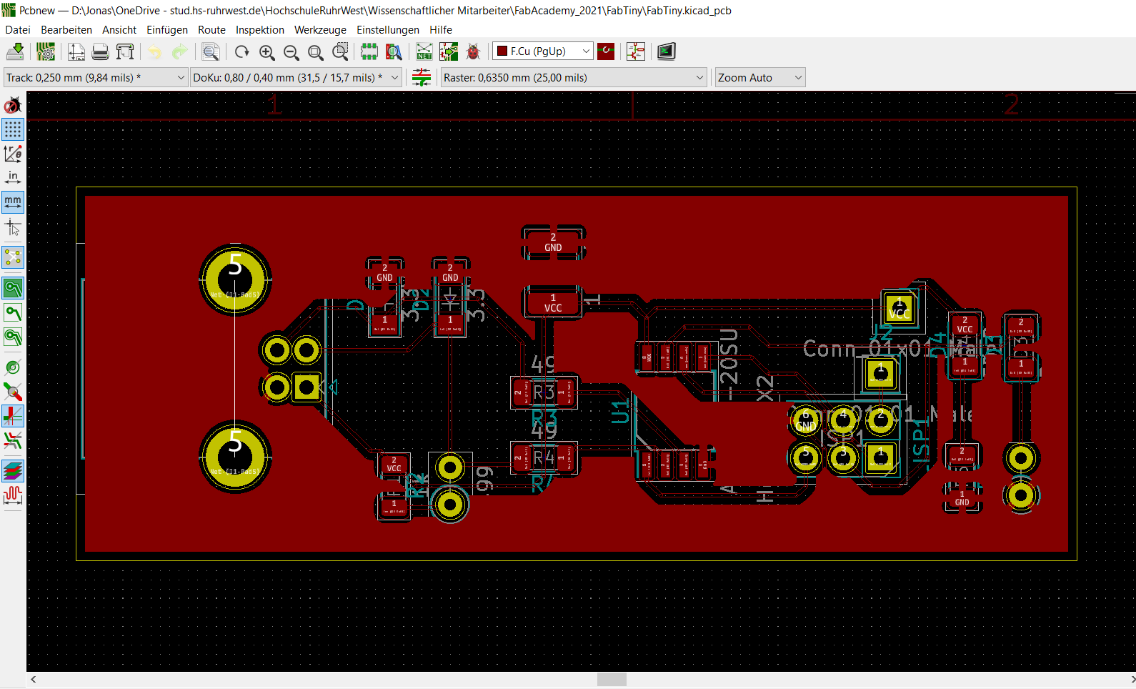
At the end I exportet the design in gerber-format.
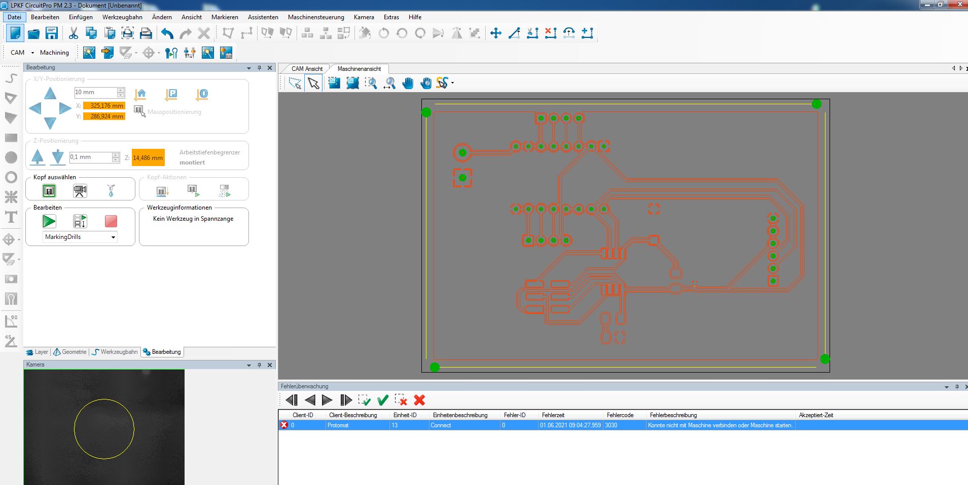
In our FabLab we use a LPKF - pcb milling machine. For that I importet my pcb design as gerber-format, the milling machine does the rest automaticly.
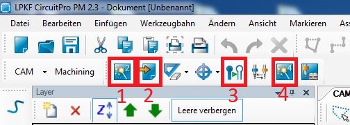
In the following images I will show you step by step, what settings you have to set:
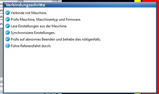
First you have to let the software connect to the machine:
Then we go from Step 1 to 4:
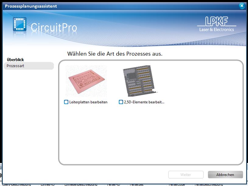
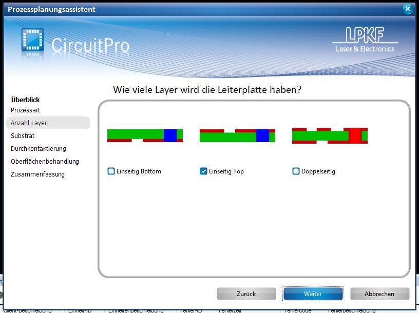
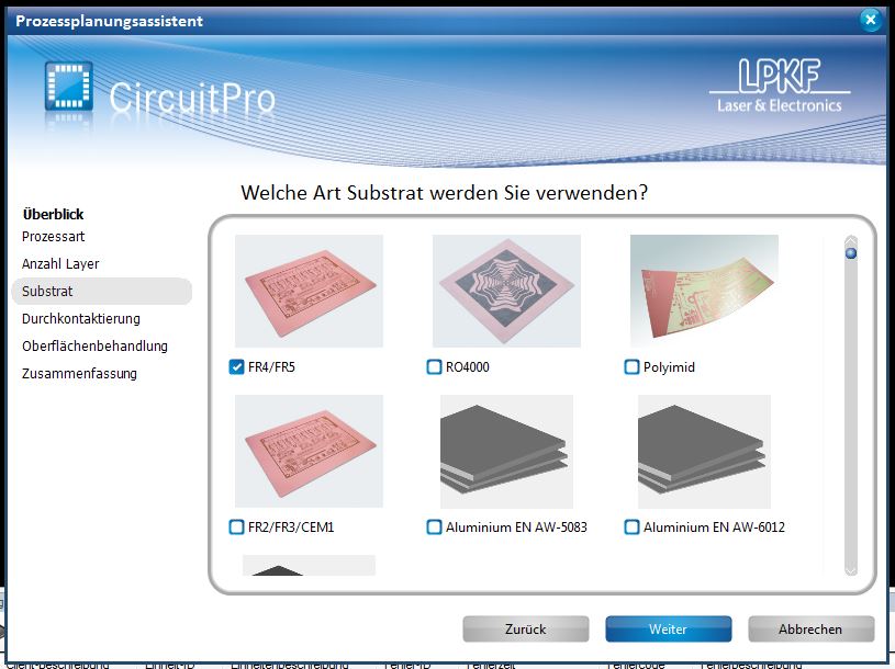
At Step 1 we set up the material we use:
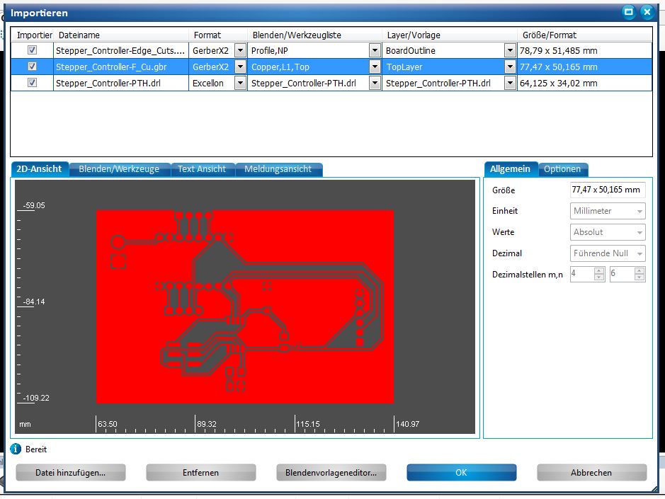
At Step 2 we import our gerber files:
At Step 3 we let the programm generate the path for milling and cutting the PCB:
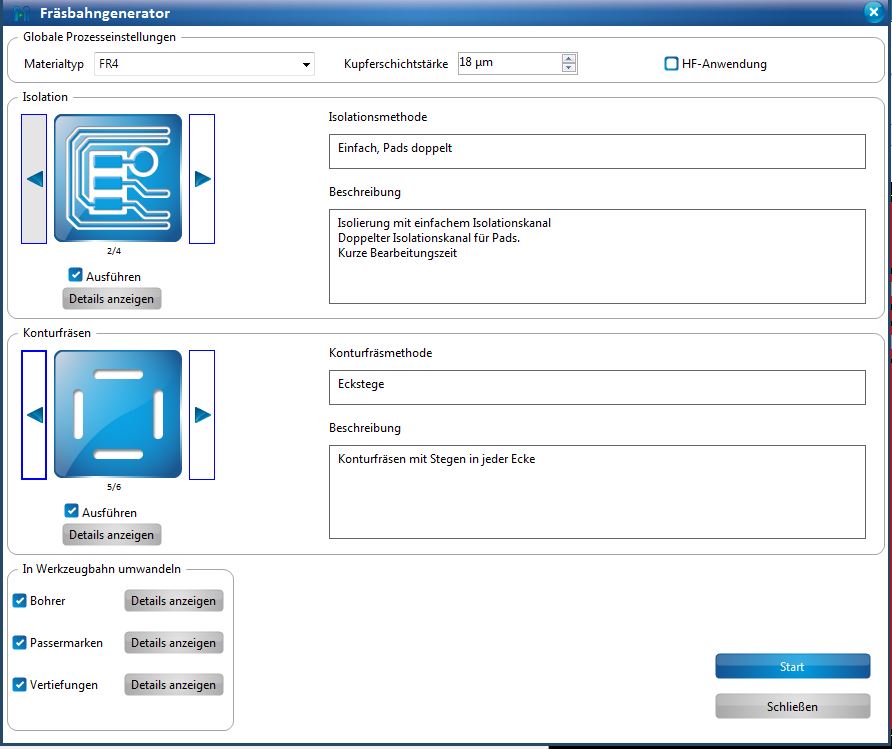
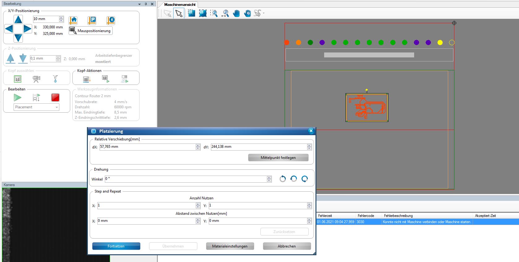
At the last Step we place our generated PCD-path relative to the copper-board in the machine, then we start the job:
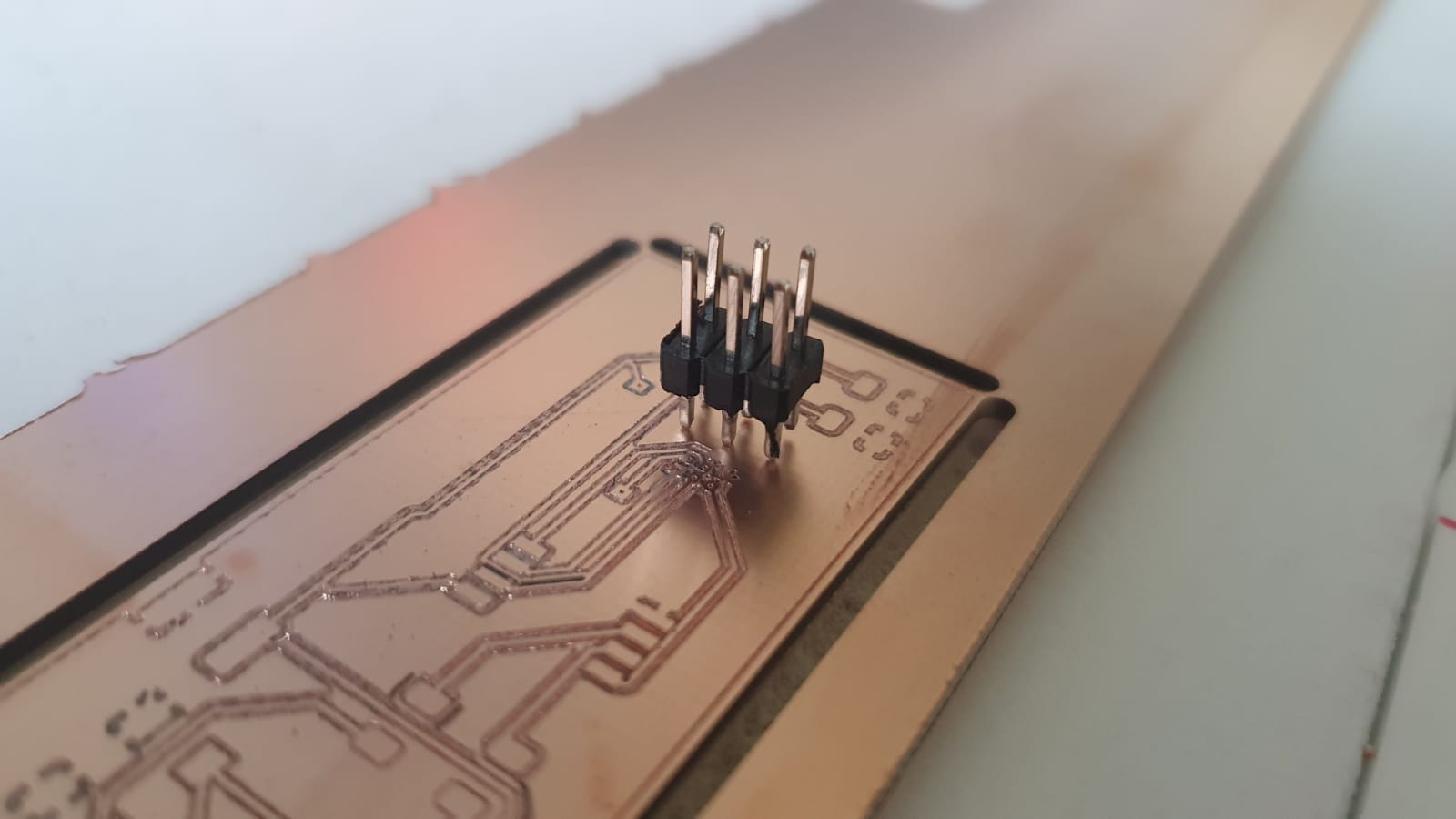
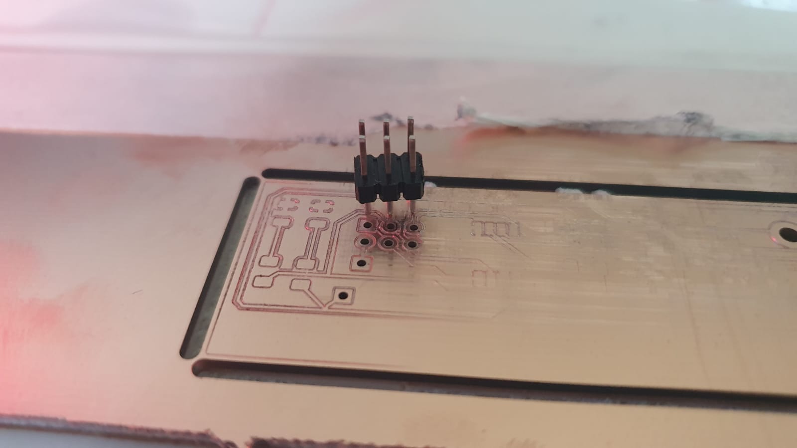
In my first design I had set the wrong foodprint for the 6 pin header, as you can see in this image:
So I changed the foodprint in KiCad and cutted a new PCB:
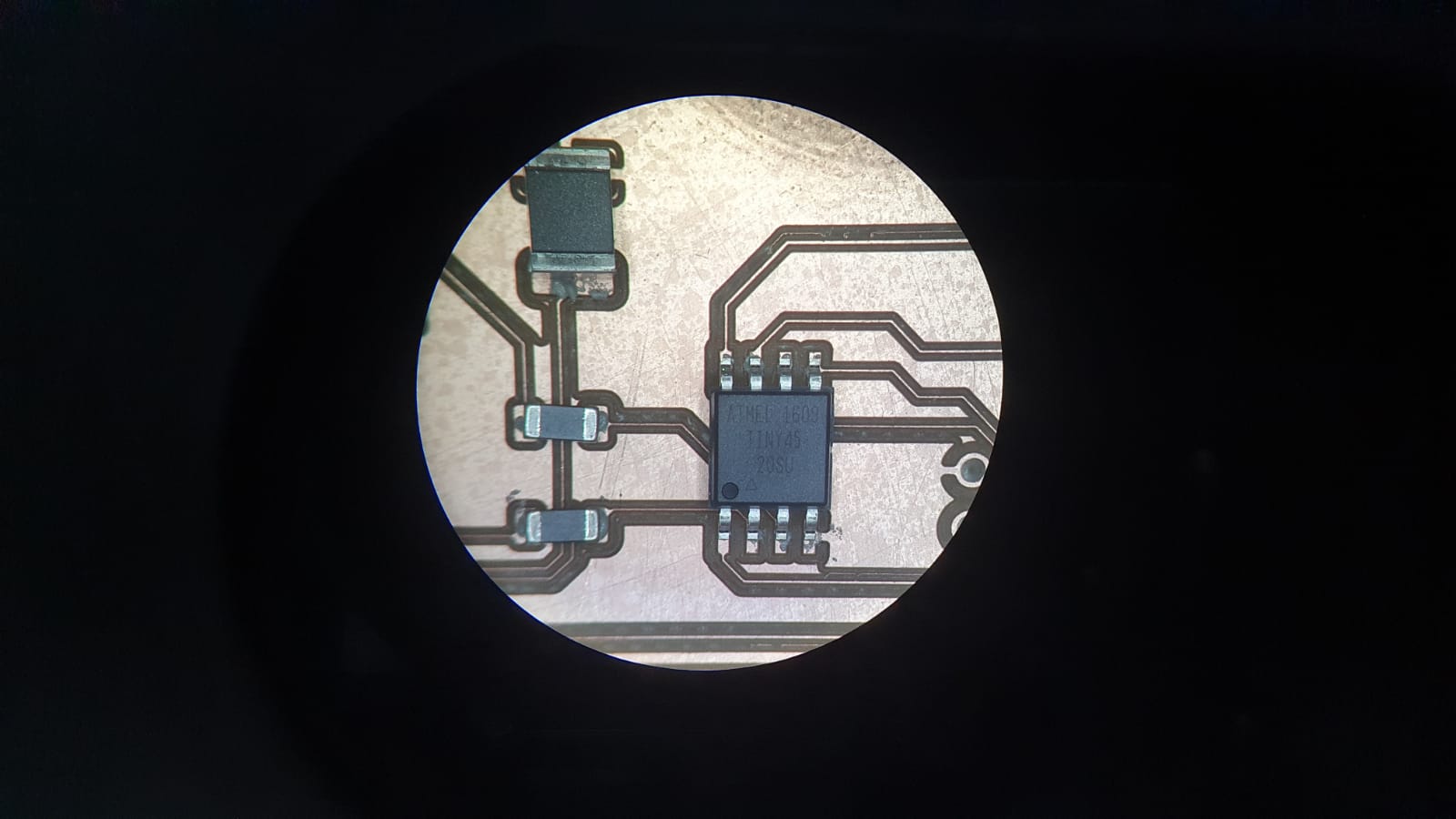
After that I put solder paste onto my pcb and placed the components. Before I put it into the ofen I viewed my parts in our microscope:
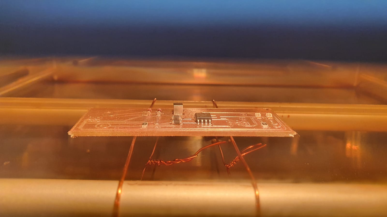
As I was satisfied I put my pcb into our heater ofen and melted the soldering paste, so that my components got soldert to my pcb:
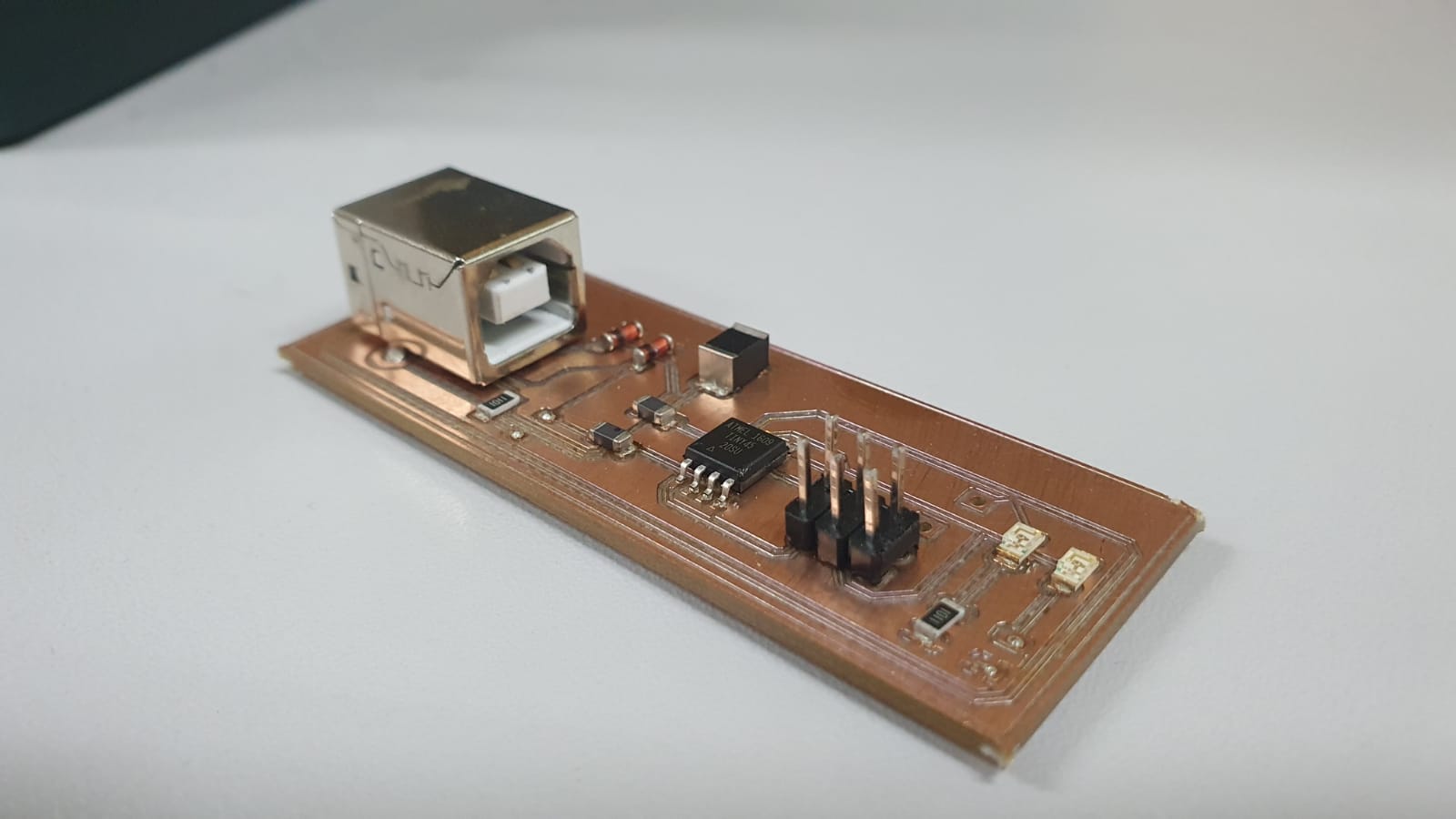
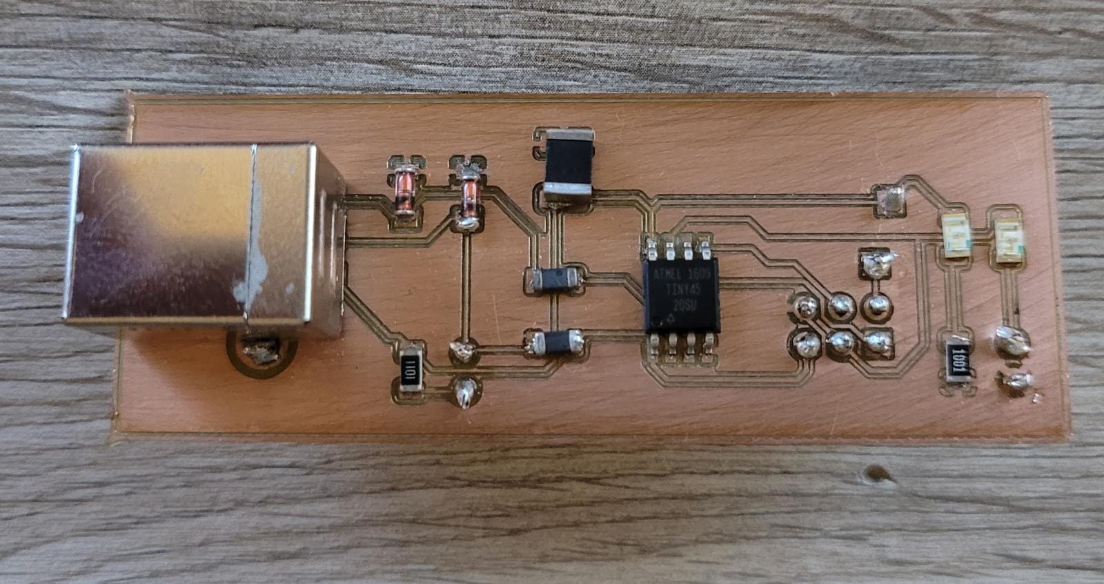
Here you can see my finsihed PCB!
Yes I know, my USB Header is mounted the wrong way arround, I will fix this the next time i can visit our FabLab :D
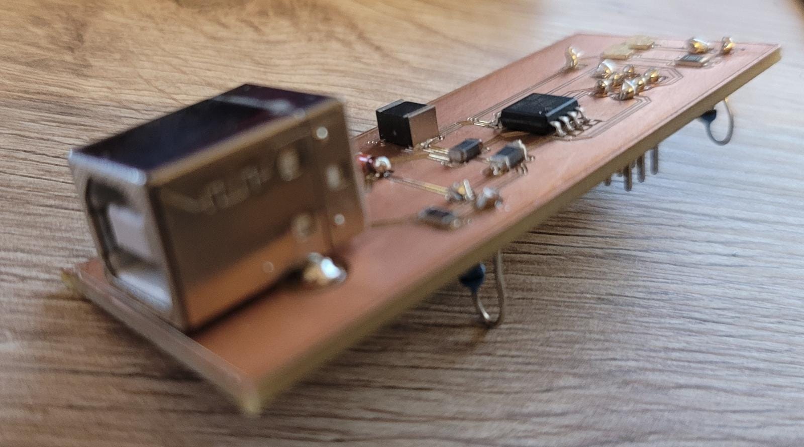
So after I changed my design in KiCad I milled a new PCB, this time with the USB Port in right orientiation, desoldered my components from the old board and re-soldered it to the new board:
As you will see I located the ISP-Header under my PCB, just for make the soldering a little bit easier:
So after I checked my board for shorts I followed this tutorial for flashing the turorial.
I downloaded the firmware HERE and extracted the files. I the opened Git Bash and navigated into the directory.
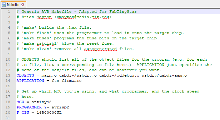
With the "make"-command I build the hex file which will be the firmware for the FabTinyISP:
I edited the Makefile according to the programmer I used, in my case a AVRISP2, in line 19:
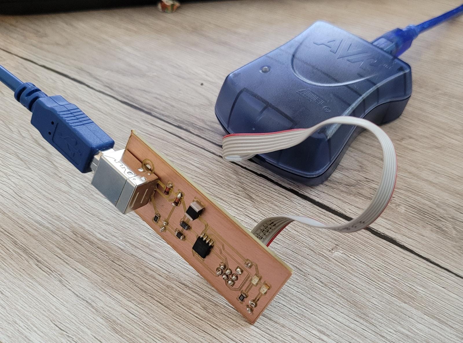
After that I connected the USB-cable and the programmer to my FabTinyISP, which looked like this:
First I used "make flash" to flash the firmware:
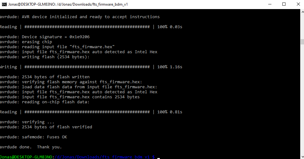
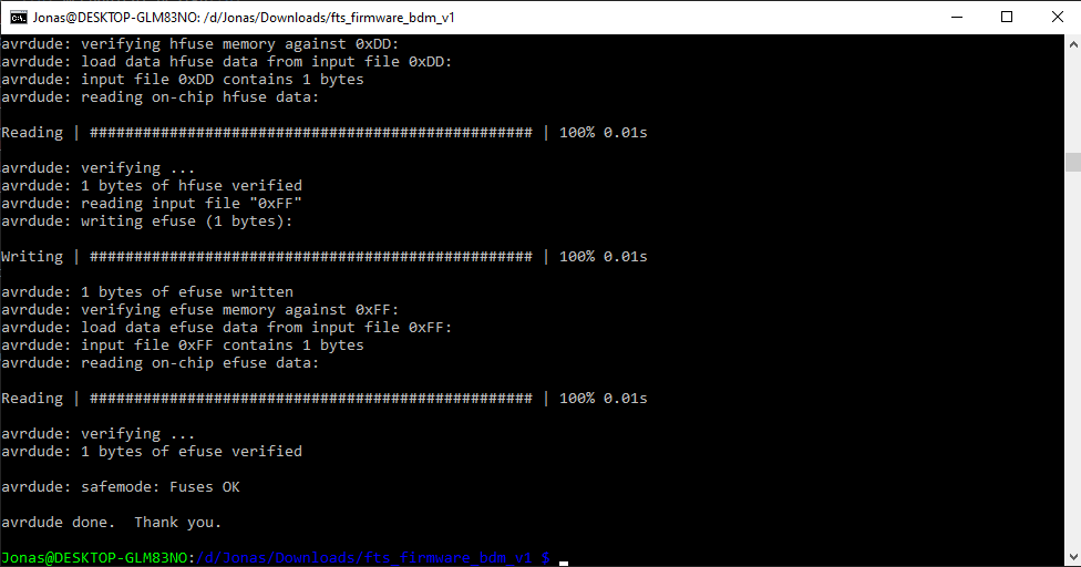
Then I set the clock fuse via "make fuses":
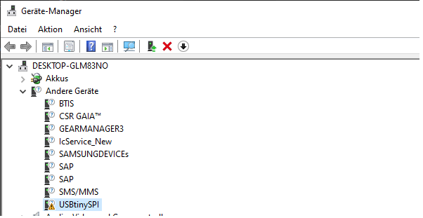
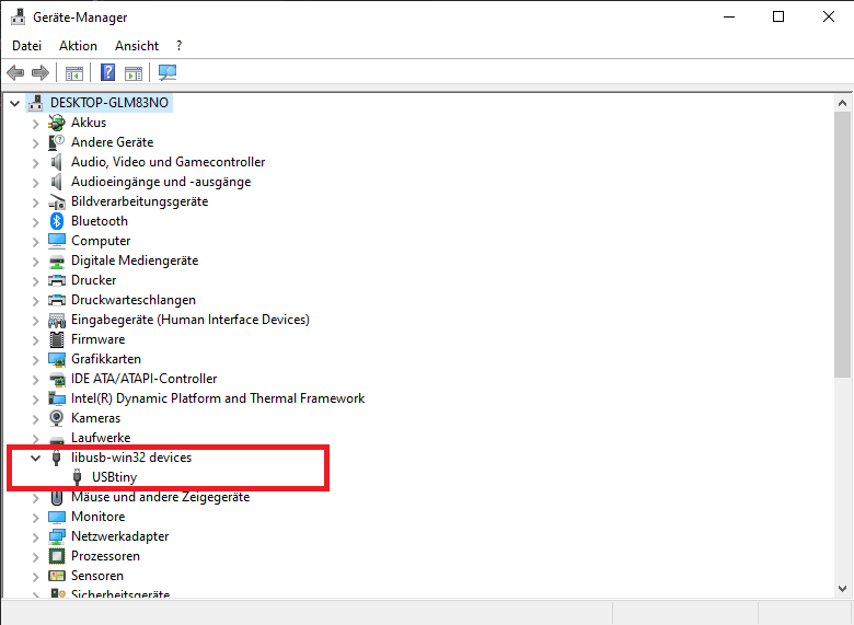
I checked that my computer lists the FabTinyISP in the device manager:
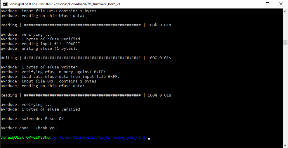
Then I disabled the fuse pin via "make rstdisbl":
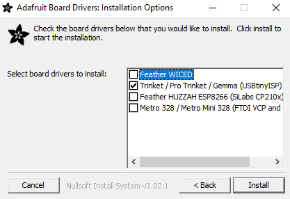
At the end I installed the needet driver and looked at my device manager again, confirming that my FabTinyISP is listes as it should:
It worked!!
As group assignment we had to characterize the design rules for our PCB production.
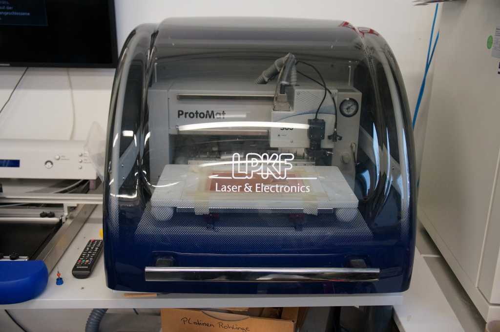
In our FabLab we have a LPKF ProtoMat S63 with following specs:
| Quick Specs | |
|---|---|
| workspace | 229mm x 305mm x 35/22mm |
| automated tools | 15 |
| milling and drilling spindle | 60.000 rpm |
| precision | 100 µm |
| special functions | changes the tools automaticly |