6. Electronics design
This week we had to design our own printed curcuit board. I have ATtiny85 in the lab so I decided to use it. As for the software to make the pcb I used KiCad. I loaded the fab library in KiCad and used the fab components. For the group assignment we had to use the test equipment in your lab to observe the operation of a microcontroller circuit board
EDA and PCB KiCad design
Electronic design automation (EDA), also referred to as electronic computer-aided design (ECAD), is a category of software tools for designing electronic systems such as integrated circuits and printed circuit boards. The tools work together in a design flow that chip designers use to design and analyze entire semiconductor chips. Since a modern semiconductor chip can have billions of components, EDA tools are essential for their design.
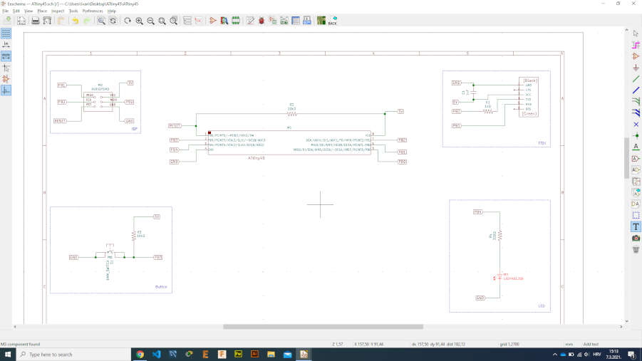
The first step was to download KiCad from here. The instructor showed us how to insert the fab library and use the fab components to create schematic and pcb. I followed this tutorial. I went to file -> new project. I called it ATTiny45 and started making a schematic. On the right I clicked on the place symbol icon. After that, I clicked on an empty space and a selection of components appeared. Below you can see which components I used.
- Resistors: 1kΩ, 10kΩ (2 pieces) and 470Ω
- 1uF capacitor
- LED (green in my case)
- 6mm switch
- ATTiny85 Microcontroller
- ISP and FTDI header
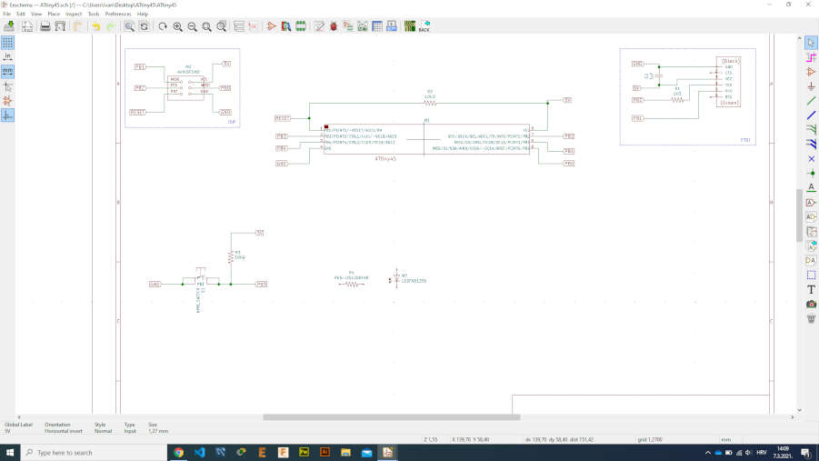
After I put it all together I decided to separate them and label them so they look like in the picture.
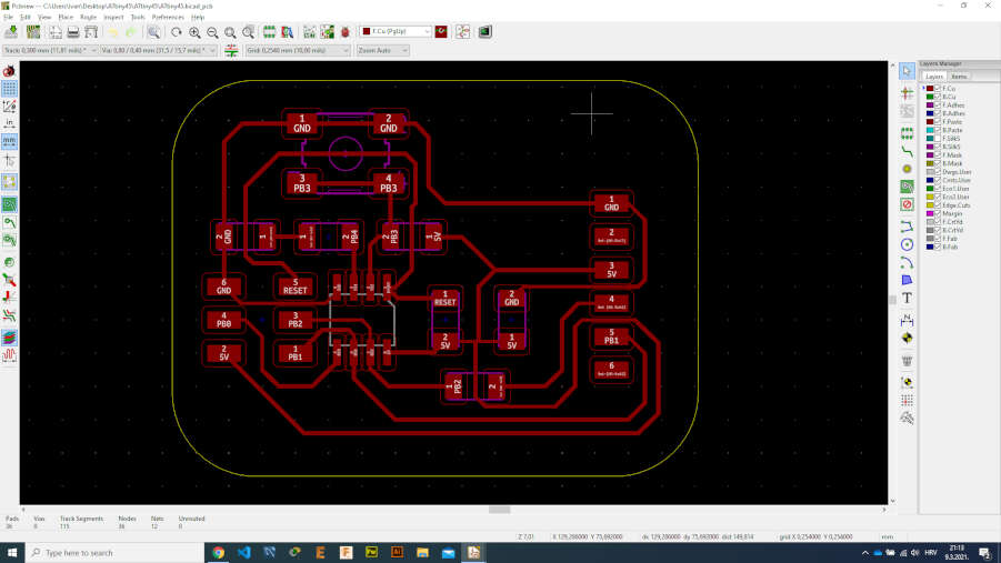
Before design PCB I clicked on the generate netlist icon to generate a list of components and saved it. I started the PCB layout editor and loaded the netlist by pressing the load netlist button. After that I choose where I want to put the components. All components are connected by a thin white line. We use the route tracks icon to connect the components.
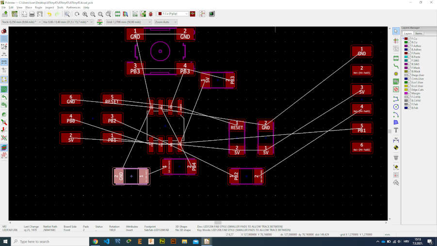
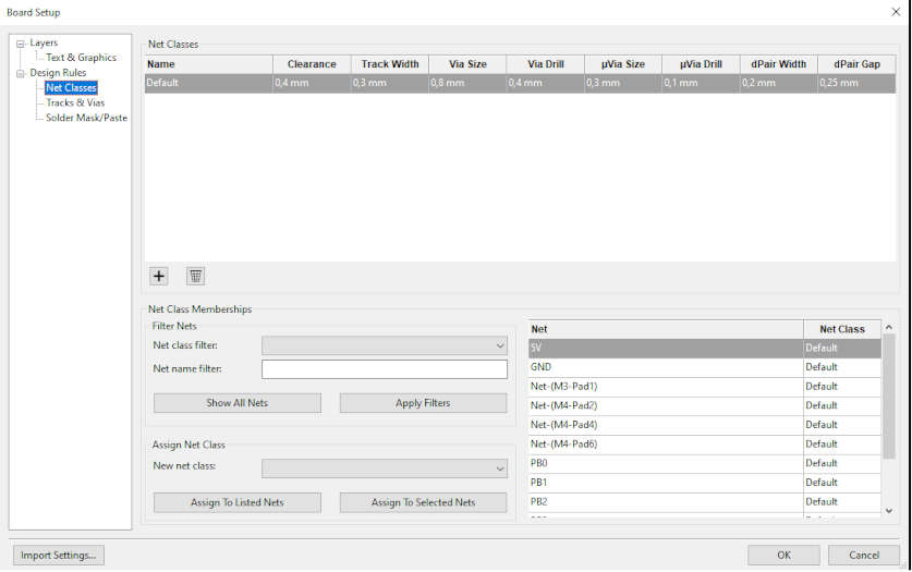
The goal with design PCB is to be able to connect everything with routes without overlapping. It took me a while to connect everything well and so the lines do not overlap. Just before drawing I went under file-> board setup. I had to set the basic parameters there. Under net classes I have placed the following:
- Clearance 0.4mm (because our end mill is 0.4mm)
- I set the track width to 0.3mm (I set 0.25mm manually somewhere)
- Other settings I left default
When I have connected everything, I click on perform design rules check. A new window appears and click Run DRC. The first time I ran it I got errors, tracks too close to board edge. This is because I did not set pcb limits.
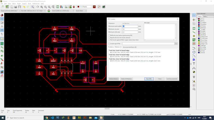
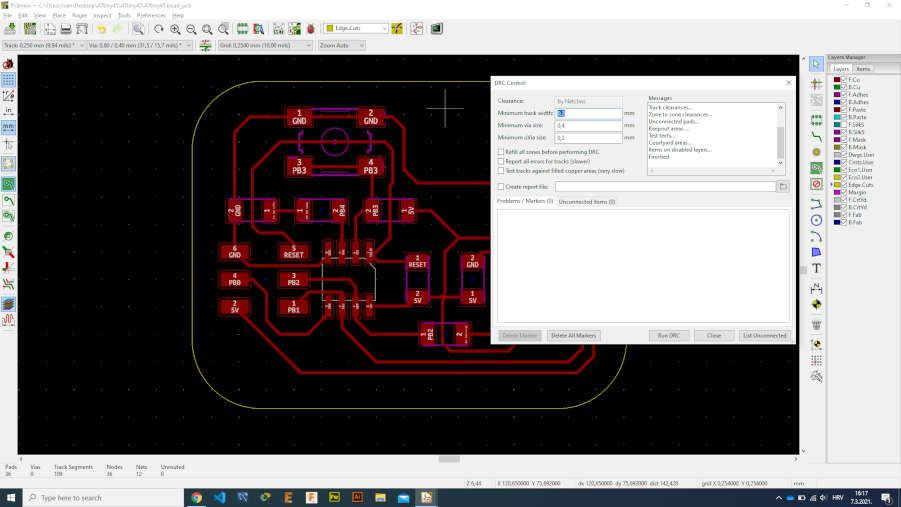
I drew the borders of the pcb by clicking on the icon add graphic line and add graphic arc. I ran the design rules check again and there were no errors.
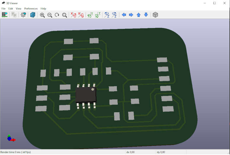
PCB bord can also be seen in 3D view by pressing ALT+3. I removed front silkscreen for better view.
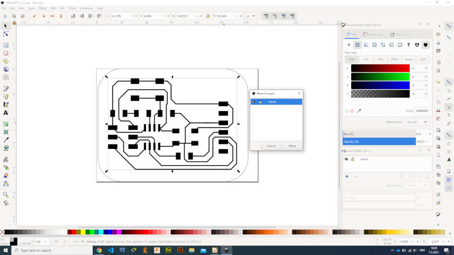
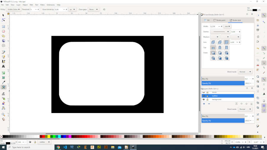
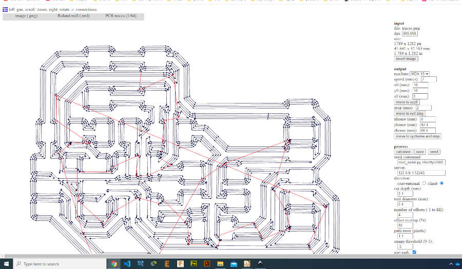
I exported pcb to svg and chose front copper layer and edge cuts layer. Fabmodules require png image to work with. To convert svg to png I used Inscape as our instructor showed us how to do that before. In Inscape I made three layers (traces, outline and background). I exported png for traces and png for outline. All pngs have 1000 dpi.
In fabmodules I uploaded traces png, and for the output I chose the rml file. For the process I chose PCB traces (1/64), for the machine I selected MDX-15 and the speed was set to 2mm / s. Then I clicked calculate and save. I did the same for outline except I changed the process from PCB traces (1/64) to PCB outline (1/32).
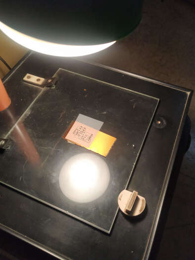
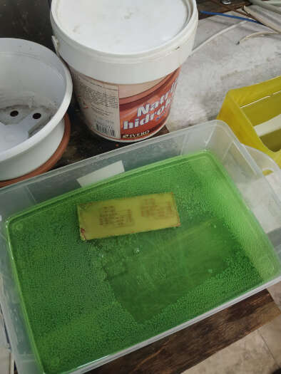
To make a PCB this time I used an etching method. After the PCB is exposed to the UV light it goes into the developer and then in a etching solution. Whole process can be seen in Electronic production week. The results can be seen in the following image.
After washing and sanding.
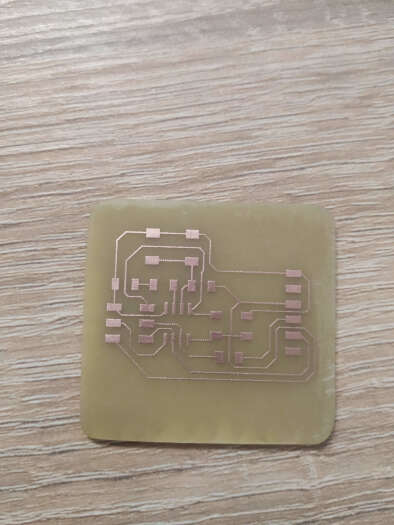
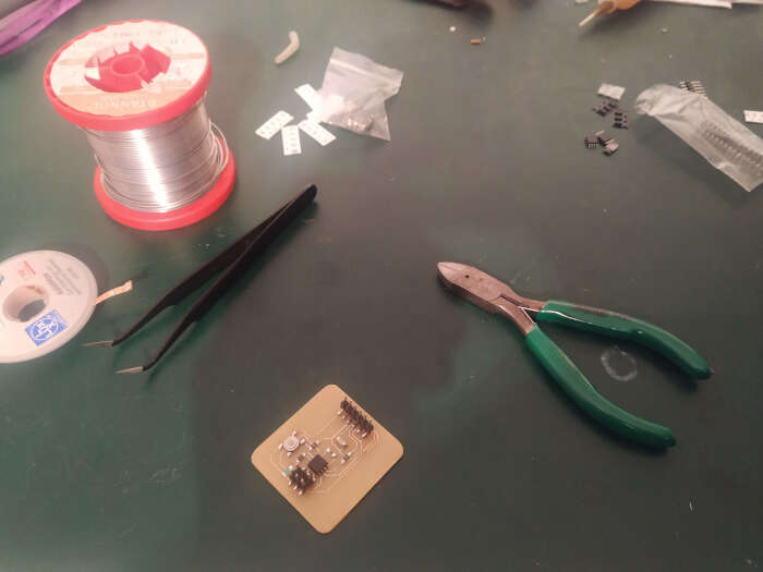
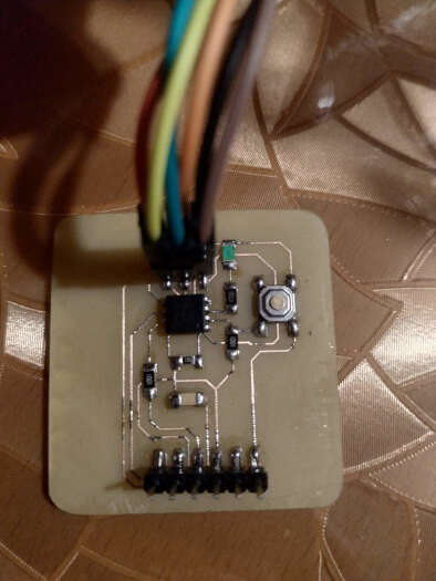
After that I started to solder the above mentioned components to the PCB. After soldering the components the results can be seen here.
Testing the PCB
Now it’s time to test it. I transfered the program onto the board using arduino software. I added ATTiny support to Arduino IDE. I followed this link. I programmed a simple sketch. When the button is pressed, the LED lights up.
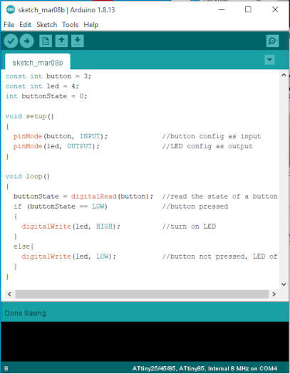
Simple sketch code in arduino
const int button = 3;
const int led = 4;
int buttonState = 0;

void setup()
{
  pinMode(button, INPUT);             //button config as input
  pinMode(led, OUTPUT);               //LED config as output
}

void loop()
{
  buttonState = digitalRead(button);  //read the state of a button
  if (buttonState == LOW)             //button pressed
  {
    digitalWrite(led, HIGH);          //turn on LED
  }
  else{
    digitalWrite(led, LOW);           //button not pressed, LED of
  }
}
You can see in the video below.
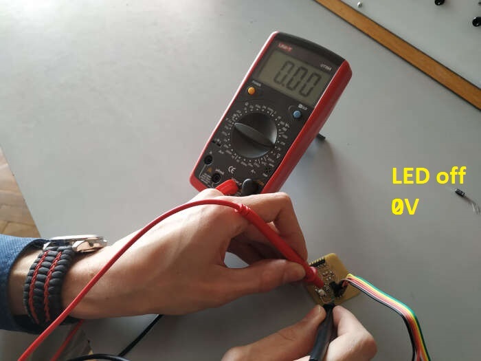
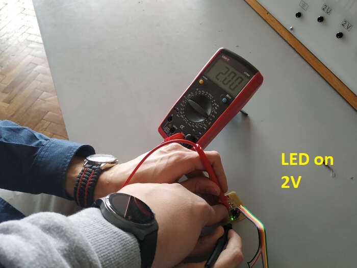
Group assignment
For the group assignment we had to use the test equipment in our lab to observe the operation of a microcontroller circuit board. I used digital multimeter to read voltages. I measured the voltage when the led is on and off. You can see in a picture below measured voltages.