6. Electronic Design
After last weeks lesson, I felt super tired. We had a lot of things going on at work and having to follow online workshops for a whole day asked too much of me. On Thursday I decided to use the time usually spent on travelling back and forth to the lab (almost 3 hours during rush time, even during the pandemic) and try to finally programme the FabTinyISP.
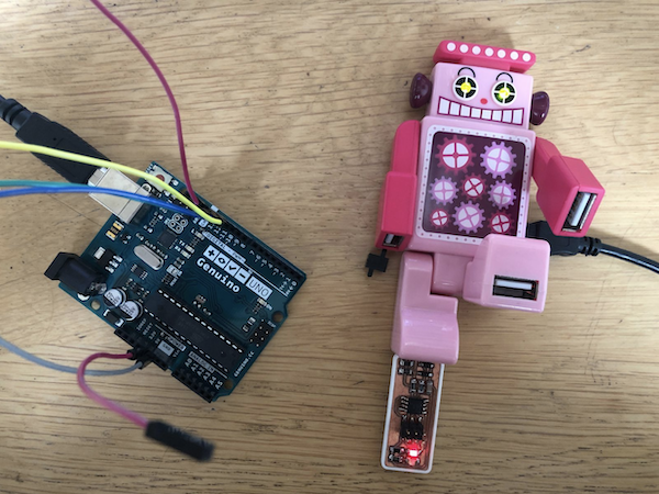
With the arduino at hand acting as an ISP, cables ready to go and my old school robot USB-hub as a mediator between the USB-c and USB I’m all set.
I followed this tutorial and it took me until Friday afternoon to get the software installed on my macbook. (XCode, Crosspack and Make).
Since it was Kurt’s birthday, we decided it would best to take time to eat cake and celebrate with gifts while researching our final project, instead of doing very hard thing. And even during al the hectic things last week, I managed to make a gift for him.
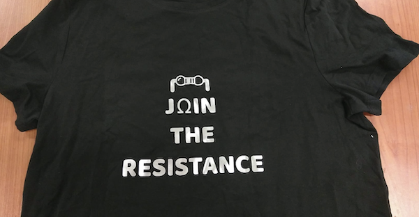
Perfect shirt to wear during the Electronic Design week!
Group assignment
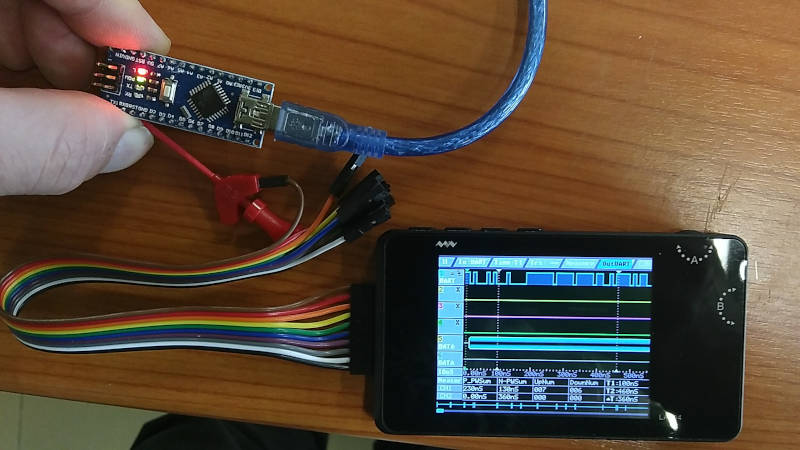
For the group assignment, we have to try out some lab test equipement. We ordered the DSO123 oscilloscope and the LA104 logic analyser to be able to use in the lab and at home.
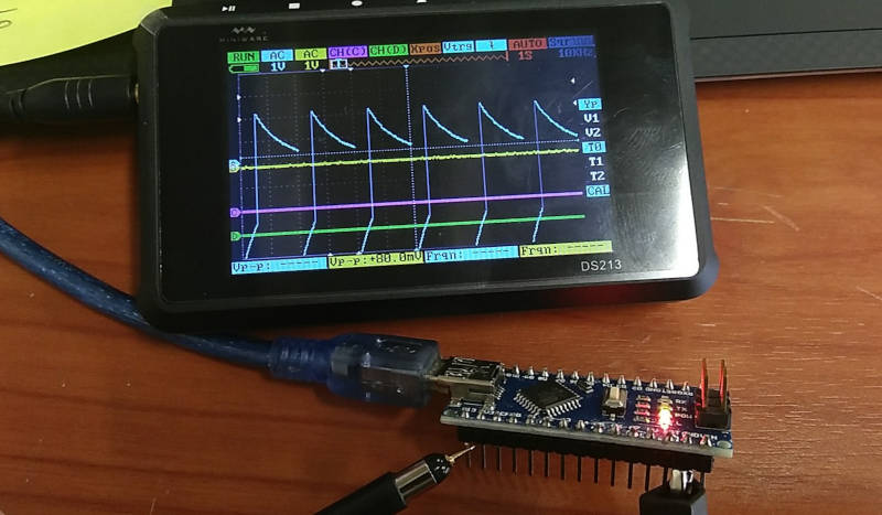
Before testing we need a subject. So we took an arduino Nano and programmed it to blink the internal LED with 500ms on time and 1500ms off time. We also have it write to the serial port. So we can test that also.
First we connect an analog channel of the oscilloscope and see the rising and falling of the voltage on the LED pin.
After that we connect the same LED pin to a digital channel and also can see the on-off sequence.
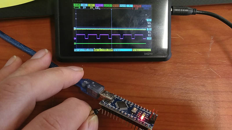
We also connected the TX pin of the arduino to the logic analyser to see data on the UART.
We still have to learn more on how to use this tool, so we have to watch some tutorials. To be able to use this at full potential.
Individual assignment
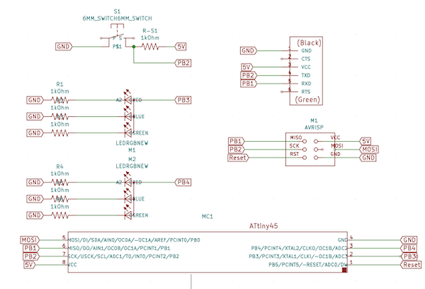
Drawing circuits is very new to me and I’m very curious to find out more. Starting using KiCad is something to get used to. But work was very hectic this week, so after Wednesday’s class I didn’t find a couple of hours to dive into the software.
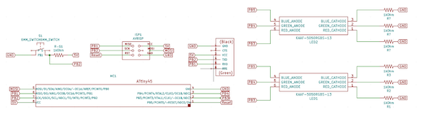
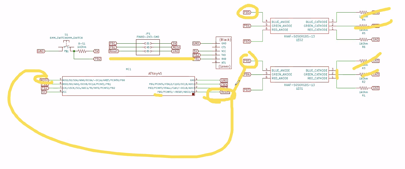
When I finally did, I noticed that if you understand the basics of electronics drawing a scheme is not very hard to do. I came up with this after a bit of drawing and re-drawing, with the help from Kurt.
This is based on the ATtiny45. A simple choice as these are the components that were already delivered. Another package is still stuck at customs. It’s a simple matter of using what we have at hand.
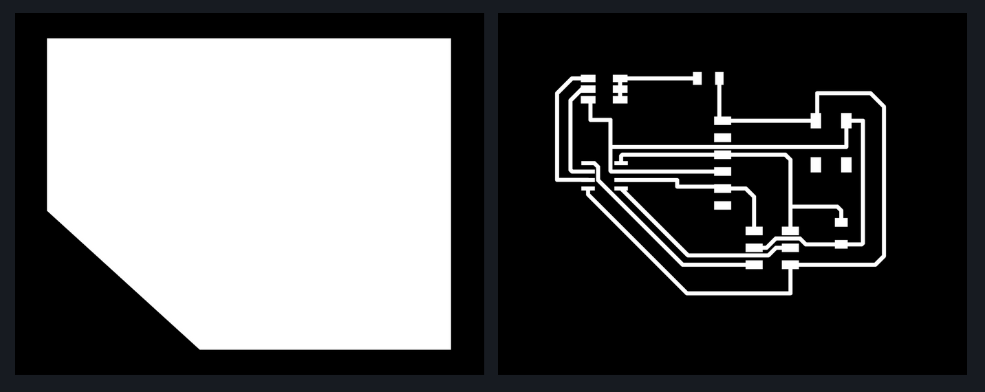
Of course, this can’t be used for milling the PCB. Therefore you need to expand the scheme into a PCB using the big green button on top at the right side.
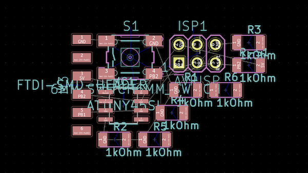
After pressing this button (make sure your footprint libraries are installed!) you get something that looks similar to this, depending on the components that you added to the scheme.
Time to start drawing traces!
But… after a good night’s sleep, I remembered that I needed to check the datasheet for the RGB leds that we have available as they might differ from the ones in the scheme. And guess what, they are different!
But hey, I’m here to learn. So I looked up the datasheet, read it and set out to download the right symbol and footprint for our parts.
I stumbled upon Component Search Engine, a website that gathers information on components and stores their symbols and footprints. Exactly what I need, phew ;-) Using the part number I quickly found the datasheet I needed. I read it, downloaded the symbol and foothprint. This allowed me to continue designing the PCB in KiCad.
Back in KiCad I updated the scheme with the right RGB led.
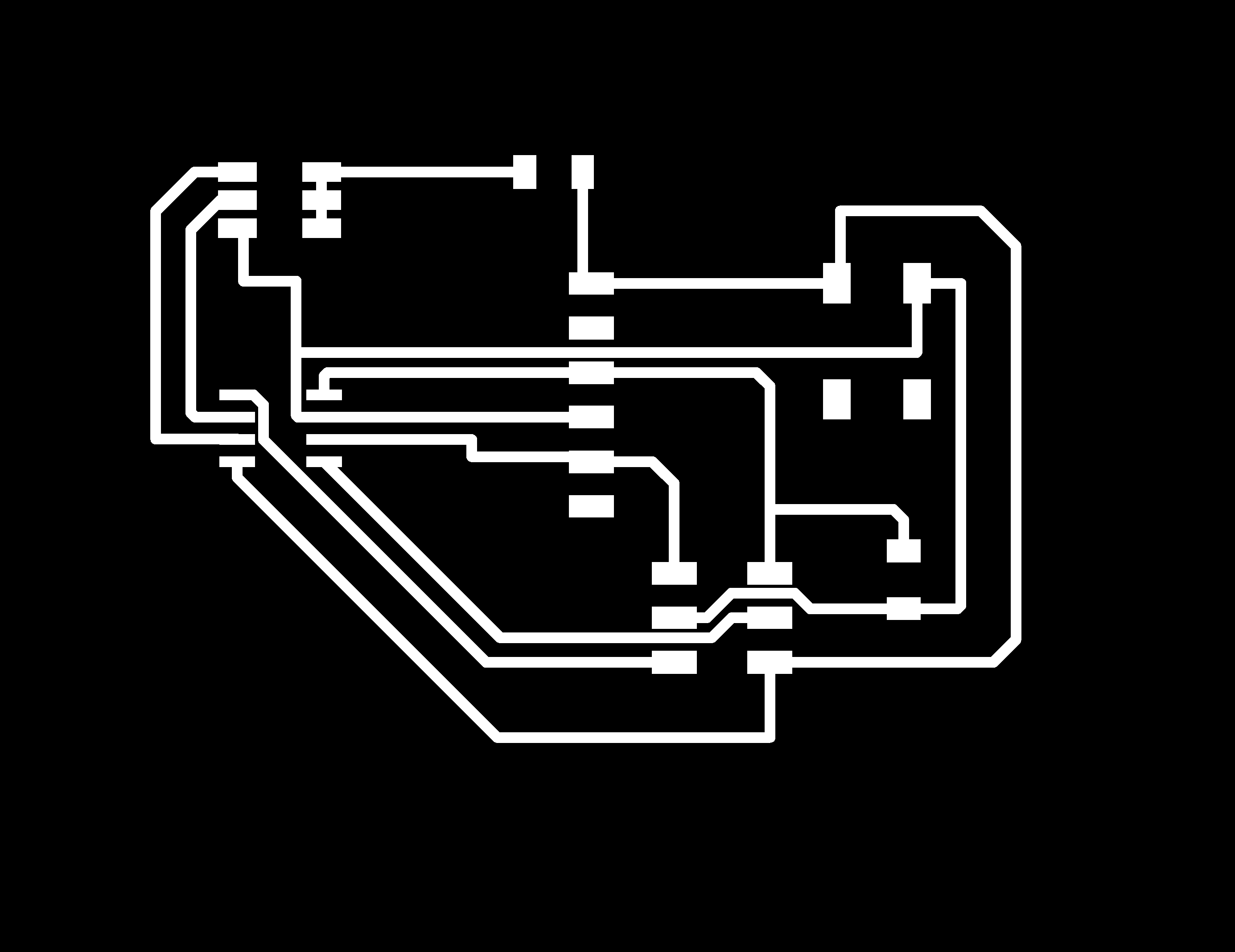
And converted into toolpaths.
Second time to start drawing traces!
But coffee first, always…
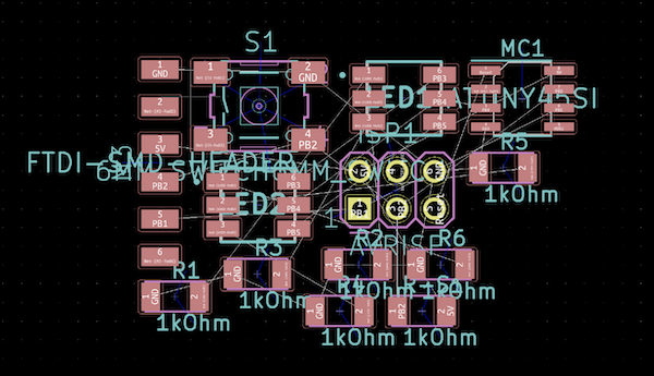
The next step in designing a PCB is to move around the different components into the basic form you which to achieve. This could be the smallest possible layout, or something a bit more artistic if you don’t want the basic PCB shapes and everything in between. You can move the parts by selecting them, you can press R to rotate them. When moving the parts around, the components are connected via white lines that are an indication of how your traces should be drawn.
I went for a basic robot style form.
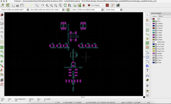
The next step is to draw the traces, you can do this by selecting the button with the green line on the right. You can just click on a component and the other components that need to be connected with the one you selected, will light up. Simple form a trace and click whenever you want the end the trace. This could be on another component or somewhere on you PCB to continue drawing later on.
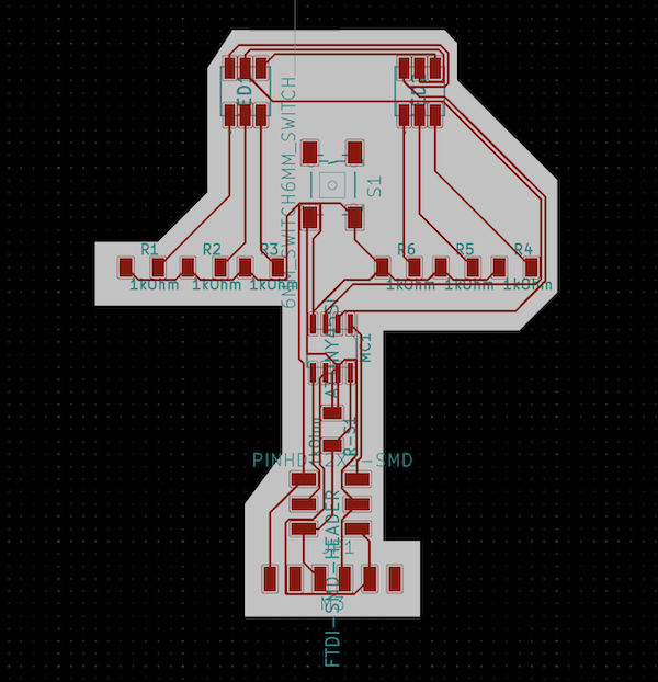
After a lot of puzzling and testing and re-drawing, I finally ended up with something that will work.
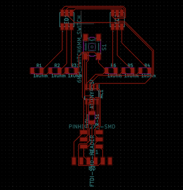
After having the traces in place, I needed to draw the shape of the PCB. I did this using the polygon tool (the blue button on the right).
When you press the little ladybug on top of the screen, you can run a test to check whether your board can be milled.
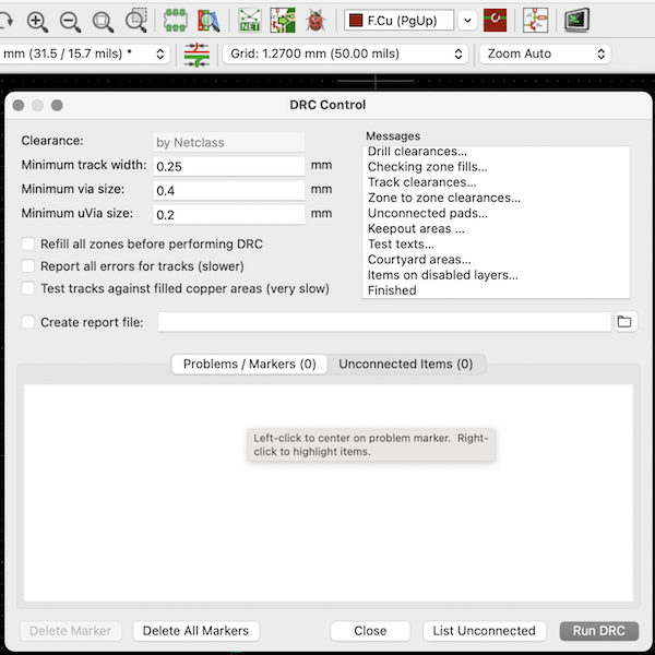
When it’s not giving you any errors, you are ready to go! Simply export the PCB to an svg and continue in vector software to create the png’s you need for the milling machine.
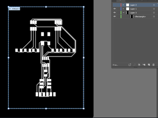
I was advised not to use Illustrator, but since I’ve been working with the software for a long time now I wanted to find out if it’s really that hard to export the PCB in a png-format in the size you need. Well, actually, your board as well as your outline need to be exactly the same size.
I imported the svg’s from KiCad into Illustrator. Copy pasted both the outline and the traces on a different layer in one single file. Creating an art board that is only slightly bigger than the outline of the PCB.
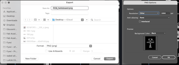
When exporting, select “Export as”. This is important! Do not select export for screen, this exports as png, but you do not have enough control over the size of the export.
You will have to repeat this step for the traces and the outline. First set your outline to invisible, this will let you export the traces first.
Just follow the steps:
- name your file
- select PNG
- select the artboard if you have multiple
- set the correct resolution
- set the background to black
- press Ok
Now repeat the steps with the traces layer hidden and the outline layer visible. Illustrator should have remembered the resolution setting, but always double check!
With these steps being done, it’s time to mill the board.
Make a Hello Board - part …
We had the review meeting with Eduardo. Thankfully I hadn’t milled the board yet as my scheme and board need some adjustments.
Taking all the feedback into account, I focused on the re-design. For now I left out 1 RGB-diode to make the design a bit less complex.
I re-made the schematic, the traces in KiCad. I exported the svg and drew the outline in Illustrator. As before, they were exported as PNG’s. One for the traces and one for the ouline.
With my new PNG’s I’m ready to mill in the lab on Thursday. Fingers crossed!
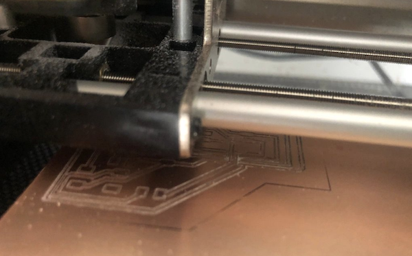
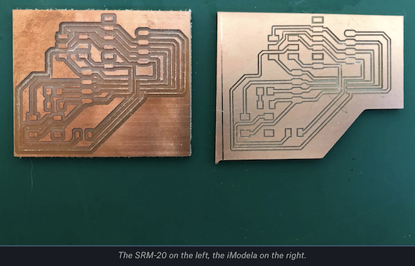
I milled a board using the SRM-20 in the lab, but I wasn’t happy with the result. So I did a rerun at home using the iModela. It took a while but the board came out really good!
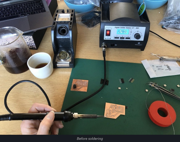
After the milling, it was time for soldering.
After soldering the board looked like this:
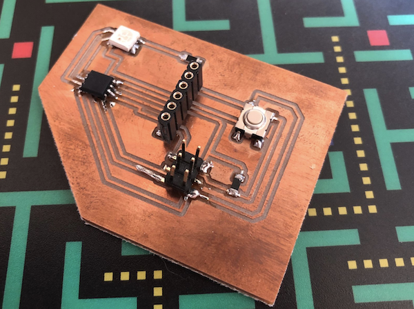
Connecting the board to the the arduino (using it as an ISP) and after burning the bootloader, I programmed the button to make the LED blink as seen below. Further programming and documentation will be uploaded during the embedded programming week.
