6. Electronics Design
Assignment
Group assignment
- use the test equipment in your lab to observe the operation of a microcontroller circuit board
Group Project here
Individual Assignment
- Redraw an echo hello-world board
- Add (at least) a button and LED (with current-limiting resistor) check the design rules, make it, and test it.
Extra Credit : simulate its operation
Electronics design
Process
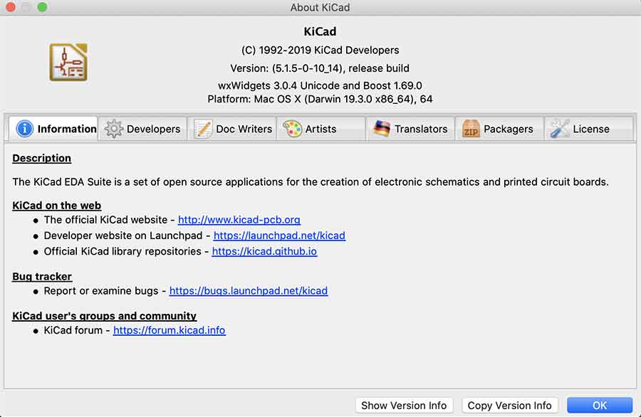
- This week's electronics design started with KiCad()
→Download Kicad link

- ↑"KiCad" version downloaded
- Click "Create New Project" and Make the project folder → Open the "Schematic Layout Editor" → Click the "place symbol"(red block!)
- (But My MacBook didn't have "symbols".(Our MacBooks were all like that)
So I downloaded "symbol libraries" here.)
→ Download "sparkfun"/ "fab"/ "digikey"/ "ORL"(-made by "seeed" company by Jessy )
- Preferences > Manage Symbol Libraries > "Add all you download."
- Now draw.(thank you Jessy!!)
- I referred to this link.
- First, add the symbols I need, and then connect them with a wire.
- There was not enough space, so I used the "Place global label" to connect.
- And click the "Annoate Schematic" and annoate → Edit value of RES
Check and fix the "Electrical Rules Checker"(I have 2problems)
I made a miso rx tag and didn't connect it to the rx pin. So there are two problems that have occurred. I removed the tag and just connected it with a wire. The problem has been resolved.
- Add this week's assignment: LEDs and switches
- This time, add the FootPrint libraries and do "Assign Footpronts" → Click the "Netlist" > "Generate Netlist" > "Save" → Go "Run Pcbnew to layout circuit board"
- File > Board Setup... > Modify value of "Net Classes"(if use to 0.4mm)
- Clearance : 0.42
(There was an error that said that could not be cut in the "BANTAM", so I left a margin of 0.02mm.)
- Track Width : 0.4
- Via Size : 1.2
- Via Drill : 0.8
- uVia Size : 1.2
- uVia Drill : 0.8
- aPair Width : 0.4
- aPair Gap : 0.4
- Clearance : 0.42
- Do design and make edge cut lin.
- Click the "Perform design rules check". Very Important!
- ↑This problem is okay because it did not pass through the clearances of 0.42mm did not work, so it changed to 0.4mm
- Must be checked here both "Problems/Makers" and "Unconnected Items"
(A disaster has come to me because I didn't check "Unconnected Items".... Scroll down if you want to know what's going on)
- Finally, Printed my design board and check the size with component needed
- It's time to plot! Check only needed layer
- I used the bantam tool to pull out my board and remove unnecessary copper for short circuit.
- CLEAR~! Do Soldering!!
- Done!
(I was happy up to here. Like the fourth week. But just a little scorched)
Now I'm programming. In order to programming, I need atinycore is required.
- Testing the Board in Arduino IDE! Well done! (But I have behind story... Now I'll let you know.)
My Behind Story
- The first problem when I connected my board to a computer, Looked a red light on the isp, not a green light. But when I pressed the switch, It was changed to green light.
- I thought it was okay, so I pressed the button to program it.
- Then Craig finally found out.!!!
This Fact!!!
- In Fact, I didn't check for "unconnected items" in the DRC.
It was very dangerous, and I was told it could explode. So I connected it with a wire and made it look like a mushroom cloud.
There was a problem afterwards, I thought it was maybe FTDI communication error.
- In the end, my board had to look like this....
File
- KiCad_Demo brd File here
- KiCad_Demo-F_Cu.gbr File here
- KiCad_Demo-Edge_Cuts.gbr File here
- KiCad_Demo-F_Cu.gbr_2 File here
- KiCad_Demo-Edge_Cuts.gbr_2 File here
- KiCad_Demo.sch File here