final project: split typing/musical keyboard - build log
In week 02 I experimented with different CAD tools to draw the keyswitches and possible designs for keyboard shell for the original ergonomic keyboard computer idea.
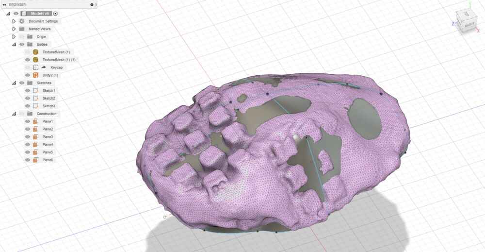
I quickly noticed that designing complex curved shapes from scratch was not very feasible, so in week 05 I tried a very different approach and modelled two different keyboard shapes using salt dough and digitized them using photogrammetry.
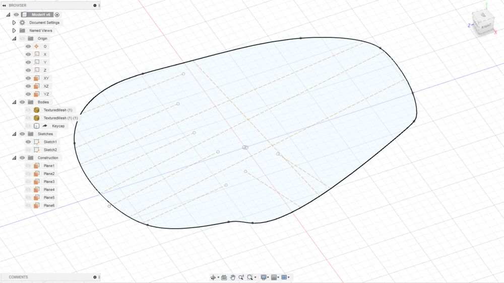
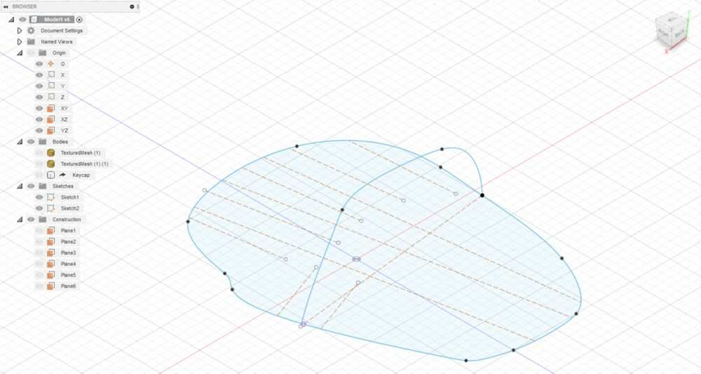
I then imported one of the resulting meshes into Fusion 360, cleaned it up
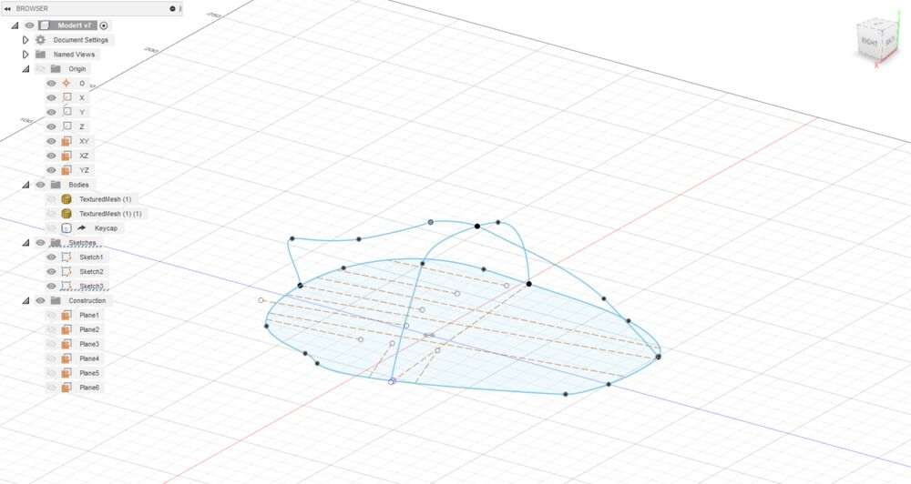
and traced the shape. I drew one “ground plane” sketch and then created
multiple section sketches. Using the Surface > Patch feature I then could
roughly recreate the original shape:
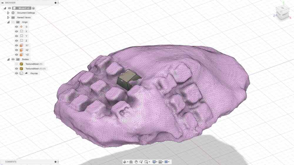
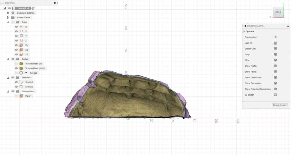
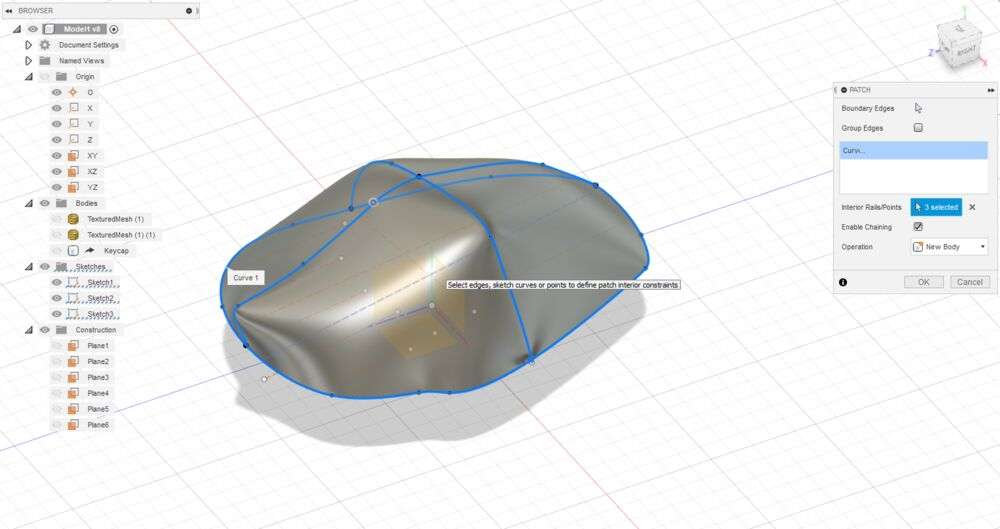
(The result has very noticeable spikes here because it uses a single section sketch, with more sections it became considerably smoother).
redesign
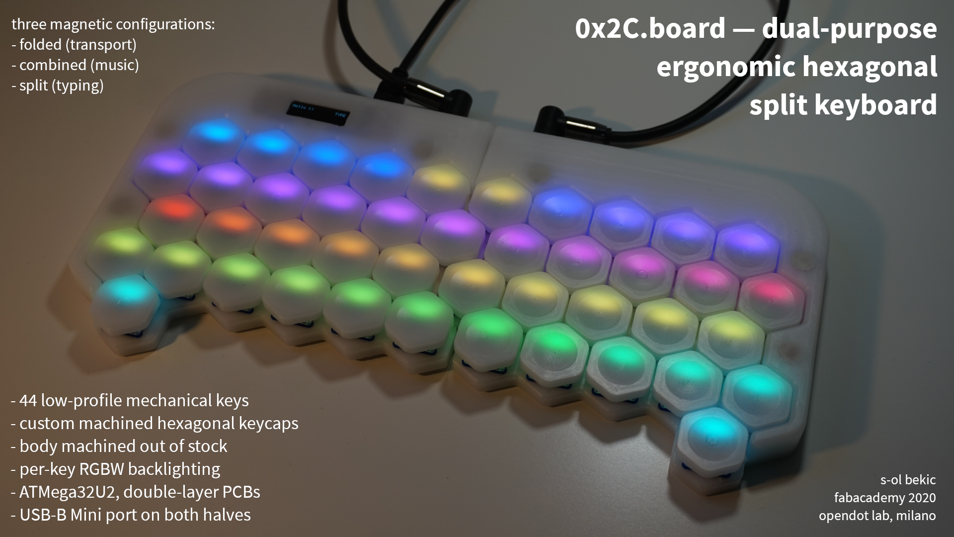
For week 15 (molding and casting) I started working on hexagonal keys. Originally I wasn’t going to use them, but after being very surprised by the results, and increasingly frustrated with the old design and idea, I changed focus and decided to merge another project from my ‘idea pile’ into this: Ever since seeing a 3d printed modification to an off-the-shelf MIDI keyboard that retrofitted hexagonal keys to create a ‘Janko’ layout, I wanted to build something similar. I also thought it would be nice to use translucent keys in a single color and highlight the active scale using per-key RGB lighting, rather than using fixed colors to show the C major scale.
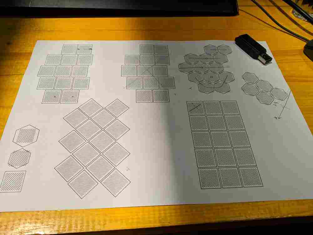
I printed hexagonal grids at different sizes and spacings and started planning a keyboard layout that would be useful both for typing and musical use.

I realized that for typing, ideally the hexagonal grid would be arranged in staggered vertical columns that align with each finger, whereas the Janko layout requires the “other” configuration, with keys arranged in horizontal rows. The difference between the two layouts is essentially just a 30° rotation, so I designed the keyboard as two halves that can be rotated into the vertically-staggered typing configuration, and assembled together to form a larger horizontally-staggered surface for musical use.
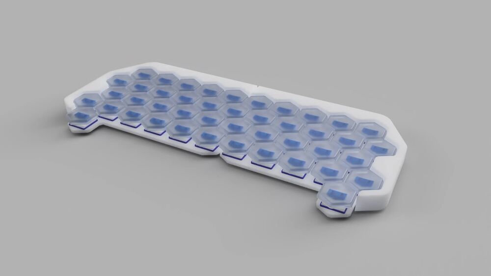
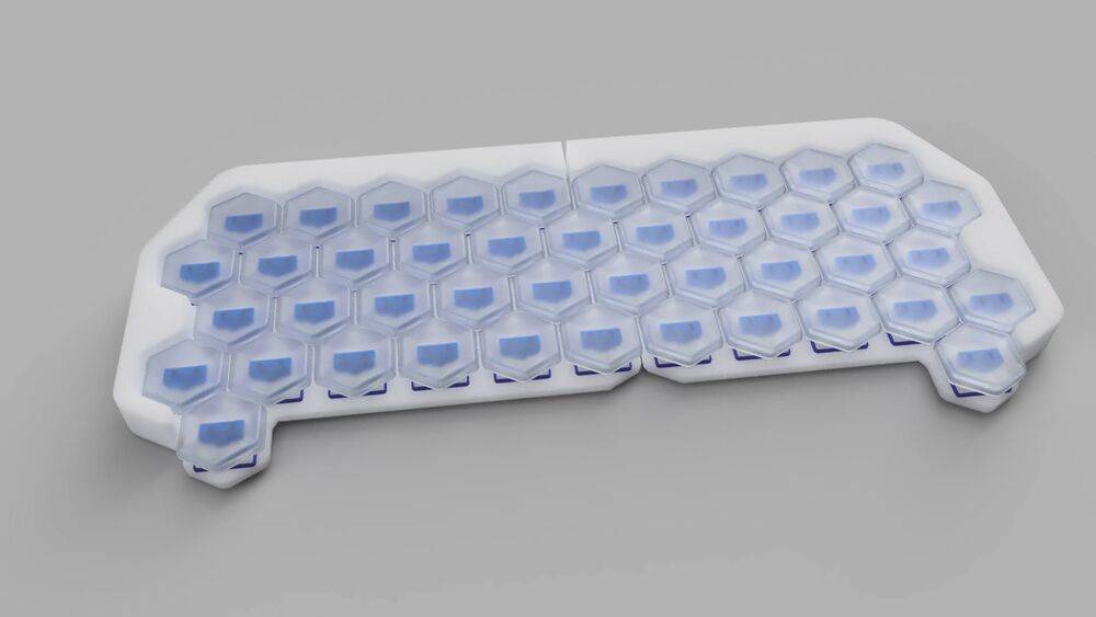
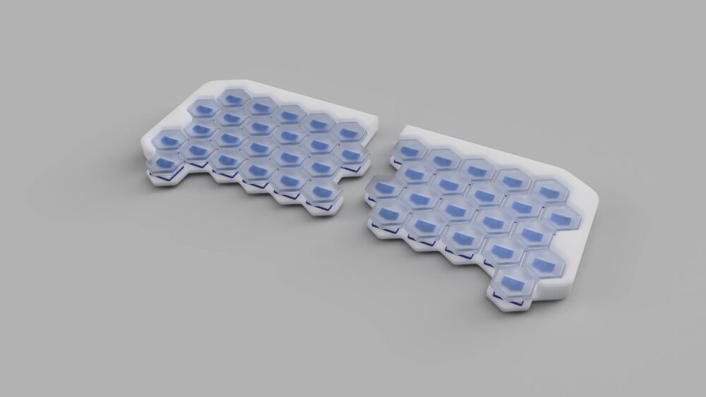
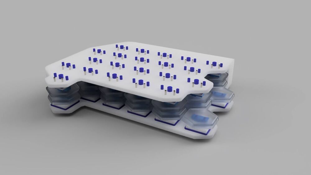
Adding a guard around the top and sides of the keyboard yielded desparately needed space on the PCB (for the MCU and connectors) and a visual surface (for indicator LEDs or possibly a display), and allows the two halves to be folded on top of each other for transport:
LED + switch mounting
I used RGBW ‘Neopixels’ in the 5050 package for the backlighting. The
manufacturer part name seems to be SK6812 (see the datasheet).
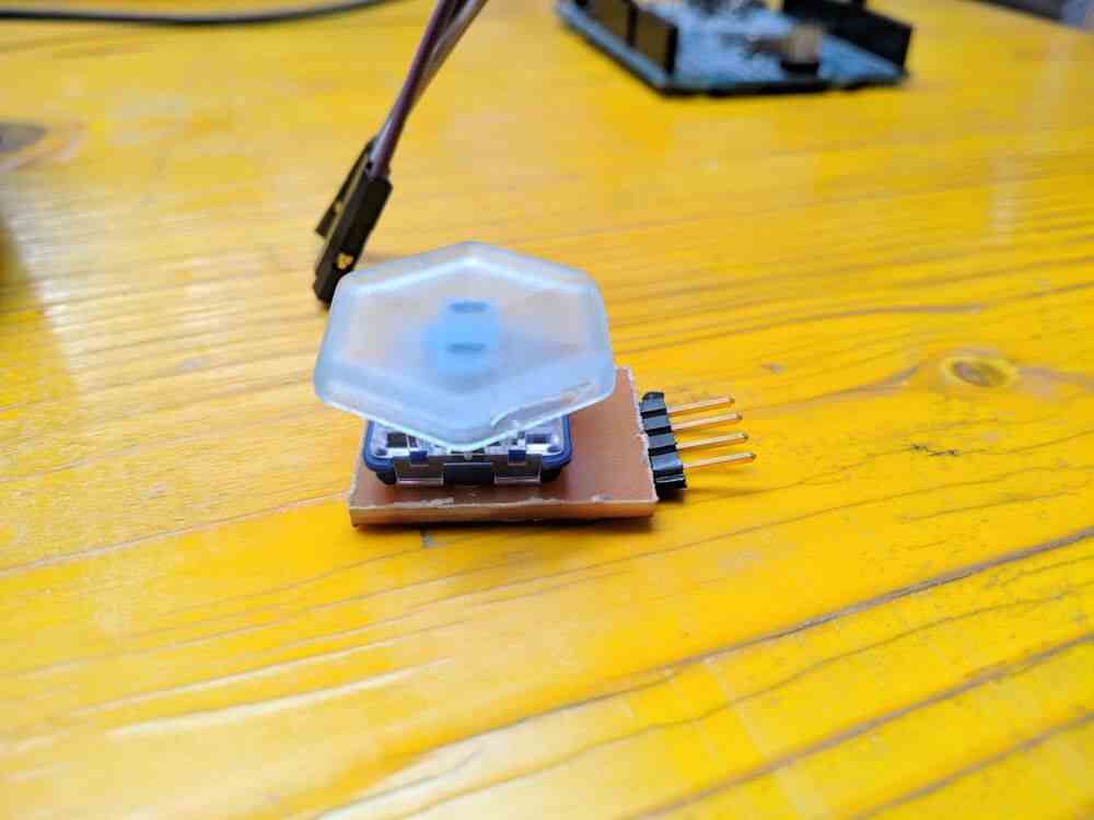
The keyswitches have a little hole in the bottom plastic for an LED to peek through to the transparent top, but the hole is only ~5x3mm large and even smaller LEDs would be very hard to mount precisely inside it. Instead I tried a different solution: milling out a pocket in the PCB for the LED to sit in, and ‘reverse mounting’ it inside the PCB.
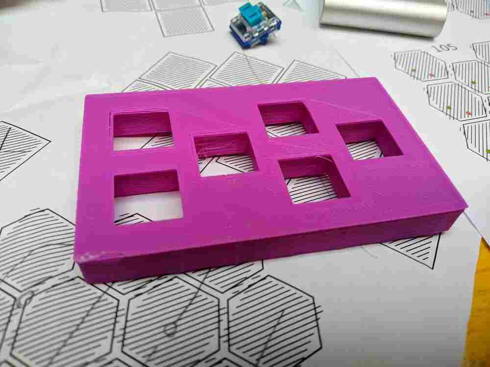
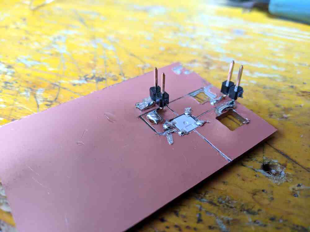
I designed a mechanical test in Fusion 360 and milled it on the Roland MDX, then scored the PCB to create four large pads to solder the LED and some header pins to:
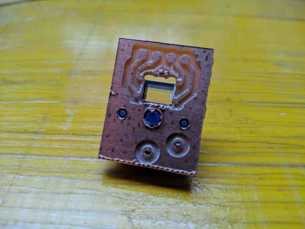
This worked reasonably well, so next I created a compatible KiCAD footprint and routed a little test board to figure out the workflow between KiCAD and Fusion360. I realized that from KiCAD I can plot the copper layer as a DXF, and then use an engrave pass to do the CAM in Fusion. The first test came out with a good mechanical fit on the keyswitch:
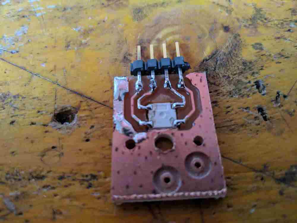
and also soldered well:
electronics design + production
MCU test board
The electronics were designed in KiCad and are mainly a mix-and-match of the following excellent resources on designing keyboards in KiCad:
- ruiqimao’s “keyboard-pcb-guide”
- masterzen’s “Designing a Keyboard from Scratch”
- “Keyboard Designer Guide” on the ai03 wiki
I started with the MCU and made a prototype PCB that has just three keys and LEDs using the footprint I designed earlier. This let me verify my MCU and USB design before investing time in routing the full PCB and potentially wasting resources on manufacturing full-size PCBs that weren’t going to work.
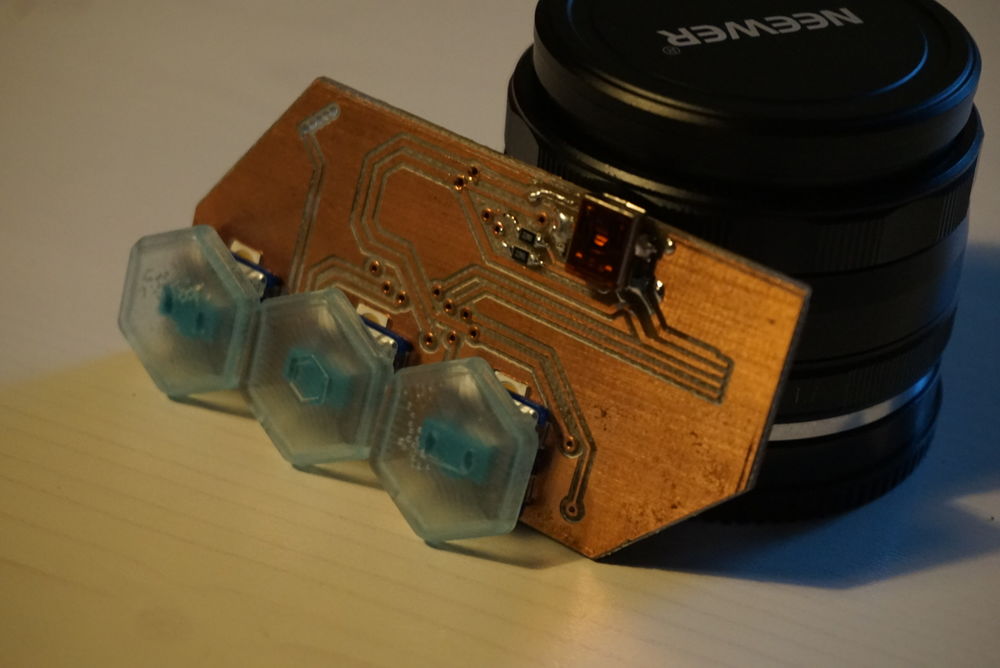
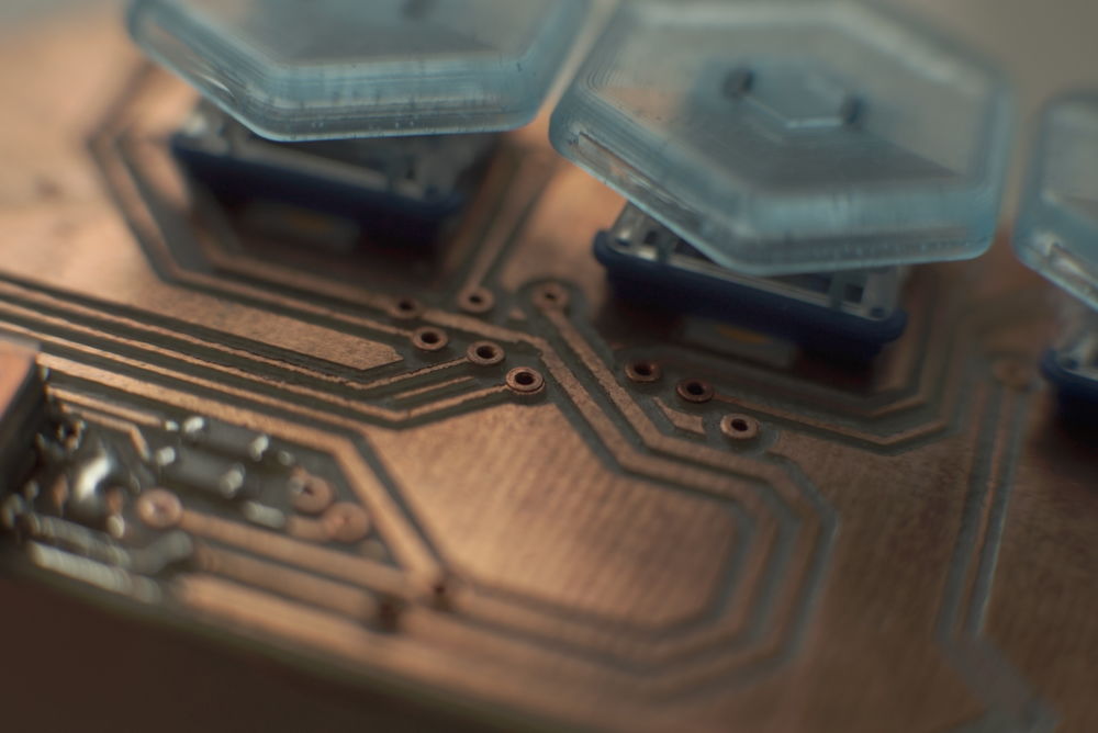
I knew from the beginning that the full-size board needed to be a two-layer board, since the switch matrix requires lots of more or less orthogonal traces, which is further complicated by the RGB LEDs that also have to be routed in the same space. To get a feeling for double-layer boards, I didn’t try to design this prototype as a single layer from the start although this may have been possible. I figured out as a consequence that the copper rivet vias I was using make good contact on their own in the beginning, but then start to slowly fail intermittently after some weeks of use. By simply soldering the rivet to the via pad this can be solved preemptively. I put in all vias such that the pre-formed side is on the top of the PCB, where the PCB later has to lay flush against the top plate of the case, in order for that contact to be more consistent. The side where the rivets have to be hammered into shape are then on the more accessible bottom side of the PCB:
full design
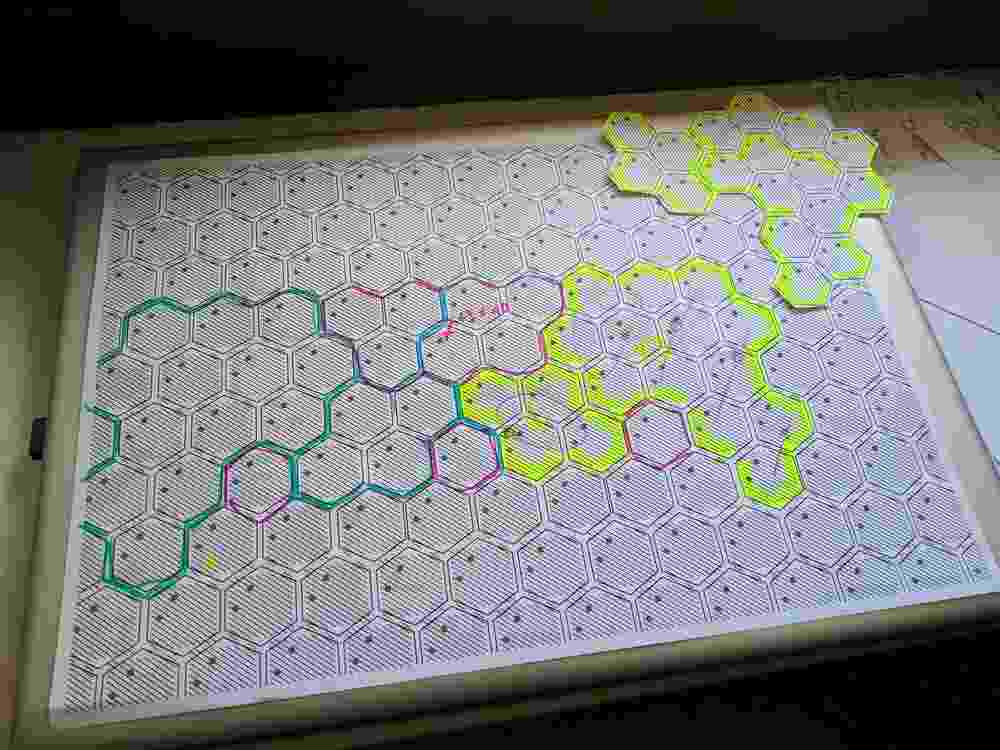
Once I was confident in the general design, I worked away on the full version, which consists of two copies of the MCU curcuit and two matrices that have slightly different shapes in order to optimize the matrix layouts (the right hand uses a 6x4 matrix with three unused crossings, while the left hand uses a 5x5 matrix with one unused crossing). I also designated one GPIO pin to be tied high on one side and low on the other, so that I can flash the same firmware to both halves and the code can detect the correct configuration at runtime.
When routing the PCBs, I placed the two halves in the unified configuration, so that I could route it essentially as one big keyboard with a very thin cut down the middle. This let me place all the keys on one consistent grid and also let me check the fit on the pogo pin connector that allows communication between the boards when attached together.
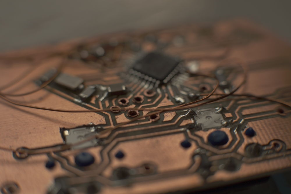
Almost all components are placed on the underside of the PCB, so that the board can be pushed flat against the case on the top. Only the board connectors (USB, TRS and pogo pins) and a minimal amount of passives are placed on the top side, inside of the back margin of the board where a matching cutout was added to accomodate these.
I designed the case of the keyboard and the PCBs at the same time and often pushed the board outline back and forth between KiCad and Fusion 360 in this process. The interactive BOM is a really useful reference while soldering, and also gives a good idea of the PCB overall.
PCB production woes
Manufacturing the full-size PCBs turned out to be a much bigger challenge than I expected. While each half fits on the 152x152mm blanks I was using, it uses almost all of that are and is much bigger than most designs that are routinely made using the milling process we use at OpenDot. When I started milling the PCBs, it quickly became clear that they were not even enough to engrave at a single fixed Z depth without cutting either to deep in some, or too shallowly in other places.
A seemingly straight-forward workaround is to divide the engraving job up into multiple smaller regions and zero the Z axis separately for each job. This also opens up the opportunity to adjust the workholding between regions.
Large PCB designs will invariably have at least two tracks (power) that span the whole board and have to be cut up. Generally the same will have to be done with many other tracks, since variations in board height can be excessive enough to make milling in a single pass impossible even within ~40mm distance. The problem with slicing the toolpaths up is that most CAM software doesn’t have any tools to do so, so it might be tempting to instead slice up the input files, for example a DXF. However simply cutting the toolpath will leave the toolpaths “open”, so the CAM software will either not be able to mill with an offset or close the individual parts off, resulting in cut traces in the result:
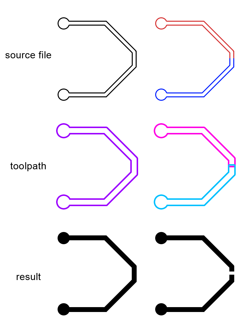
The only way to get around this is to manually offset the trace outlines and then chop them into groups afterwards. In practice it turns out that Rhinos offsetting algorithm isn’t good enough, so the best workflow I found was to export to DXF from KiCAD, clean up the file in Rhino, then bring it into VCarve, create multiple offsets, then export back to Rhino, cut the offsets into different zones, import again into VCarve and finally create all the CAM paths. Almost all of these steps involve a lot of repetitive manual work and every change in the PCB means starting back from zero.
I tried using this technique and spent one and a half days getting the CAM ready. When I went on to actually mill it, I managed to get the first (simpler) side of the PCB to a just about useful quality, although in two spots a track was stripped entirely and would have needed manual repair.
When I moved to the back side it quickly became obvious that the seven zones I cut the job into where just way too large. I aborted the attempt at that point and instead tried preparing files for an attempt using the laser-exposed PCB etching process. Just short of the finishing line it turned out that Rhino 5 was simply not able to hatch a a shape of the size and complexity of my ground plane without crashing, which was quite the disappointment (as it usually is, when production software fails to scale at a seemingly arbitrary point…). I channeled the accumulated frustration into something positive and developed an autoleveling tool suite for OpenSBP CNC machines that finally allowed me to produce PCBs of this size consistently and with much less preparatory effort (see the linked page for more information).
case + mechanical design
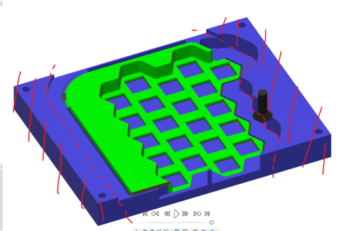
After a lot of experimentation using 3d printing, which was very useful for testing the key spacing and the dimensions of the snap-fit that retains the keyswitches, I decided to machine the case out of POM since I really liked the machined finish we got out of the POM parts for our machine-building project and the white color of our stock would work well with the RGB lighting as well.
I designed the case in Fusion 360, using DXF files exported from KiCAD to make sure the electrical components would all line up with their corresponding cutouts. The design went through a variety of changes until I settled on the final shape, with a thick border on the back and thinner ones around the sides, while keeping the characteristical jagged hexagonal outlines on the front of the keyboard.
I also incorporated four holes for magnets in matching locations on each half to allow for the magnetic snapping in the typing and transport configurations. Three of the magnets are sunk into blind bores that go from the back of the keyboard until about 0.5mm below the surface of the keyboard and hold the halves together firmly when folded over. Near the pogo-pins that connect the two halves in the typing configuration a magnet is inserted into a rectangular slot and held in place by the PCB, which is mounted over the magnet.
The PCBs are held in place firmly by the two soldered leads of the 21/23 keys, but I also added three tapped M3 holes to screw the board into the case from below.
case machining
I did the CAM work in Fusion as well. There are six different setups and 17 operations involved in making one half of the case.
setup 01: planing the work surface
Since the case needs to be very flat to be able to rest properly on the table, and there are some very tight tolerances involved with some of the features along the Z axis (such as the blind holes for the magnets), it is crucial to have a good Z reference and a flat work surface at the start of the process.
A very easy way to achieve this is to start with a fresh sacrificial piece of wood to use as a fixture, and plane it with the same tool that will be used for the following operation.
setup 02 + 03: roughing + detail (front)
After the work surface is planed, the POM stock is attached with a couple of screws. The front can then be worked using the freshly surfaced sacrificial layer as a reference.
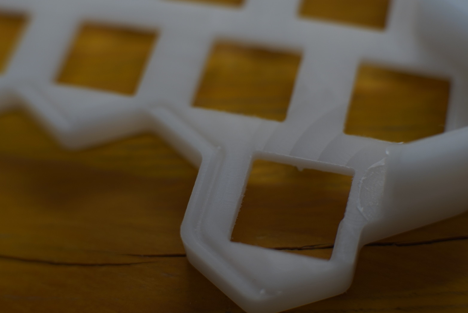
I’m using a 6mm flat mill for the roughing and to bring the stock to a known and parallel Z thickness, before cutting out the key-holes and finishing the inside contour with a 3.175mm flat endmill. Then a 1.5mm endmill is used to clean up the key cutouts and lower their corner radii, so that they can snap in without the need for dogbones.
Finally, some of the edges are chamfered using a chamfer mill to add some visual detail and remove burrs from machining.
setup 04: back fixture
Now the part is removed, but before the back can be machined, a fixture that holds on to the front features has to be cut. I’m using the 6mm and 3.175mm mills again to create a pocket matching the outline of the raised parts of the case.
interlude: cleaning up the part
Before the stock fits into the new fixture, some of the excess that hasn’t been trimmed down by the front passes has to be trimmed off manually on the bandsaw.
setup 05 + 06: roughing + detail (back)
Now the stock can be placed back down into the fixture and screwed down again using the new mounting holes created in setup 03. The 3.175mm and 1.5mm endmills and the chamfering tool are used to cut various pockets and bores. Then the keyboard has to be wedged down by an extra piece of wood screwed through the key cutouts in the center while the outline is cut, leaving just the finished case.
gotcha
Hmm, this doesn’t look quite right… the chamfer is in the wrong place, and the key cutout isn’t centered where it should be!
Something is wrong. Did you spot it? It took me another failed attempt and over a week of sherlocking to figure out what was going on:
The fixture looks like it completely locks horizontal movement of the stock, but it actually leaves one degree of freedom! Since there is a lot of friction anyway, I never noticed this while putting the stock back in, resulting in an offset between the front and back operations and useless parts.
Once I knew what the problem was, it was just a matter of carefully hammering the stock into position before screwing it down when placing it in the fixture. E voilà:
firmware
bare-metal firmware
While testing the board I wrote a small firmware from scratch to verify that all the components were working as expected and familiarize myself with the AVR workflow.
This firmware is checked into the project repository in the firmware
directory. It uses the avr-gcc toolchain and a simple Makefile to
build and flash the project.
The code for the OLED display and RGBW LEDs was borrowed from other open-source
projects like QMK (see below) and is fairly simply in its usage. For the LEDs,
it is enough to simply call the function ws2812_setleds with the binary
containing the RGBW values (one byte per component) and the number of LEDs, and
for the oled screen there are just a couple of handy library functions to turn
the module on, print to it and clear the screen. The oled code did require some
changes to get it to work on the ATMega32U2, which does not have a native I2C
peripheral. I found a software I2C implementation and hooked the two into each
other which worked fine right away.
To read the keyboard matrix, first all the row-pins are configured as inputs
(and the builtin pullups are activated, DDR??=0, PORT??=1). The column-pins
are tristated (DDR??=0, PORT??=0), so that they do not interfere at first.
Now one column at a time is set to be an output (DDR??=1) and the row-pins
are sampled. Wherever a key is pressed in the current column, the switch will
make a connection between the row-pin and the column that is now at 0V, turning
the output into a zero, which is registered as a keypress.
After sampling all row-pins, the column has to be tristated again before the
next column is activated.
To make sampling the rows easier, I tried to keep the row-pins on one or two
GPIO ports and in order. This way the whole PIN? register(s) can be sampled
at the same time and some simple bit-math yields a single byte bitfield per
column:
    // different pin configurations for right and left hand
uint8_t is_left;

uint8_t state[COLS][ROWS];

void read_rows(uint8_t col) {
  if (is_left) {
    uint8_t row = PINB;

    for (uint8_t i = 0; i < ROWS; i++)
      state[col][i] = (state[col][0] << 1) | ((row >> i) & 1);
  } else {
    uint8_t row = ((PINC >> 7) & 0b1) | ((PIND >> 3 & 0b1111));

    for (uint8_t i = 0; i < ROWS; i++)
      state[col][i] = (state[col][0] << 1) | ((row >> i) & 1);
  }
}

void scan_keys() {
  if (is_left) {
    DDRB &= ~0b1111; // set rows as input
    PORTB |= 0b1111; // set pull-up

    DDRD |= 0b111100; // set Cols/D as output
    DDRC |= 0b100;    // set Cols/C as output
    DDRB |= 0b10000;  // set Cols/B as output
    PORTD |= 0b111100; // set Cols/D hi
    PORTC |= 0b100;    // set Cols/C hi
    PORTB |= 0b10000;  // set Cols/B hi

    // check d5
    PORTD &= ~(1 << 5);
    read_rows(0);
    PORTD |= 1 << 5;

    // check d4
    PORTD &= ~(1 << 4);
    read_rows(1);
    PORTD |= 1 << 4;

    // check d3
    PORTD &= ~(1 << 3);
    read_rows(2);
    PORTD |= 1 << 3;

    // check d2
    PORTD &= ~(1 << 2);
    read_rows(3);
    PORTD |= 1 << 2;

    // check c2
    PORTC &= ~(1 << 2);
    read_rows(4);
    PORTC |= 1 << 2;

    // check b4
    PORTB &= ~(1 << 4);
    read_rows(5);
    PORTB |= 1 << 4;
  } else {
    DDRC &= ~0b10000000; // set rows/C as input
    DDRD &= ~0b01111000; // set rows/D as input
    PORTC |= 0b10000000; // set rows/C pull-up
    PORTD |= 0b01111000; // set rows/D pull-up

    DDRB |= 0b11110001;  // set Cols as output
    PORTB |= 0b11110001;  // set Cols hi

    // check 1
    PORTB &= ~(1 << 0);
    read_rows(0);
    PORTB |= 1 << 0;

    // check 2
    PORTB &= ~(1 << 4);
    read_rows(1);
    PORTB |= 1 << 4;

    // check 3
    PORTB &= ~(1 << 5);
    read_rows(2);
    PORTB |= 1 << 5;

    // check 4
    PORTB &= ~(1 << 6);
    read_rows(2);
    PORTB |= 1 << 6;

    // check 5
    PORTB &= ~(1 << 7);
    read_rows(2);
    PORTB |= 1 << 7;
  }
}
QMK
QMK is an open-source project that provides highly customizable firmware for keyboards. It supports a wide range of AVR and STM32 MCUs and has tons of features, including RGB backlighting and USB MIDI support, which makes it ideal for this project.
The QMK repository contains code and configuration for a lot of third-party
hardware that is compatible, so the configuration for this project is currently
tracked as a keyboard called hexboard in a fork. Hopefully it can be
upstreamed in the future. In case that the fork repository goes offline in the
future, a patch file is attached at the bottom.
Using the QMK tool, the firmware can be built and flashed using the following command:
$ qmk flash -kb hexboard -km default
flashing
The ATMega32U2 ships from the factory with a DFU bootloader that allows it to be programmed via the USB peripheral, which is very handy and means there is no need for an extra debug header on the board.
When the MCU is connected to a PC for the first time, it directly enters the
bootloader because the flash is empty. It can then be programmed using
avrdude (-c flip1) or dfu-programmer.
Once a firmware is flashed to the MCU, it boots into the firmware by default. To enter the bootloader again, the MCU has to be reset while the power is still connected. On my PCBs I left two pads near the MCU that are labelled RST and reset the MCU when bridged with tweezers or another conductive object.
While development, it can be annoying to reset the MCU manually for every code change. Often it is much more convenient to perform the reset from within the software, once the basic functions are implemented. In the bare-metal firmware, I implemented that using the following snippet from the QMK source:
#include <avr/wdt.h>
#include <avr/io.h>
#include <avr/interrupt.h>
#include <util/delay.h>

#define ATTR_INIT_SECTION(SectionIndex) __attribute__ ((used, naked, section (".init" #SectionIndex )))
#define ATTR_NO_INIT                    __attribute__ ((section (".noinit")))

#define MAGIC_BOOT_KEY            0xDC42ACCA
#if __AVR_ATmega16U2__
#   define BOOTLOADER_START_ADDRESS  0x0800 // (FLASH_SIZE_BYTES - BOOTLOADER_SEC_SIZE_BYTES)
#elif __AVR_ATmega32U2__
#   define BOOTLOADER_START_ADDRESS  0x3800 // (FLASH_SIZE_BYTES - BOOTLOADER_SEC_SIZE_BYTES)
#else
#   error "Unknown device name " __AVR_DEVICE_NAME__
#endif

uint32_t boot_flag ATTR_NO_INIT;
void reset_check_bootflag() ATTR_INIT_SECTION(3);

void reset_check_bootflag() {
    // If the reset source was the bootloader and the key is correct, clear it and jump to the bootloader
    if ((MCUSR & (1 << WDRF)) && (boot_flag == MAGIC_BOOT_KEY)) {
        boot_flag = 0;
        ((void (*)(void))BOOTLOADER_START_ADDRESS)();
    }
}

void reset_dfumode() {
    // Disable all interrupts
    cli();

    // Set the bootloader key to the magic value and force a reset
    boot_flag = MAGIC_BOOT_KEY;
    wdt_enable(WDTO_250MS);
    for (;;);
}
This allows resetting into the DFU bootloader by simply calling
reset_dfumode(), e.g. in response to a button press or debug key combination.
files
- bare-metal firmware
hexboard.patch: hexboard support for QMK