7. Electronics design
Group assignment
To use test equipment to observe the operation of a microcontroller circuit board.
Individual assignment
Redraw an echo hello-world board. Add a button and/or LED with resistor. Check design rules. make it, test it.
Planning
Laying out a circuit board is a difficult process. Routing tracing between components that don’t cross each other while maintaining basic design rules takes planning. Before starting this project, I defined rulesand laid out a plan. I based the design to match the characteristics and limits of the Shopbot desktop I learned during the electronics production week.
I chose the ATtiny1614 echo board.
Rules
-
Must include two buttons and two LEDs with current limiting resistors. 1
-
Be able to fit two circuits on one 2” x 3” (50mm x 16mmm) copper board. This is to minimize waste if multiple need to be cut.
-
Design circuit to be cut on the Shopbot desktop.
-
Use 1/64” end-mill
-
Traces between 0.024” to 0.030” (24-30 mils)
-
Clearance between traces 0.020” to 0.030” (20-30 mils)
-
-
Avoid 45° traces if possible
-
Buttons opposite of pin-headers
-
Include 10KΩ resistors for push-buttons
-
Do not use a 0Ω resistors as jumpers
-
Make it look professional
The process
I chose to use KiCad for this due to it being both open-source and free. It also has a large community and is supported by many parts suppliers.
Dr. Gershenfeld provides a tutorial video showing the basic work flow of KiCad:
There are also a number of different tutorials and resources on-line. I found Sparkfun’s especially helpful:
Schematics (Eeschema)
When creating a new project, KiCad request it to be saved and named first:

Import the parts library provided:
- [Library]https://gitlab.fabcloud.org/pub/libraries/electronics)
Download the file and extract the contents to a folder. One the main Kicad screen, select Preferences=>Manage symbol libraries:

Select the Project Specific Libraries tab, and add existing library to table:

Navigate to the folder the libraries were extracted to and select fab.lib:

Now the schematic library is imported:

Now the process is repeated but this time for footprint libraries, adding the fab.mod library:

These two steps will make the designing aspect much easier because the schematic symbols and board footprints will match the hardware provided by the FabLab.
KiCad’s workflow starts with a schematic. From the main window, select Schematic Layout Editor:

Which opens a new window:

Place the first symbol, starting the the ATtiny1614 is the most sensible option.
Select the Place symbol icon on the right toolbar:

Move the cursor to the work area and left-click. This will open a new window in which to choose the symbol. Search for ATtiny1614:

Place the schematic symbol onto the workspace:

Next, add the FTDI-SMD-HEADER:

Place wires to connect the pins:

Having the pinout from the ATtiny1614 data sheet made routing the wires much easier:
The pinout for quick reference:

A quick reference table helped as well:
| Pin | Function |
|---|---|
| 1 | VCC |
| 2 | PA4 |
| 3 | PA5 |
| 4 | PA6 |
| 5 | PA7 |
| 6 | PB3 |
| 7 | PB2 |
| 8 | PB1 |
| 9 | PB0 |
| 10 | Reset/ PA0 |
| 11 | PA1 |
| 12 | PA2 |
| 13 | PA3 |
| 14 | GND |
Having the layout of the original hello world board was another very good reference:

Following that reference, start connecting the pins:

Just follow this process until all of the components are added and wired:
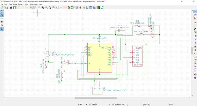
The wires can cross in a schematic, but organization is still important for debugging. The dots represent node, or points where wires are connected
The next step in annotating the schematic. Essentially, component footprints are being added to the schematic symbols for the board design process. To do this, select the Assign PCB footprints to schematic symbols icon in the top toolbar:

A new window will open. Footprint libraries in the left column, the parts being used in the schematic and their respective footprint assignments in the center column, and the last column is for filtered footprints based on whatever search criteria was selected.
Add the footprint assignments for each symbol:

Now that’s completed, a Netlist needs to be generated. Do this by selecting the generate netlist icon in the top toolbar:

Select Generate Netlist and save the file:

Circuit board (Pcbnew)
First, run Pcbnew to start a new board by selecting the icon on the top toolbar:

This will open the Pcbnew design window:

Load the saved Netlist to import the footprints. Do this by selecting the Load netlist icon from the top toolbar:

In the new window, navigate to the netlist file that was previously generated and select it. Select Update PCB:

All of the footprints will be uploaded and the wire connections will be displayed. This is called a rats nest:

Start by defining the size of the board. I did this by switching to the Edge.Cuts layer form the layer manager:

Select the Add graphic lines option from the right toolbar:

Draw the lines, paying attention to the length value on the bottom of the screen:

1.8” x 1.2”
Switch back to the F.Cu layer on the layer manager. Drag a box around all of the footprints and drag them inside the box:

This is how much space that can be used
The parts can be selected and dragged to start the layout. Using the original echo board as a reference, drag the footprints around, trying to untangle the rat nest:

The white lines of the rats nest shows where traces need to be connected. To draw traces (or tracks in KiCad), select the Route tracks icon from the right toolbar:

KiCad will snap to the pads of the footprints. Click and drag the tracks and start connecting the footprints:

After a bit of time and moving things around, a usable board will emerge:

The last thing to do is check the design rules. To do this, select the Perform design rules check icon on the top toolbar:

Fill in the settings based on the design rules and select Run DRC:

The board is complete, a file that can be used to cut needs to be produced.
SVG
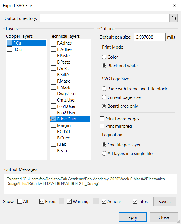
KiCad allows for multiple different types of files to be exported for cutting. I plan on using mods to generate the g-code for the Shopbot, so I need SVG files. This is done by first selecting File=>Export=>SVG. Two files need to be generated, a file for the copper layer, and a file for the edge cut.
For the copper layer, select the F.Cu option in the Copper layers column, and de-select everything in the Technical layers column:

Note the other settings
Fro the edge cuts, de-select everything in the Copper layers column and select only the Edge.Cuts option in the Technical layers column:
These are the resulting outputs converted to .png files:

A second, easier to mill option:

Production


Programming
To program this board, I used an FTDI cable and a serial-UDPI FT230X adapter board.

The adapter board does not provide power, so a second FTDI cable was used on the 6-pin header for power

The code that was uploaded was the attiny412 blink code. Due to the similar architecture of the chips, the 412 code loaded into the 1614.
I modified the code to take advantage of the two LEDS I put into the board, so they alternate blinking
//hello.t412.blink.ino
//
// tiny412 blink hello-world
//
// Neil Gershenfeld 12/8/19
//
// This work may be reproduced, modified, distributed,
// performed, and displayed for any purpose, but must
// acknowledge this project. Copyright is retained and
// must be preserved. The work is provided as is; no
// warranty is provided, and users accept all liability.
//
// Modified by Christopher Leon 4/7/2020
// Alternates between two flashing LEDs using an ATtiny1614

#include <avr/io.h>

#define LED_AVR PIN5_bm
#define LED_ARDUINO 0
#define LED_ARDUINO_1 1

void setup() {
   PORTA.DIRSET = LED_AVR;
   pinMode(LED_ARDUINO,OUTPUT); // does the same thing
   pinMode(LED_ARDUINO_1,OUTPUT);
   }

void loop() {
   //
   // timing tests
   //
   // Arduino digitalWrite: 3.9 us/bit
   //
   digitalWrite(LED_ARDUINO,HIGH);
   digitalWrite(LED_ARDUINO,LOW);
   digitalWrite(LED_ARDUINO_1,HIGH);
   digitalWrite(LED_ARDUINO_1,LOW);
   //
   // port read-modify-write: 304 ns/bit
   //    6 cycles at 20 MHz
   //
   PORTA.OUT |= LED_AVR;
   PORTA.OUT &= ~LED_AVR;
   //
   // port bit write: 96 ns
   //    2 cycles at 20 MHz
   //
   PORTA.OUTSET = LED_AVR;
   PORTA.OUTCLR = LED_AVR;
   //
   // virtual port write: 50 ns
   //    1 cycle at 20 MHz
   //
   VPORTA.OUT |= LED_AVR;
   VPORTA.OUT &= ~LED_AVR;
   //
   // blink
   //
   digitalWrite(LED_ARDUINO,HIGH);
   delay(500);
   digitalWrite(LED_ARDUINO,LOW);
   delay(500);
   digitalWrite(LED_ARDUINO_1,HIGH);
   delay(500);
   digitalWrite(LED_ARDUINO_1,LOW);
   delay(500);
   }
Files

This work is licensed under a Creative Commons Attribution-NonCommercial-ShareAlike 4.0 International License.
-
Suggested by our local instructor/evaluators ↩