W06 - Electronics Design
1. Weekly Assignments ( -> what I did this week )
- Group assignment
Use the test equipment in your lab to observe the operation of a microcontroller circuit board
( -> I tested the Digital Oscilloscope and Digital MultiMeter with the group members. )
- Individual assignment
Redraw the echo hello-world board, add (at least) a button and LED (with current-limiting resistor), check the design rules, make it, test it.
Extra credits: Simulate its operation. Render it.
( -> I made hello-world board adding a button and a LED with current-limiting resistor. Then, I checked the functionality. It worked fine. )
Have you?
Questions from “Fab Academy 2020 Assignments and Assessment 
( -> my answers )
-
Shown your process using words/images/screenshots ( -> yes )
-
Explained problems and how you fixed them, including how you worked with design rules for milling (DRC in EagleCad and KiCad) ( -> yes )
-
Included original design files (Eagle, KiCad, Inkscape, .cad - whatever) ( -> yes )
2. Group Assignment Link
I summarized how to use Digital Oscillosope ( Tektronix TBS 1052B ).
3. Works, steps and some details
1) Redraw the echo-world board on EAGLE CAD
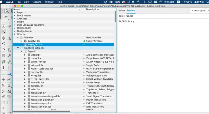
I decided to add one LED and one button.
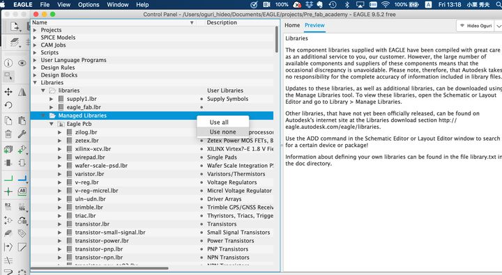
| selected “eagle_fab_lbr” | “Use none” for “Managed Libraries” |
|---|---|
 |
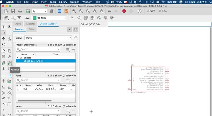
 |
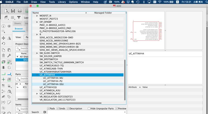
| add parts | selected ATTiny44 |
|---|---|
 |
 |
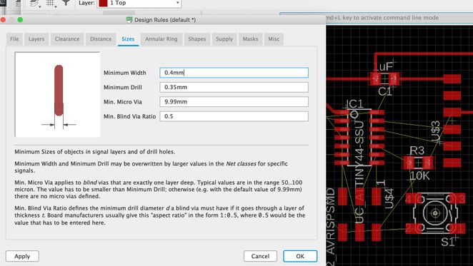
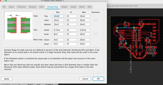
| “design Rules” setting | “Grid” setting |
|---|---|
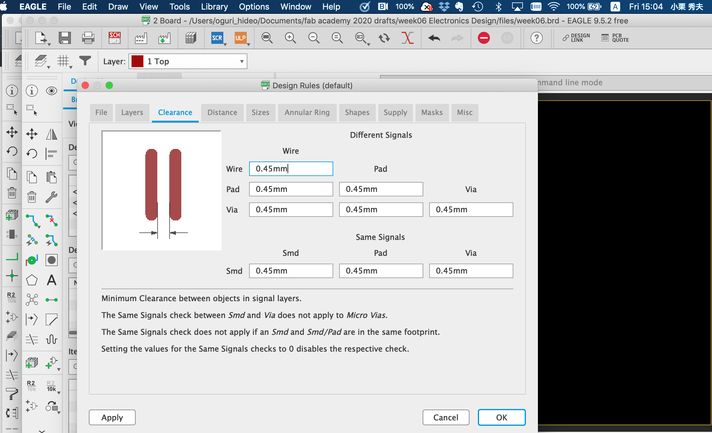 |
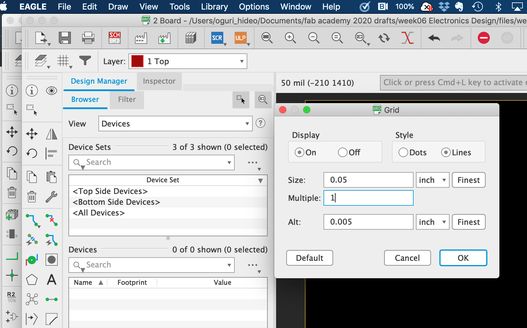 |
| line width setting | ERC error |
|---|---|
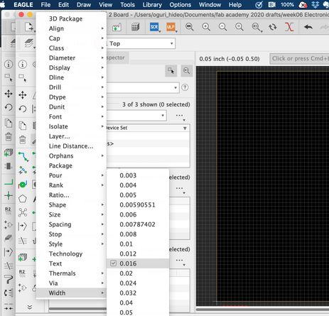 |
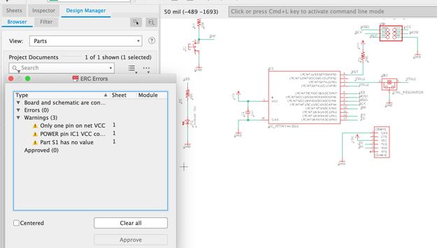 |
| ERC error , and then, fixed one by one | component layout on PCB |
|---|---|
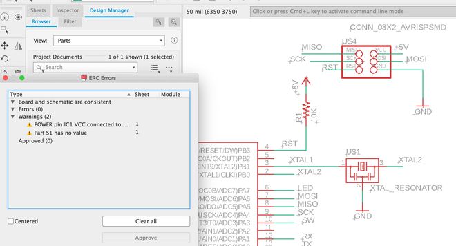 |
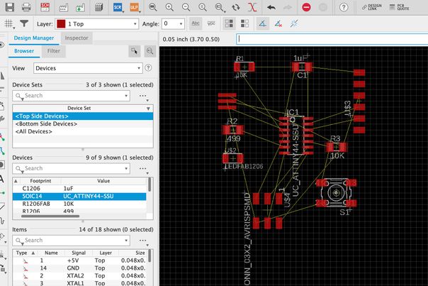 |
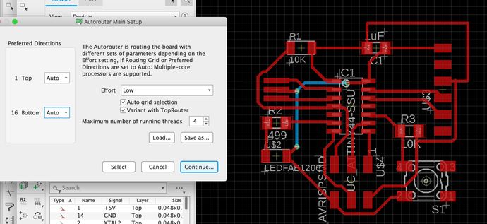
| design Rules | tried “Autoruler” jumper on the backside of PCB is shown with green color |
|---|---|
 |
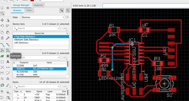 |
| “Autoruler” setting | “Autoruler” setting ( this was used ) |
|---|---|
 |
 |
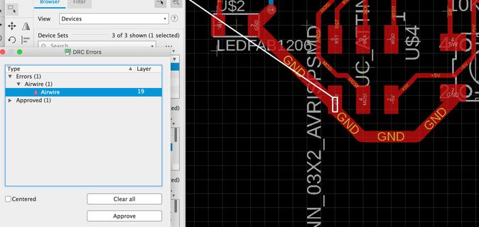
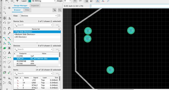
| After thickened GND lines manually, DRC error ( airwire ) were found, but not a big problem | blue line shows the jumper on the backside of PCB, so tried to set the holes and via |
|---|---|
 |
 |
| relocated the route of jumper so that it can be soldered firmly. | hole diameter |
|---|---|
 |
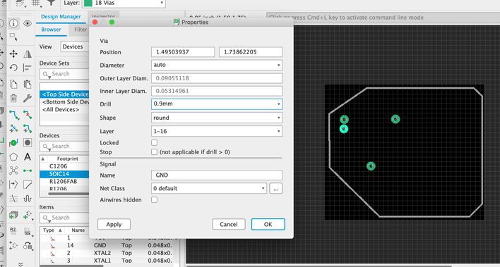 |
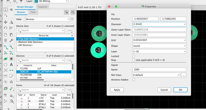
| “via” ( to support jumper ) property | |
|---|---|
 |
 |
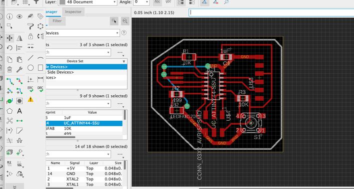
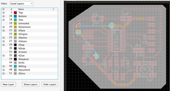
| design completed | |
|---|---|
 |
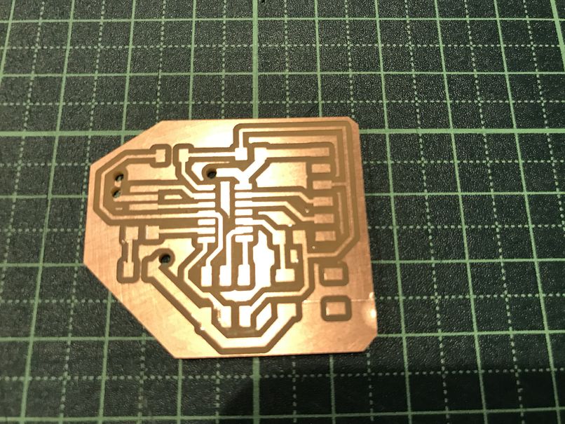
2) Milling PCB and Stuffing
CNC parmeters for circuit pattern
tool diameter (in) ; 0.0156 (1/64)
cut depth (in) ; 0.004
max depth (in) ; 0.004
offset number ; 4
milling speed ; 4 mm/s
| mods to create the circuit pattern ( “dpi” needed to be changed from 800 to 1600, to fit the proper scale. This might be depending on the MacBook Retina display. ) | |
|---|---|
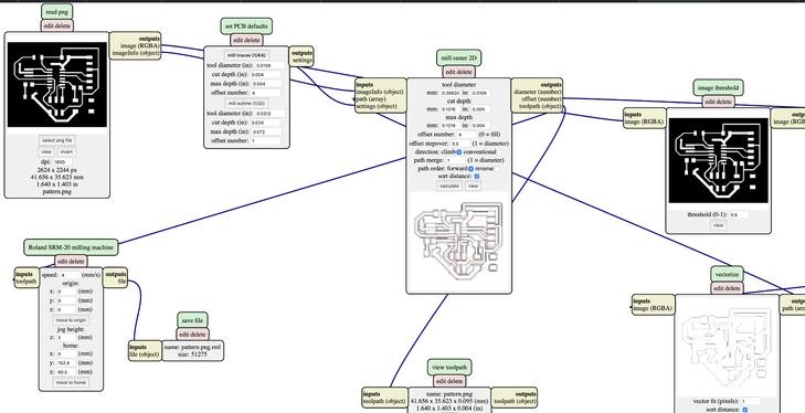 |
CNC parmeters for holes and outline
tool diameter (in) ; 0.0312 (1/32)
cut depth (in) ; 0.024
max depth (in) ; 0.072
offset number ; 1
milling speed ; 4 mm/s
| mods to create the holes ( also, “dpi” 800 -> 1600 ) | |
|---|---|
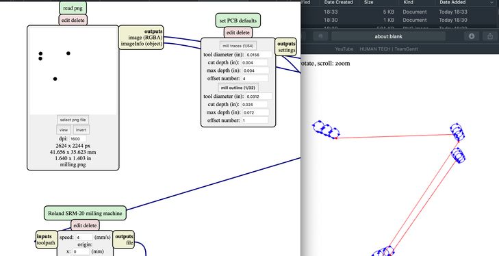 |
| pattern.png | jumper holes ( milling.png ) |
|---|---|
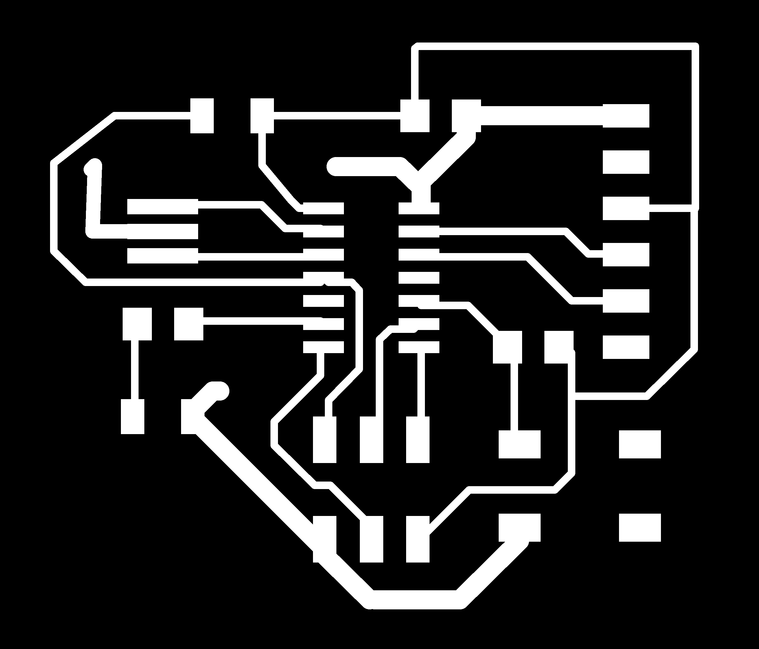 |
 |
| milling the plate | |
|---|---|
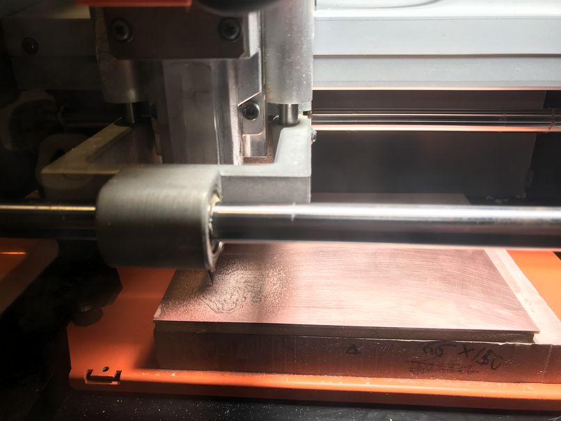 |
| unnecessary portions were removed | |
|---|---|
 |
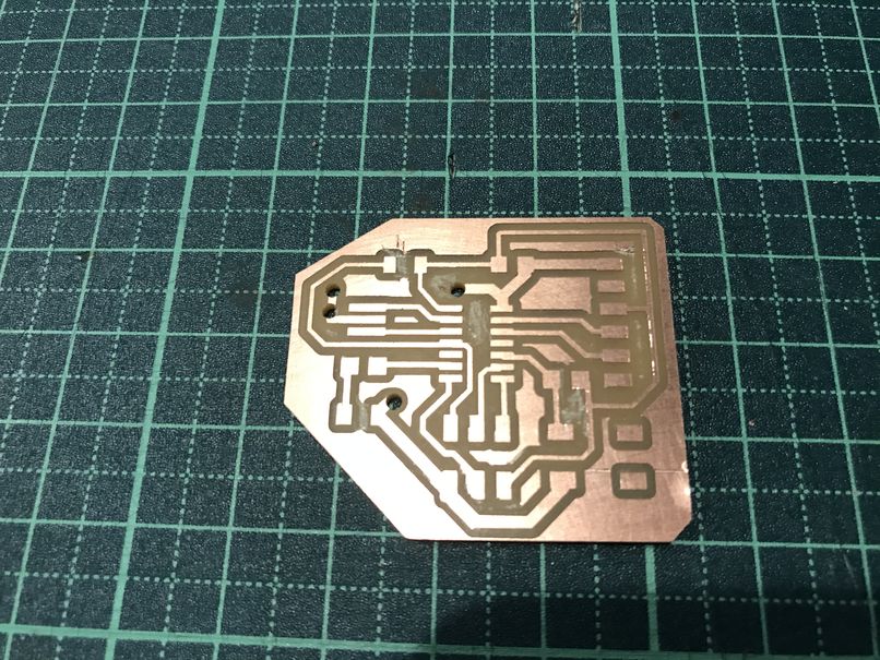 |
| after stuffing the components ( added the black mark for GND ) |
jumper, backside |
|---|---|
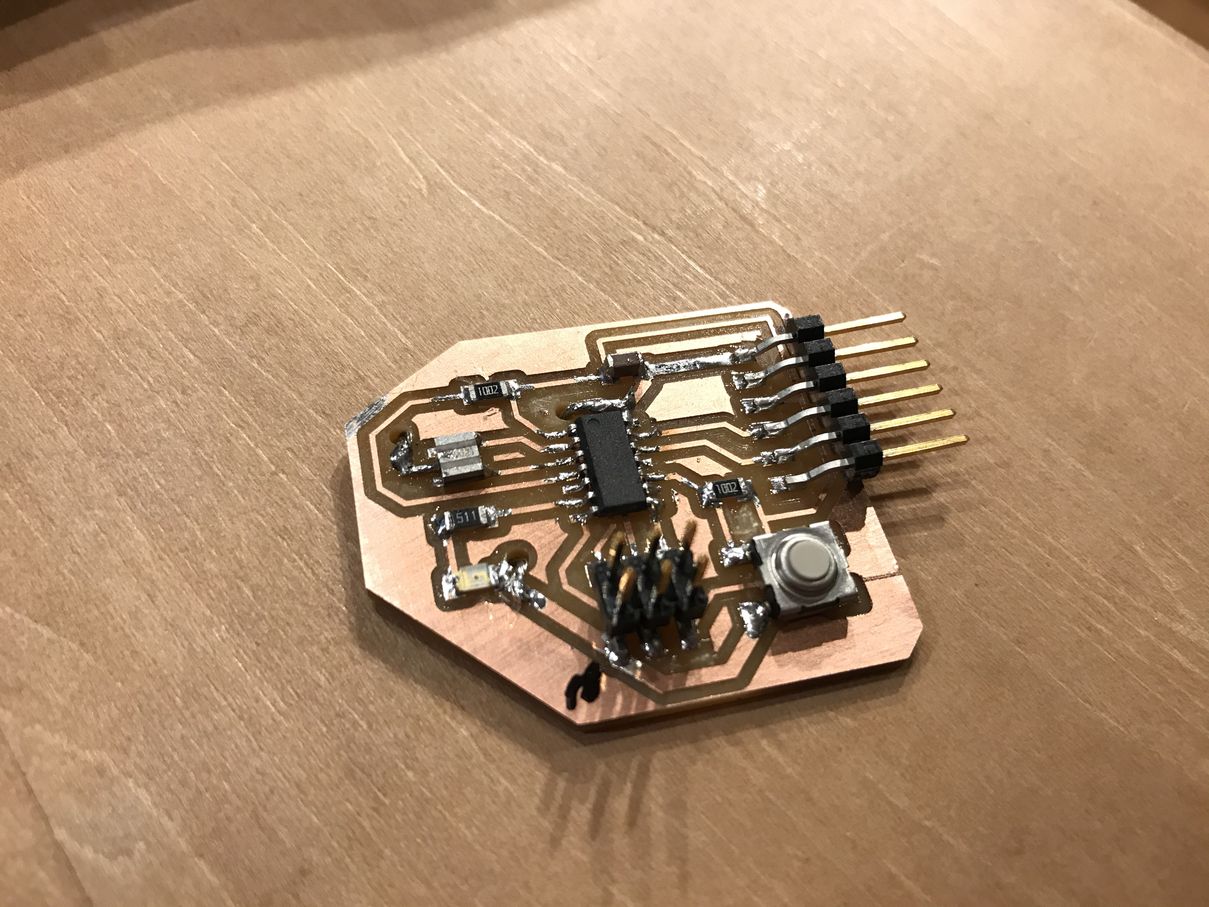 |
 |
3) Functional Check
A. echo program
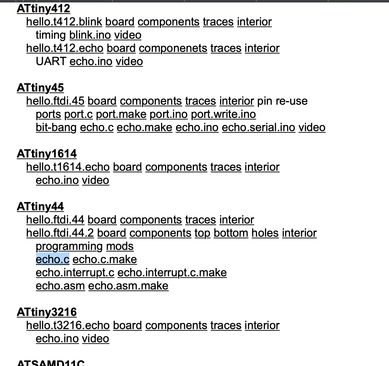
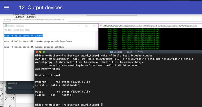
I downloaded “hello.ftdi.44.echo.c” from fab academy site, and implemented using the commands below, referring the site below.
12. Output devices : fab academy 2019 Rico Kanthatham
make -f hello.ftdi.44.echo.c.make
make -f hello.ftdi.44.echo.c.make program-usbtiny-fuses
make -f hello.ftdi.44.echo.c.make program-usbtiny
| downloading “hello.ftdi.44.echo.c” | implementation |
|---|---|
 |
 |
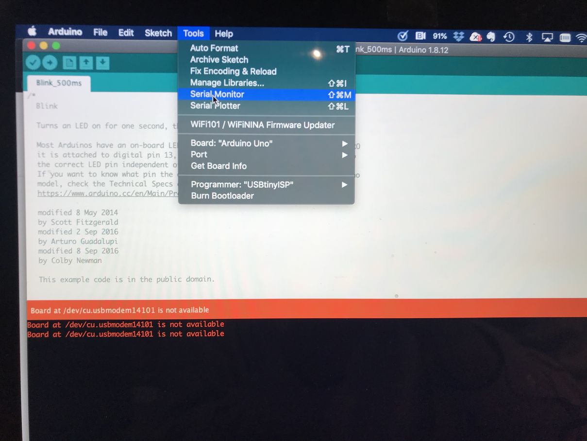
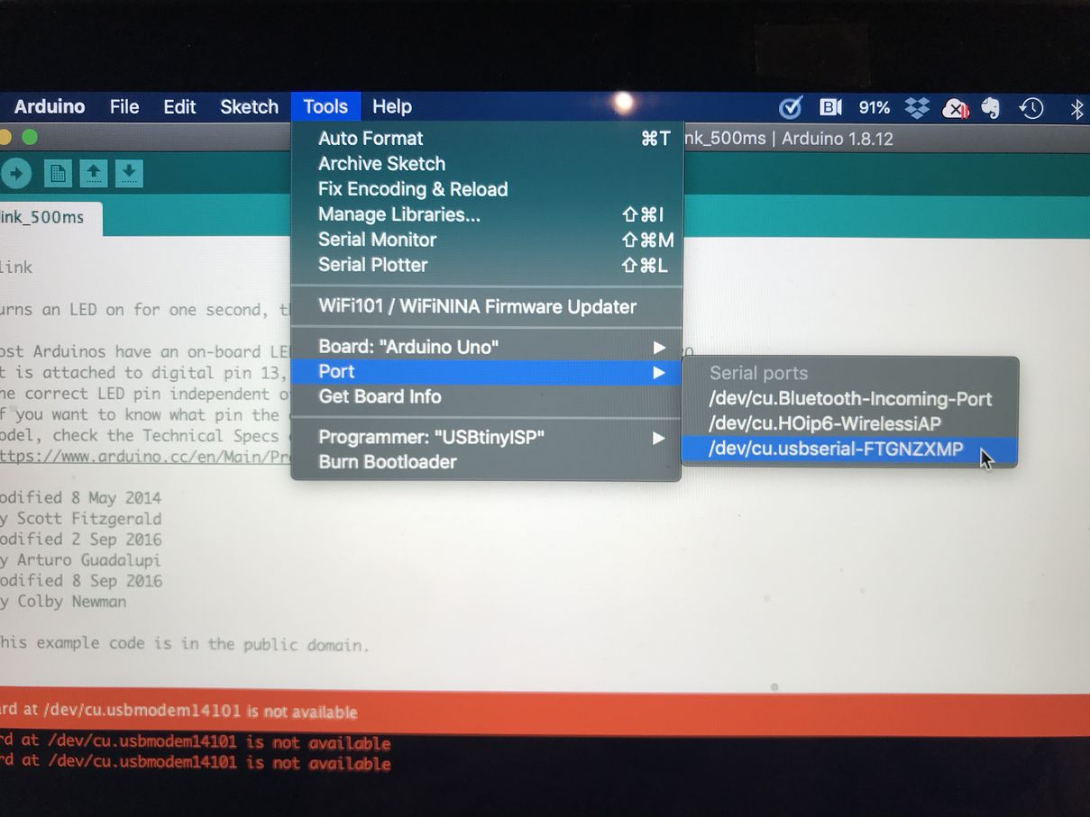
| selected “Serial Monitor” in Arduino IDE | port setting |
|---|---|
 |
 |
| 115200 baud rate | It worked fine! ( but put PCB on the aluminum body of MacBook might “not” be a good idea ) |
|---|---|
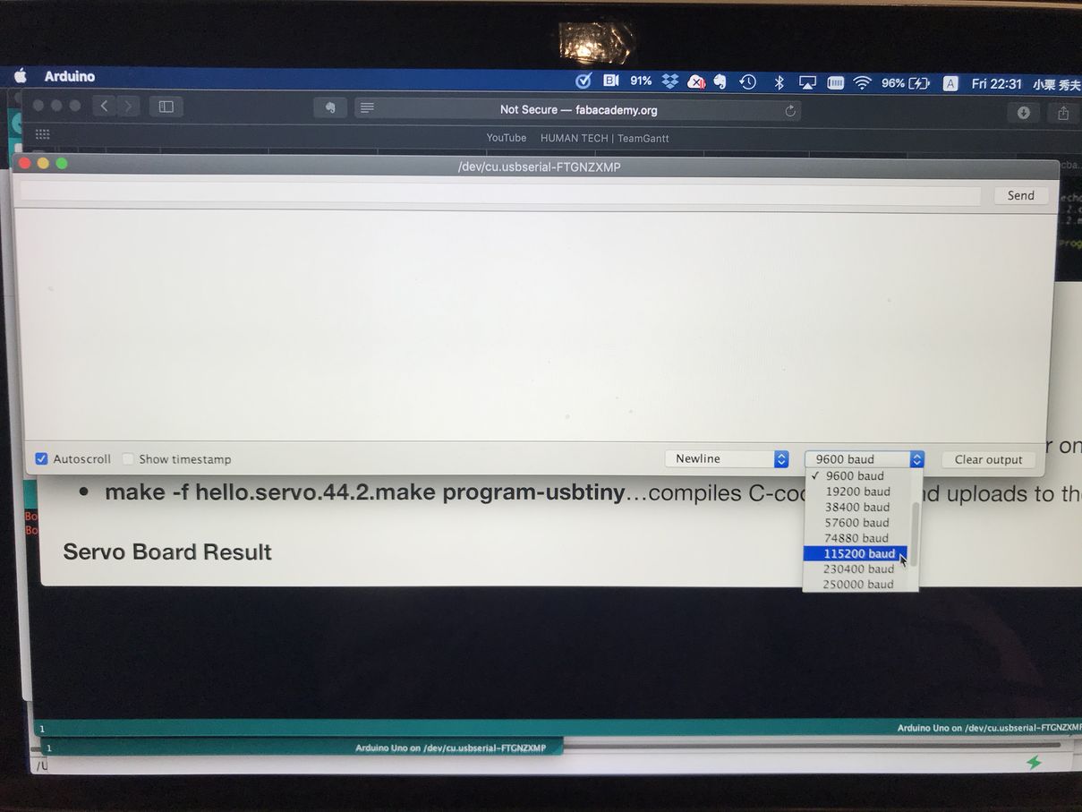 |
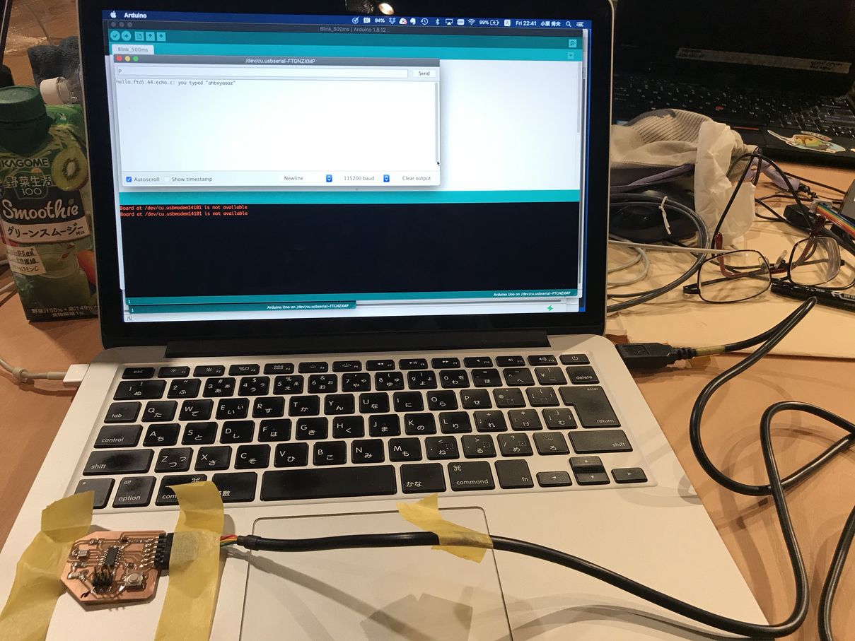 |
| LED on-off switching test | |
|---|---|
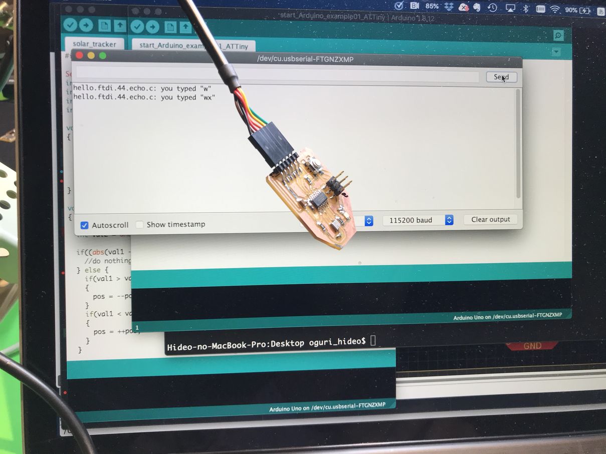 |
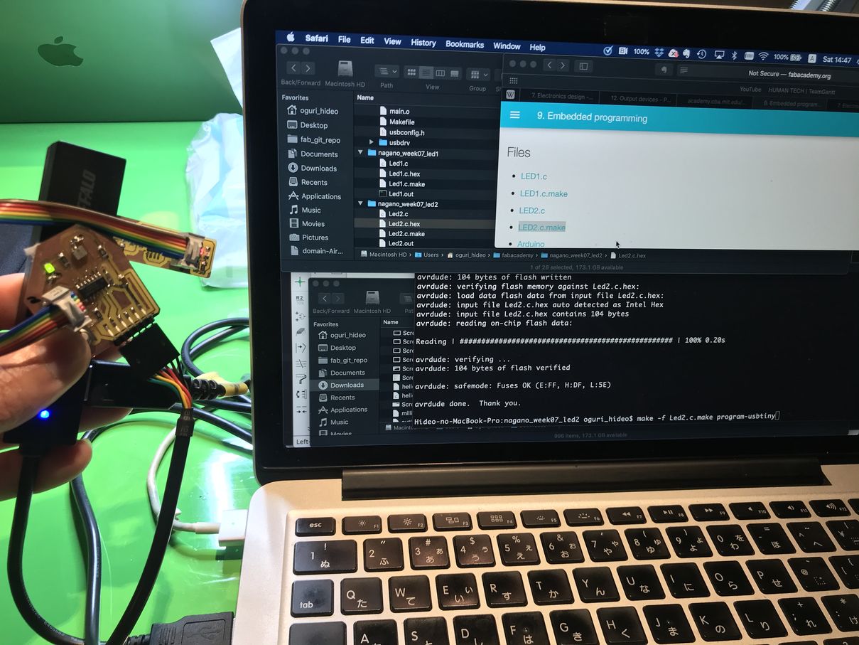 |
B. LED on-off switching program
I downloaded and implemented the program file “LED2.c” from the site below.
And, it worked fine.
9. Embedded programming : fab academy 2019 Kae Nagano
4. Important Learning Outcome
1) GND design on PCB
In order to avoid the possible problems regarding the ground lines on PCB, I decided to use jumper on the backside of PCB, also manually thickened the GND lines.
The PCB worked fine, although whether it was because of the above decision or not, I think this is a safer way especially for more complicated PCB design.
2) EAGLE “Autoruler”
This function helped me a lot to save time. I’ll explore this function more precisely.
5. Links to Files and Code
EAGLE CAD files :
week06.sch download
week06.brd download
.png files :
pattern.png download
milling.png download
outline.png download
.rml files :
pattern.png.rml download
milling.png.rml download
outline.png.rml download
“echo hello” files :
hello.ftdi.44.echo.c download
hello.ftdi.44.echo.c.make download