5. Electronics production
1.Highlights of the week
2. Group Assignment
We characterised the design rules for our PCB production process.
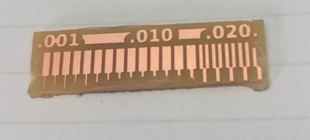
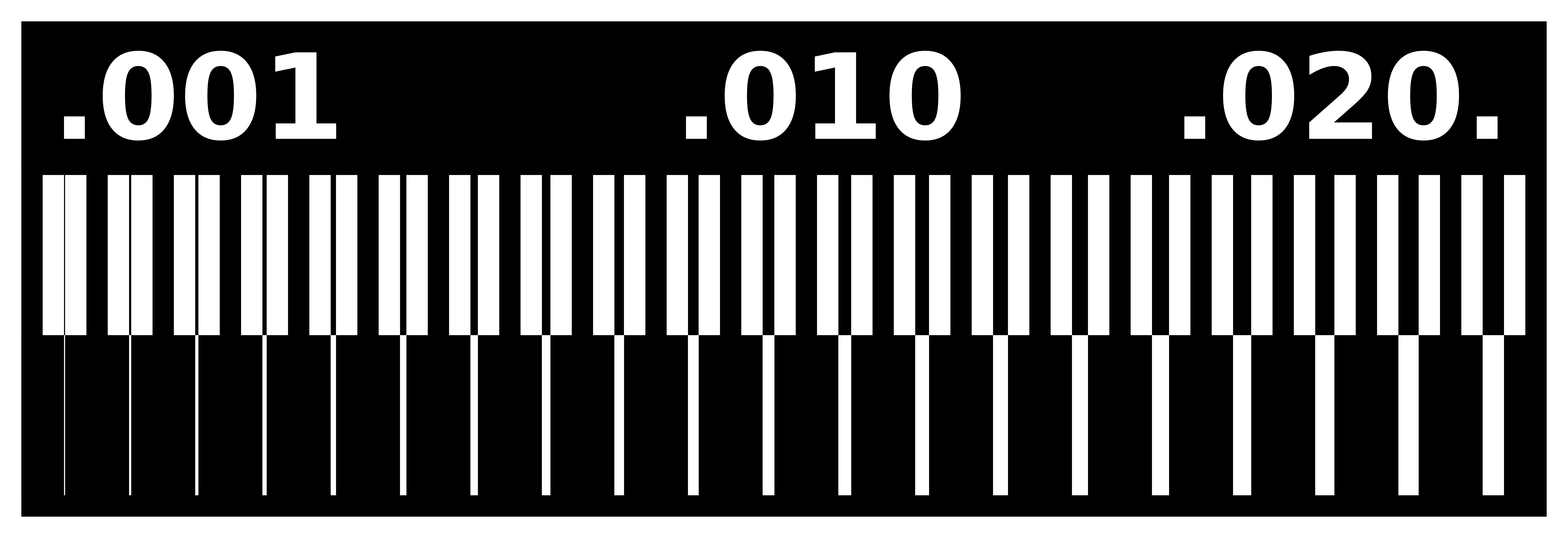
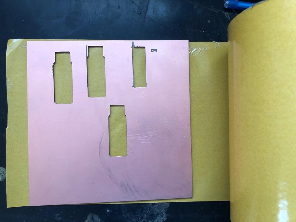
Line Test: Manoj Sahukar and me teamed up for the assignment.
A. The line test images were taken from Fab Academy Electronics Syllabus.
 B. We used FabModules to generate .rml files. Various other settings like process,speed,X,Y,Z coordinates were entered.
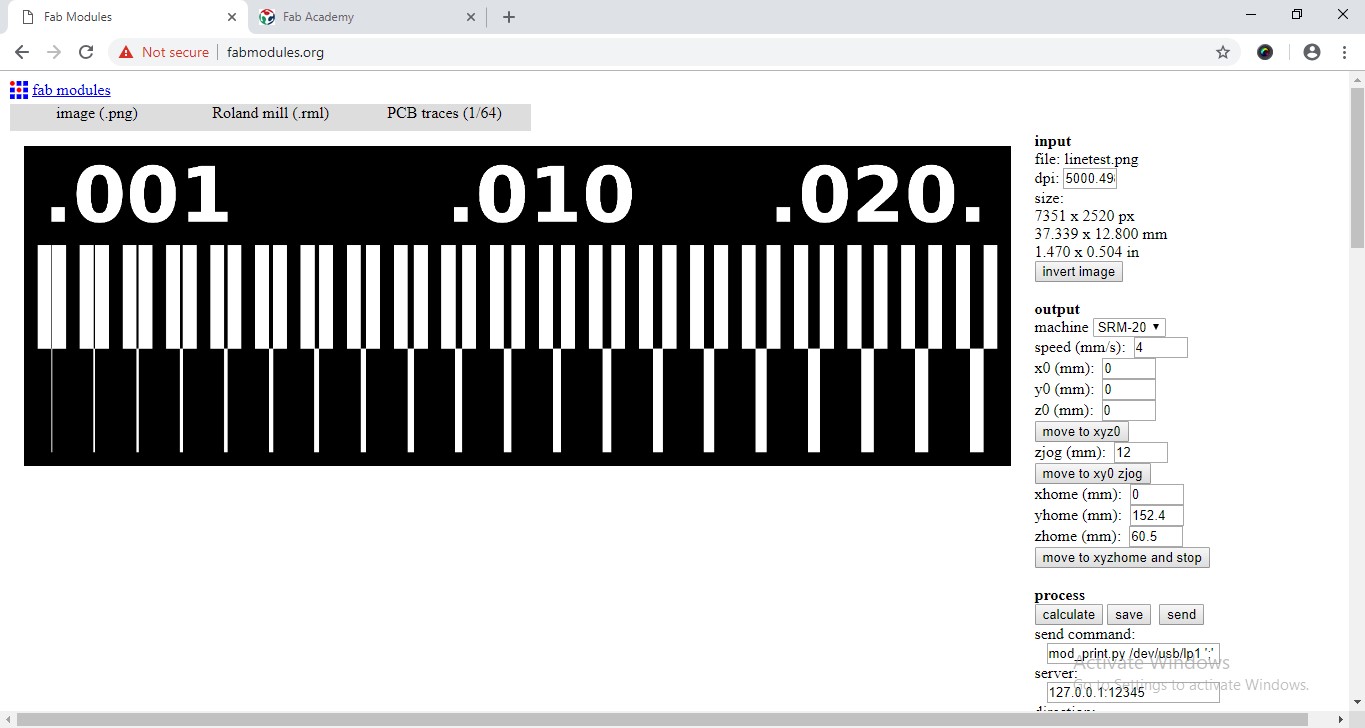
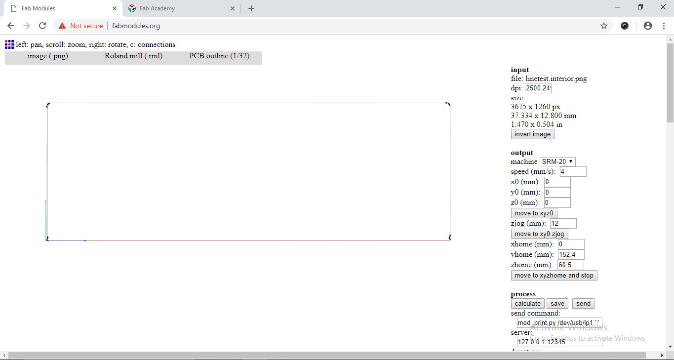
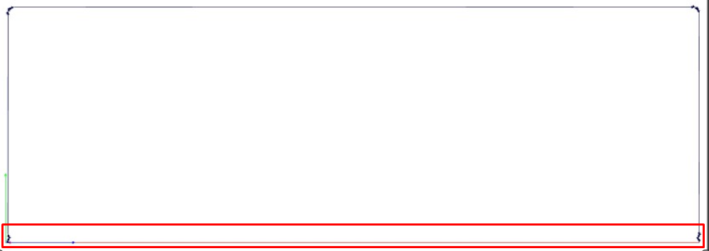
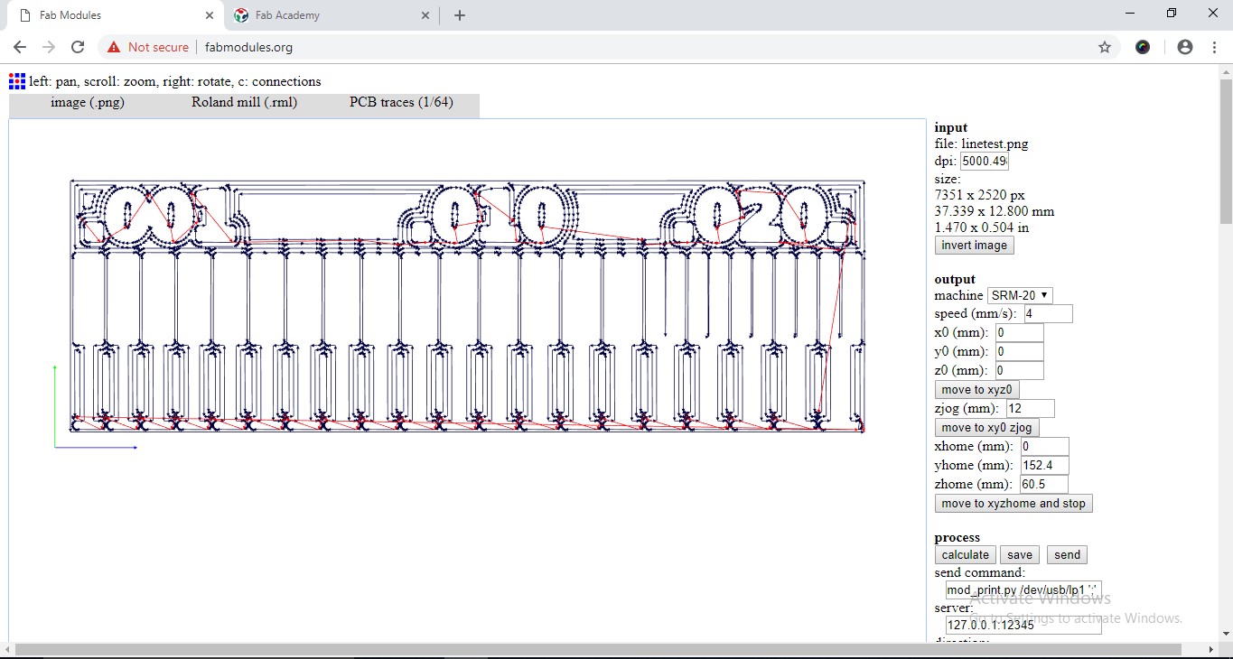 C. There was 1 line of the reactangle Red which showed jog path. The FabModule didn’t create close rectangle which can be seen in the picture below.
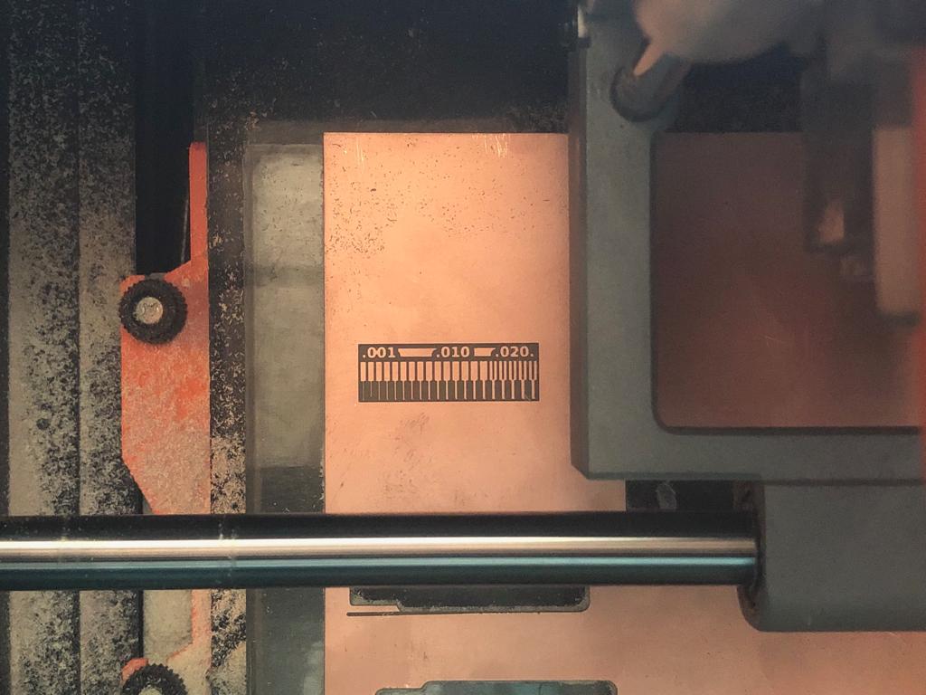
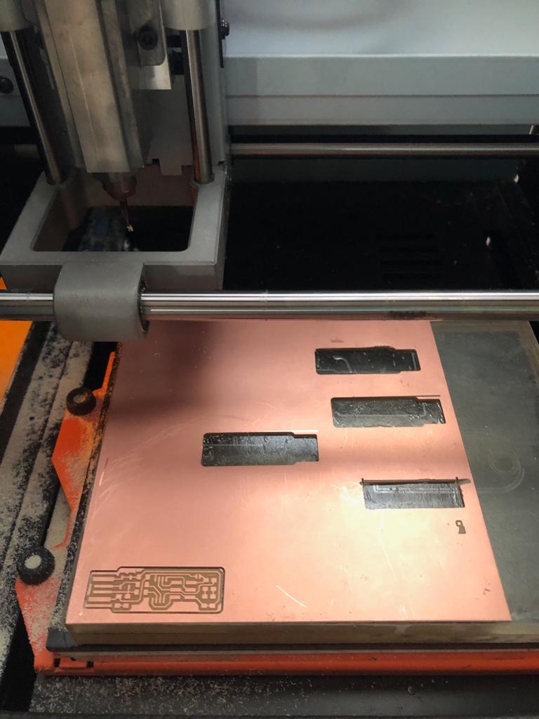
 D. We cut the board on SRM-20 machine. Gave 2 commands to trace the lines of various thickness and cut the outline.
E.Conclusion:
1. The board showed the smallest thickness line was cut prperly. Thus, giving green signal for the tracing and outline ahead.
F. Problem:
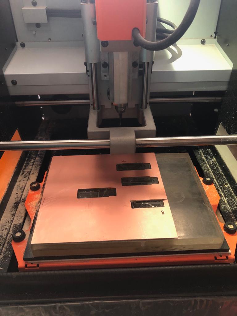
The board wasn’t cut from one side because the path only showed way for 3 sides of the rectangle. Though the input image(.png) had a close rectangle, on FabModules in path 1 line of the rectangle was Red and showed jog path.
 To fix this problem, we cut the 4th side of the board with grinding machine. This damaged the board little bit yet the test part was clearly visible.
We also reversed the rectangle outline design to get path on the 4th side and again calculated the path. Yet fab modules gave the same result showing the same 3 sides for cutting. Moreover, during the lecture we realised the same problem of machine not cutting the 4th side of the rectanagle was also faced by other labs. Yet the assignment was done successfully as the traces were clearly visible.
3. Individual Assignment
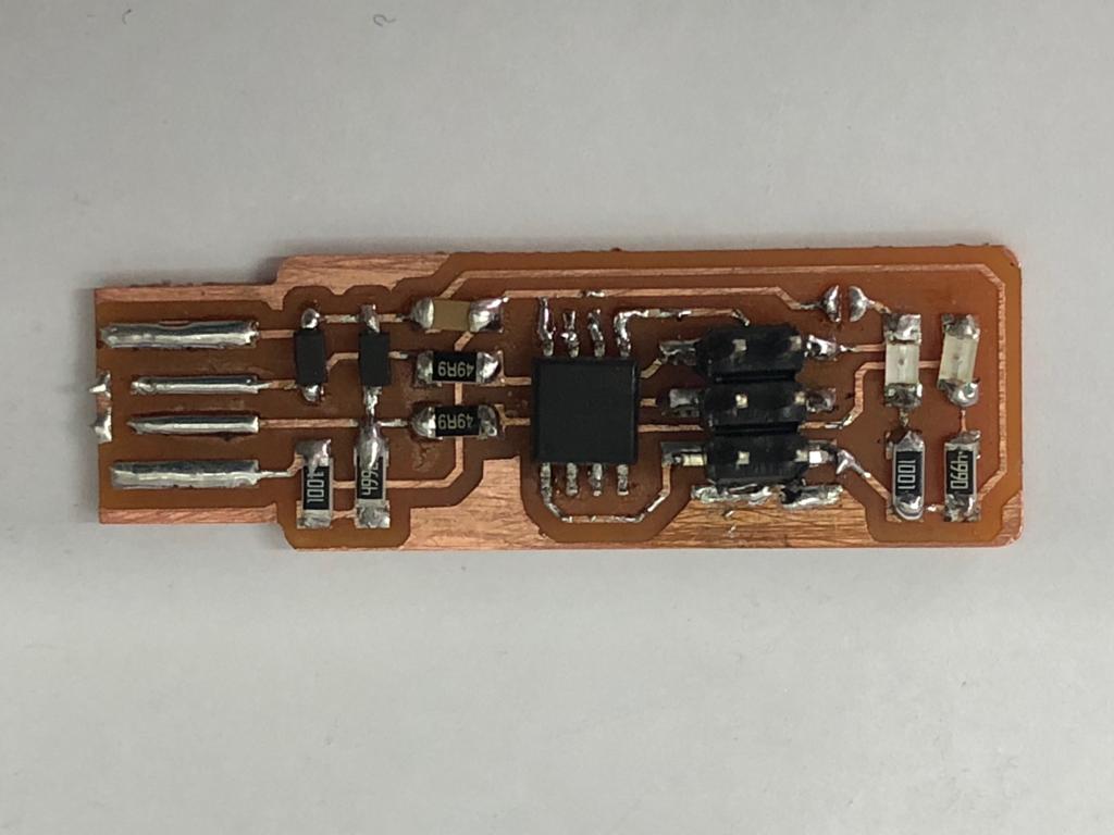
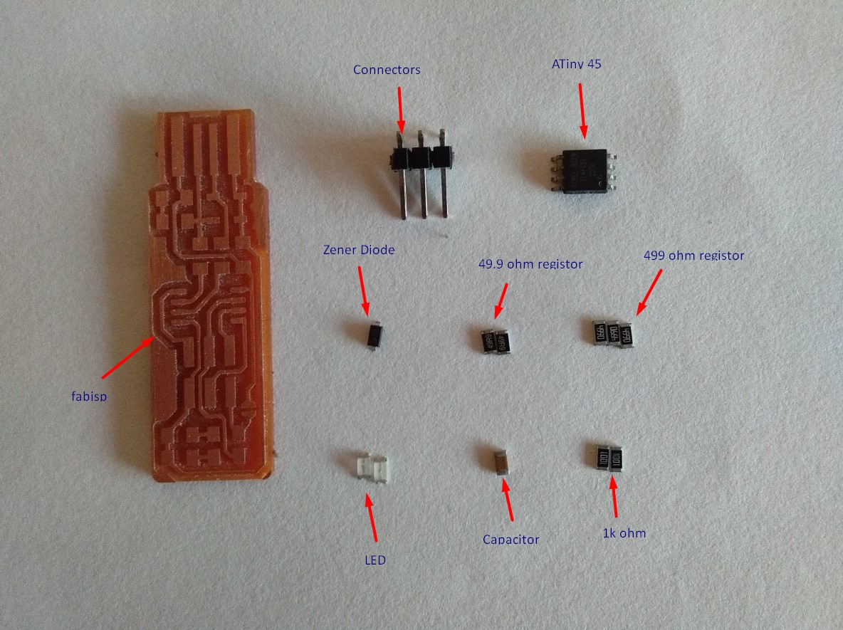
I made an in-circuit programmer by milling the PCB using SRM-20 and programmed it.
I have used Brian example for refernce.
3.1 Files from Brian
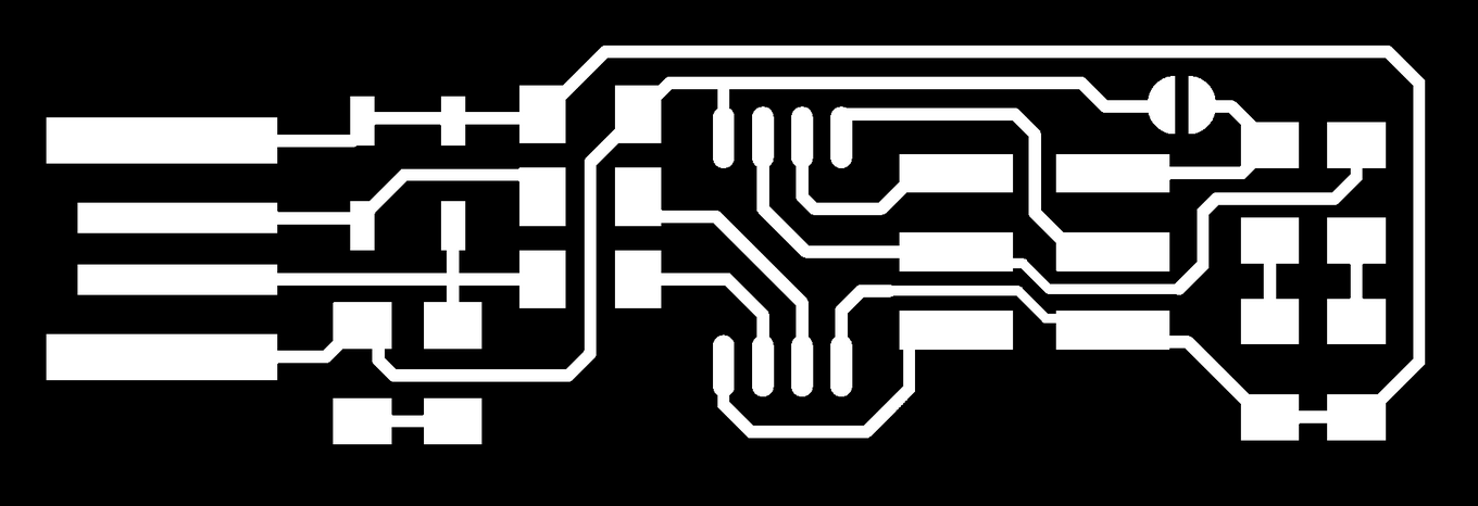
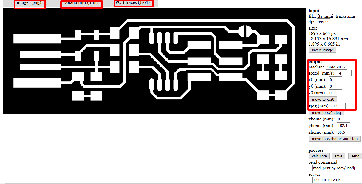
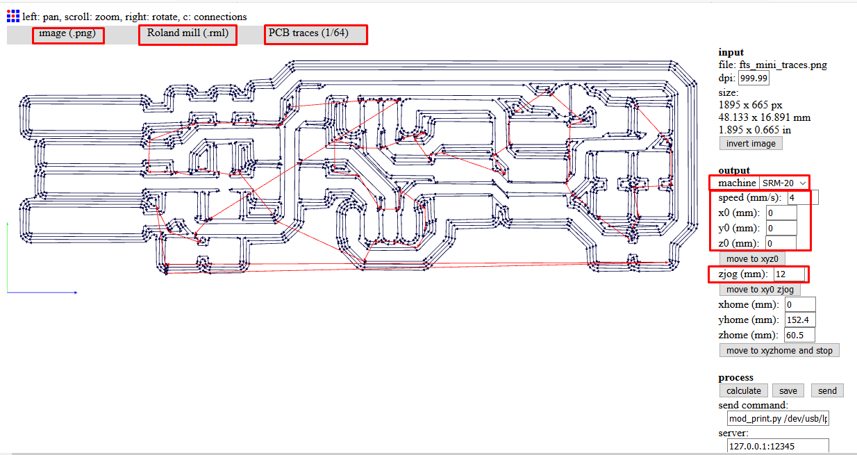
“Traces” and “Outline Cut” files in png format of 1000 dpi were downloaded from Brian

3.2 Fab modules
I used Fab modules to change the settings and format of the png file. The instructions added were:
A.Input file:selected image(.png) formate because the file in the local sysetm is in png format. Other input formats of drawing(.svg),mesh(.stl),volume(.vol) can also be converted.
B.Output file:Roland mill(.rml) is the desired format of the output file because .rml is supported by SRM-20.Yet otherwise files can be converted to G-codes(.nc),Roland Vinyl(.camm),Shopbot(.sbp) etc.
C.Process:for engraving/traces seleced “PCB traces 1/64” and for cutting “PCB outline 1/32”. Other processes which Fab modules support are rough and finish wax cut.
D.Machine:SRM-20 is the machine used for milling.Other machines in options are MDX-15,MDX-20 and MDX-40.
E.X,Y,Z axis: all 3 values were adjusted to “0 mm”.The starting coordinates of end mill can be adjusted from here too.
F.Speed: “4mm/s” for both the processes traces and outline.This is the speed at which end mill will move for the process.
G.zjog: It is basically the distance of z axis when end mill moves to mill from one part of the design to other. I fixed the value as 12mm.
H. Offset:The number of turns of endmill for making trace/track. This setting majorely affects on the final product. Paths that are not cut in the first pass post probably will be cut during the other passes. So, more the offset cleaner the board and less the offset will have broad traces and very tricky to solder it. Also board looks dirty.
I.Calculate: This showed the “path” of the end mill in “Red lines” on the file design.
J.Save: The file was finally “saved in .rml format” and ready for milling.
3.3 SRM-20 Machine & Software
A.Placed sacrifical layer and cleaned: I used acetone to clean the surface. The width of the acrylic sacrifical layer at our lab is 21 cm. Smooth and uniform surface is vital which decreased the chances of bid getting damaged.
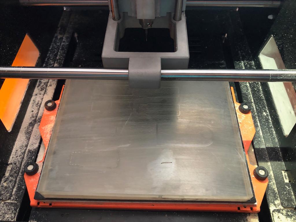 B.Sticked FR1 board to sacrifical layer: Double side tape sticked on the bottom of the FR1 board and I sticked it on the sacrifical layer.
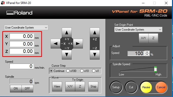
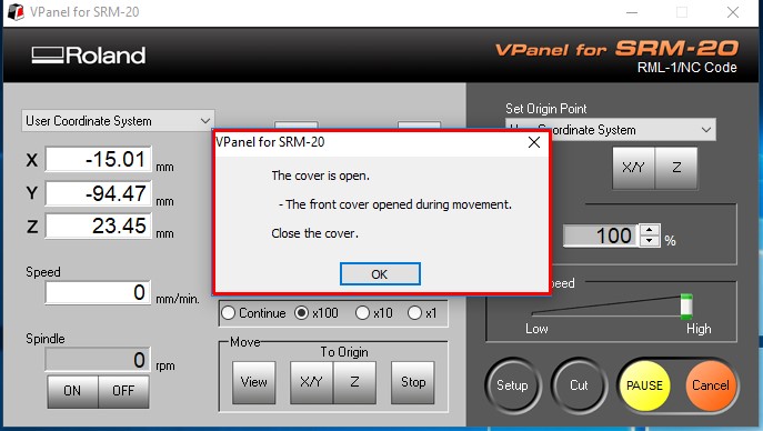
 C. V Panel software & Machening:The sofware gives us the access to set origin, adjust axis and give command to the machine.
a.Adjusted X&Y axis:Under user coordinate system and looking at the space on the FR1 board set the origin.
b.End Mill in Collate:Inserted the end mill in the collate and moved to the set X,Y origin. Here, I set the collate loose and allowed the end mill to touch the board.
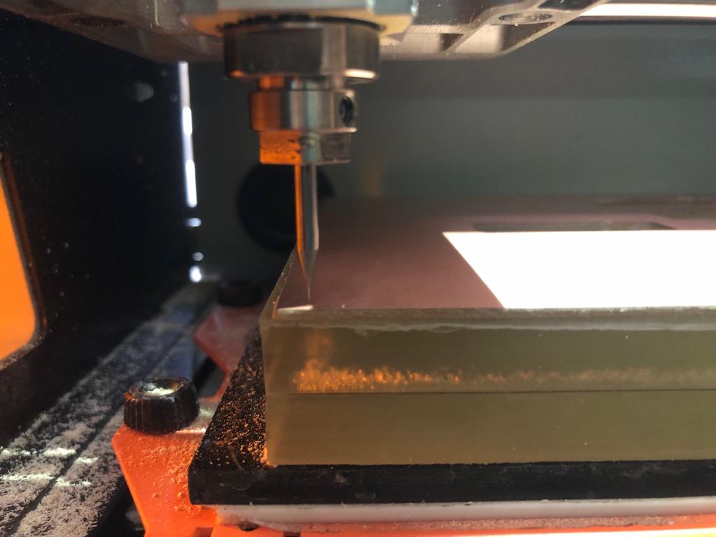 c.Z azis:After tightening the collate this fixed position was marked as origin for Z axis.
d.Setup & Tracing:Under setup command the file was sent to the machine and it started tracing.
e.Opearation: The end mill moved and traced the board. The speed and spnidle value was visible on the software.
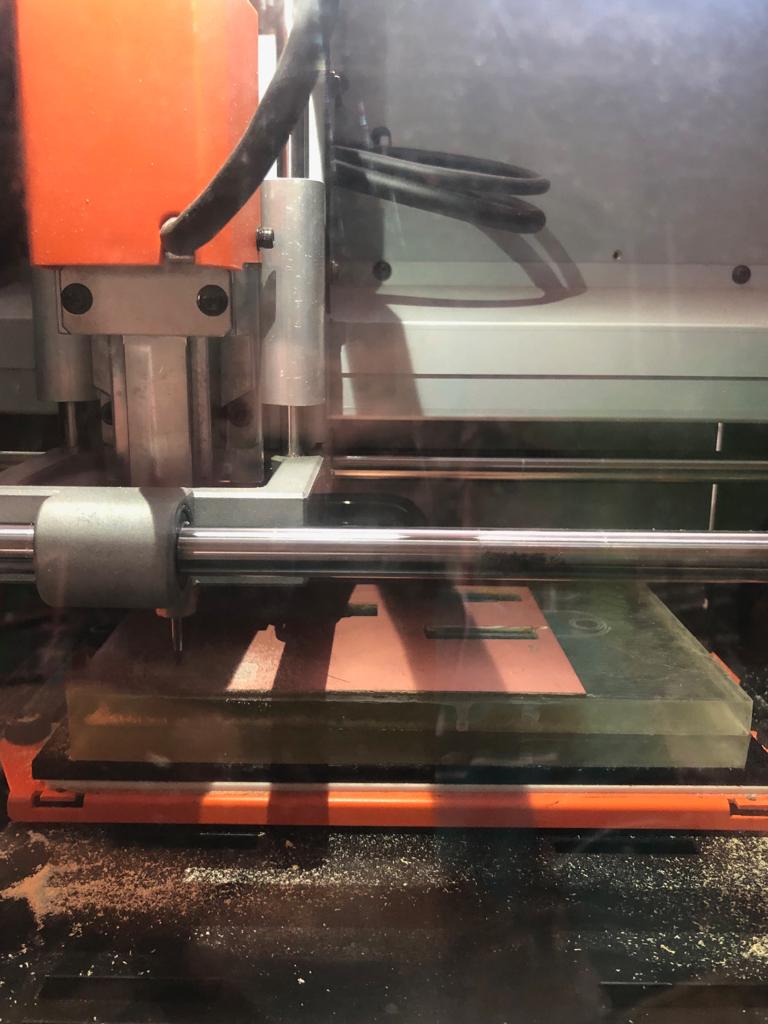 f.Changed end mill:The end mill was changed from 1/64 to 1/32 for cutting the outline. I followed the same commands keeping the X,Y origin positions constant.The Z origin was marked again because the position may have slightly shifted while changing the end mill.
 g.Operation:This time to cut the board the end mill went deeper showing the value in display. Machine stopped on completing the instruction and I removed on the PCB board from the sheet.
3.4 Soldering
A.Sand Paper:I scrubbed the PCB board with sand paper. This made the surface rough and easy for filler to stay on the board.
B.Components of circuit:
a. 1x ATtiny45 or ATtiny85
b. 2x 1kΩ resistors
c. 2x 499Ω resistors
d. 2x 49Ω resistors
e. 2x 3.3v zener diodes
f. 1x red LED
g. 1x green LED
h. 1x 100nF capacitor
i. 1x 2x3 pin header
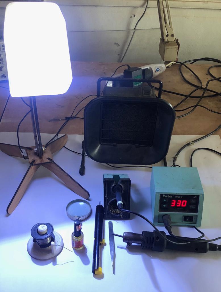
 C.Equipemnts used for soldering:
a.Filler: The wire melted in contact with soldering iron and dried immediately when placed on the PCB board. This conducting material fixed board and components.
b.Flux:The chemical fecilitated the soldering process. I tried both liquid and solid flux.
c.Soldering Iron Rod: Used the rod at 330°C to melt the filler and place it between components and board.Placed the rod in the stand when not in use.
d.Hot Air Gun: The air at very high melted the filler instantly. The equipment was handy during desoldering.
e.Exhaust Fan: On melting filler gases were liberated which were pulled away by the fan.
f.Desolder Pump:The pump sucked the filler and helped removing the components from the board.
g.Twisers:To pick and place the components the twisers were very hrlpful.
h.Magnifying Glass: The components are marked but the words written are very small.Used maginifying glass to read the specifications mentioned on components.
i.Light lamp:The light helped identifying small components of the circuit and the gaps to solder.
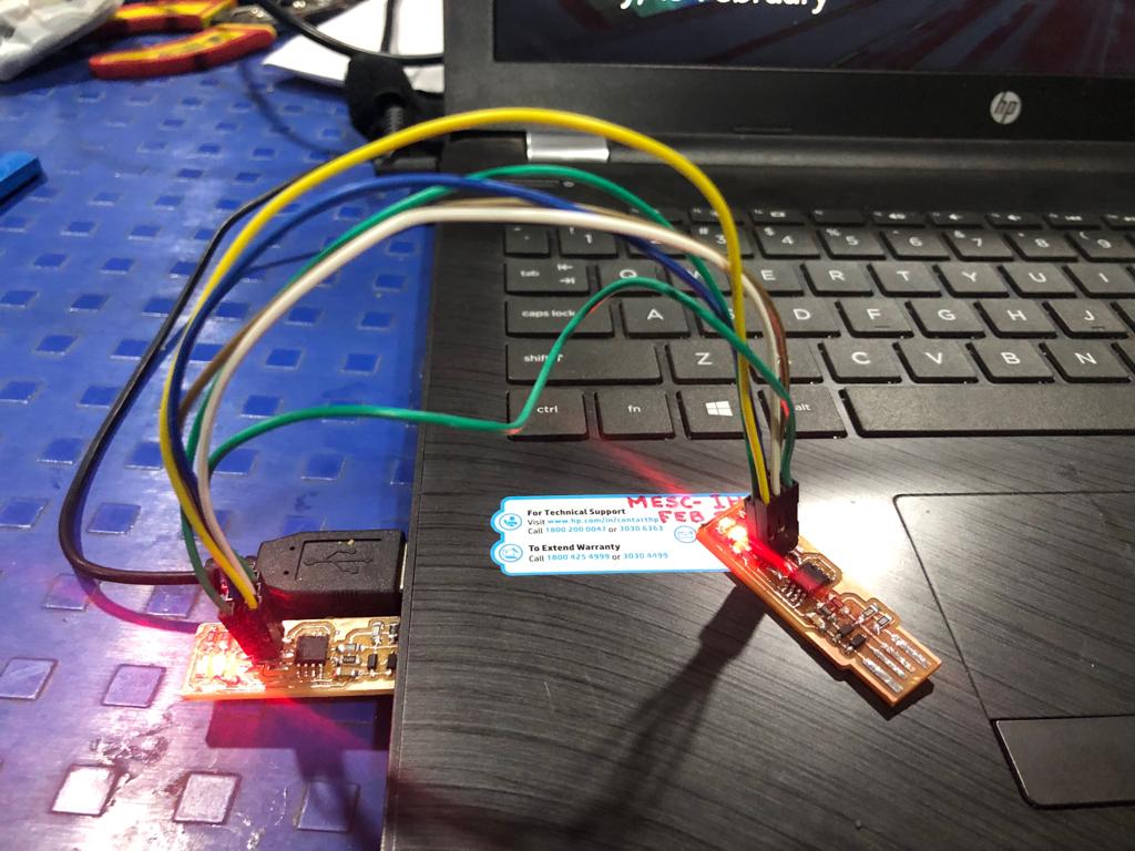
D.Fixing and Handling:Referred the diagram from Brian and placed the above components to solder the PCB board:
3.5 Checked Circuit
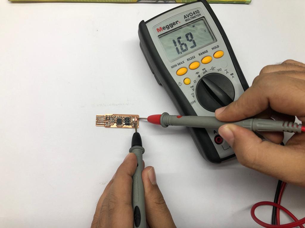
I used multimeter to check the connectivty across all the parts. Using cathode and anode of multimeter to diodes,capacitor, LEDs,resisors,Integrated circuit(I.C) ends checked connections at major ends.
3.6 Software Installation
I have used GNU AVR Toolchain for Windows 10
software.
A.Atmel: Downloaded the Atmel Toolchain from Atmel’s site and run the installer.Extracted the files in C:\Program Files.
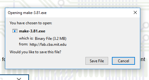
B.Installed GNU Make: Downloaded Gnu Make and installed it in default location.
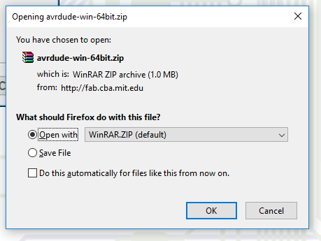
C. Installed AVR dude:Extracted the file in C:\Program Files.
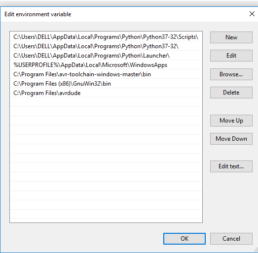
D.Updated Path:
a.Opened the Path setting in the local system:Control Home Panel>System> Advanced system settings> Environment Variables>Path
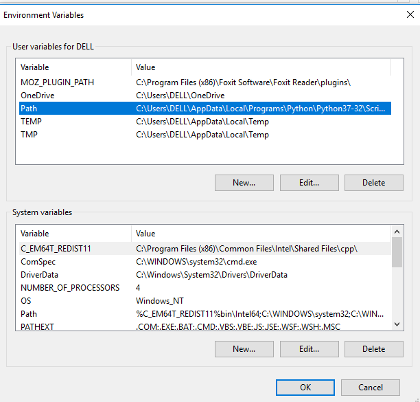
b.Edited Path to add the below 3 values:
C:\Program Files\avr8-gnu-toolchain\bin
C:\Program Files (x86)\GnuWin32\bin
C:\Program Files\avrdude
3.7 Programming
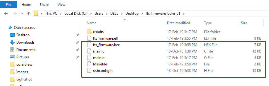
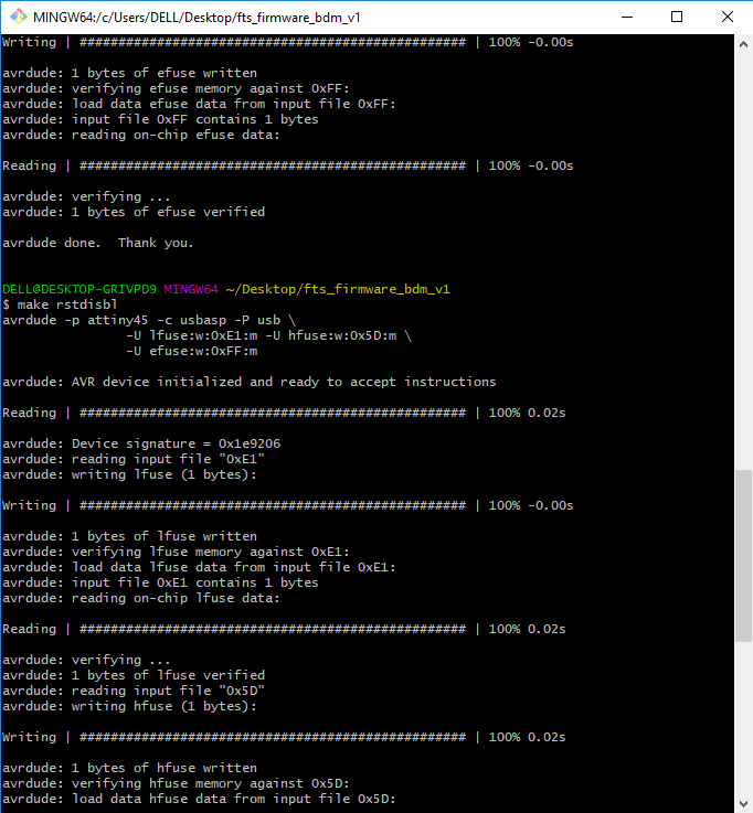
A.Filmware source code: Downloaded and extracted it.Used the command Run make in Git Bash. On completion a new file was added fts_firmware.hex.
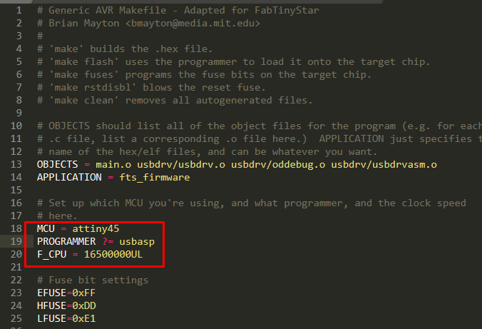
 B.Edited the MAKEFILE: I used Sublime Text to edit. The Makefile, by default, assumes that we will use a programmer in the usbtiny family which I edited to usbasp.
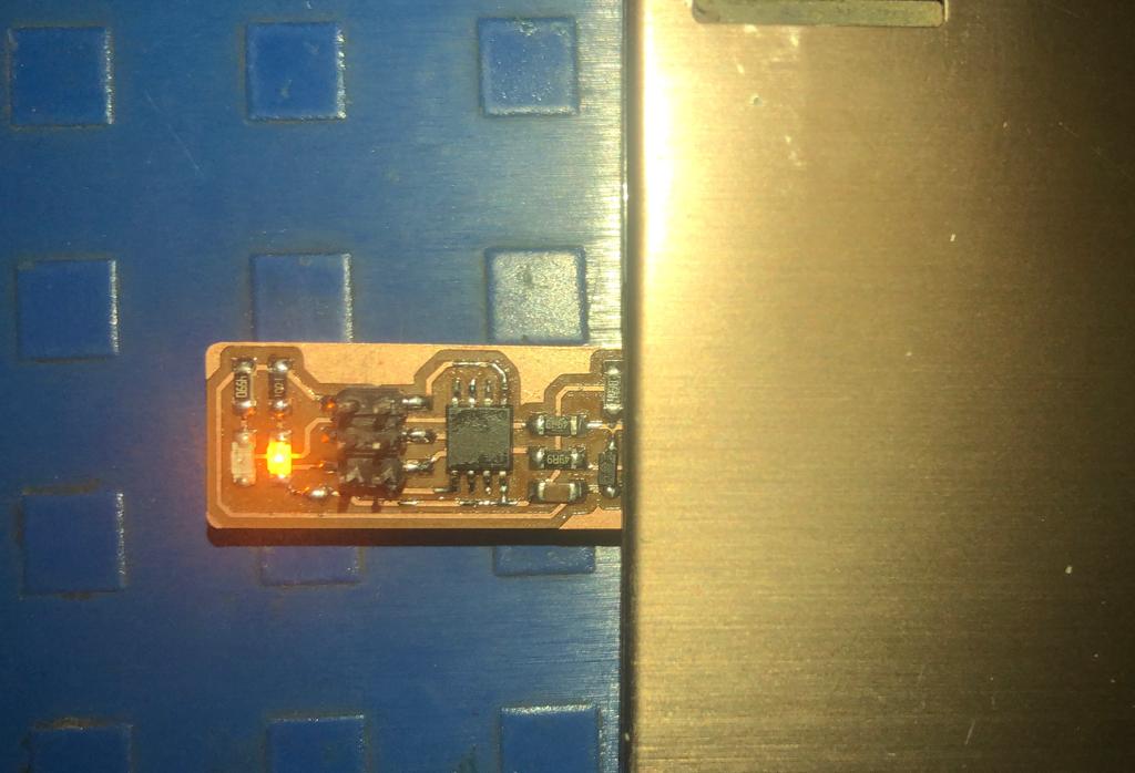
 C.Pluuged the PCB board: Red LED lit on plugging the board in laptop port.The solder jumper was bridged which allowed LED to be the part of the connectivity.
 D. Programmer:Connected the programmer to the ISP header on my board. I was careful while selecting MISO,VPROG,SCK,MOSI,RST and GND such that same wire is connected in ISP header and the programmer.
E.Run make flash: This erased the target chip, and programmed its flash memory with the contents of the .hex file built before.
 F.Final Check:Plugged the board in my laptop USB and it detected the external drive.
G.Run rstdisbl:I connected the ISP programmer board again and gave command “Run rstdisbl.”This made the board non-rewriteable and whch means I will not be able to write another programme on the board.
 H.Desoldered Jumper:Disconnected VCC from Vprog on the ISP which broke the connection.
4.Trobuleshooting
For hours, I tried programming but I wasn’t successsful. Steps taken to trobuleshooting:
A: Soldering: I again soldered all the ends of the components. Yet wasn’t successful in programming the board.
B: Connectivity: Using multimeter, checked connectivity across all the components. I found that the Zenier diode wasn’t functioning. I desoldered the diode and fixed another one.
5.Machine Learning
5.1 SRM-20
A.I used SRM-20 to mill ISP in this week. The features of machine are:
a.Adjusting Axis:On moving the y axis the bed moves in -ve and +ve direction. On movong X axis, the header adjusts and for Z axis the end mill moves up or down.
b.Set Origin: There is separate command to mark the origin of X,Y axis and Z axis. This data is stored in the software. The end mill adjusts itself to this fixed position on giving command.
c.Display: The user can view the speed and spindle value during the machine is opearting.
d.Coordinate System:User and Machine Coordinate system are the two types. Machine coordinate system is the fixed default position of the system. Under user coordinate we can command the position as per the space on the bed.
e.Set up Command: Under this command we can add,delete,save files and give the the final command output which will run the machine.
6.Concepts and terminology:
1.PCB:Printed Circuit Board, mechanically supports and electrically connects electronic components using conductive tracks, pads and other features etched from one or more sheet layers of copper laminated onto and/or between sheet layers of a non-conductive substrate.
2. Milling:Milling is the process of machining using rotary cutters to remove material by advancing a cutter into a workpiece. This may be done varying direction on one or several axes, cutter head speed, and pressure.
3.Flux: The metal at high temperature has the tendency to oxidize itself. This prevents soldering. 3 types of flux:
1. Water soluble flux
2. Traditional flux
3. No clean fluxes
4. FR4 & FR1 boards: In FR1 board glass fibre is absent hence used for milling. FR4 board has glass fibre and is used in itching method.
5.Filler: metals are alloys or unalloyed metals which, when heated, liquefy and melt to flow into the space between two close fitting parts, creating a brazed or soldered joint. A filler metal has suitable melting and flow properties to permit distribution by capillary attraction in properly prepared joints. Filler metals produce joints that meet service requirements, such as strength and corrosion resistance.Standard filler metals include tin, lead, silver, lead-free, cadmium-free, sil-phos, copper, aluminum, nickel, and jewelers gold.
6.ISP: In-system programming (ISP), also called in-circuit serial programming (ICSP), is the ability of some programmable logic devices, microcontrollers, and other embedded devices to be programmed while installed in a complete system, rather than requiring the chip to be programmed prior to installing it into the system.
7. Learnings and Conclusion
1. The origin in SRM-20 is stored in its memory.
2. The SRM-20 machine gives a notification if the door is open and doesn’t function smoothly.
 3. The SRM-20 machine doesn’t have light inside.
4. Soldering requires practice. In the start, it was really difficult but patiently I practised and imbibed the skills to solder and desolder components. Solder the difficult parts first so that we can have maximum access.
5. I explored Mods little bit and found the functioning really useful.I will definetly explore it in the coming weeks
8. Future Scope
- I want to use Modella 20 and compare it’s functioning and features with SRM-20.
- I wish to try various other methods like etching,flexible PCB on vinyl etc of making PCBs.
- I want to increase my understanding about programming the boards.