Electronics Design
For this week's assignment, the task was to redraw the echo hello-world board and add (at least) a button and LED. To create the design I used Autodesk Eagle. Moreover I used Fab Modules to generate the G-Code for the machine, as I did in the Electronics Production week. At last we had to program the board using an Arduino Uno Board and the Arduino IDE Software or the FabISP.
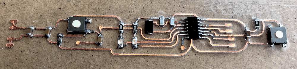
I decided to modify the echo hello-world board. I added two LED's, two Button's, multiple capacitors and resistors. The aim was to create a PCB that can be worn as a bracelet. To achieve this I had to make the board flexible, that's why I used a different technique to create it. The reason for this creation is that I want to make a flexible board for my final project.
Schematic Diagram
Schematic (also called circuit diagram) is a drawing that shows how the electronic components are connected. It acts like a map providing guidance on function, assembly and technical service. It's a language used by engineers to design and build a circuit.
Group Assignment
For this week's group assignment the scope was to test the equipment in our lab and to observe the operation of a microcontroller circuit board. Here you can find the documentaion.
Creating the Schematic
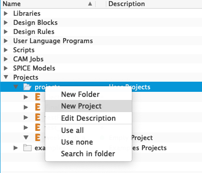
Before you start with the design you have to create a new project in Eagle. Just make a right click under Projects and select New Project.
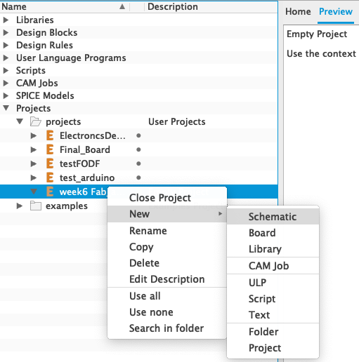
Then you need to create a new Schematic. Right click on the created project and select New --> Schematic.
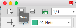
Save the file before you continue.
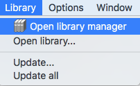
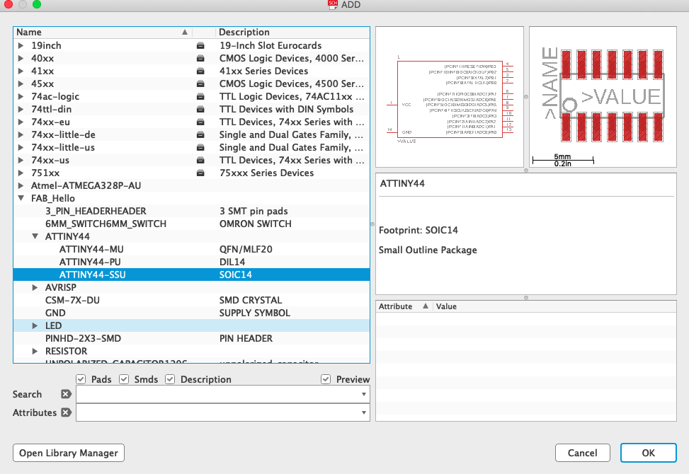
Eagle comes with a large library of components you can use in your design. But not all the components I needed for my design were incorporated, so you might have to add an extern library. You can do this by going to Library on the top menu and then open the Library Manager.
A new window will pop-up go to in use and then click on the Browse button.
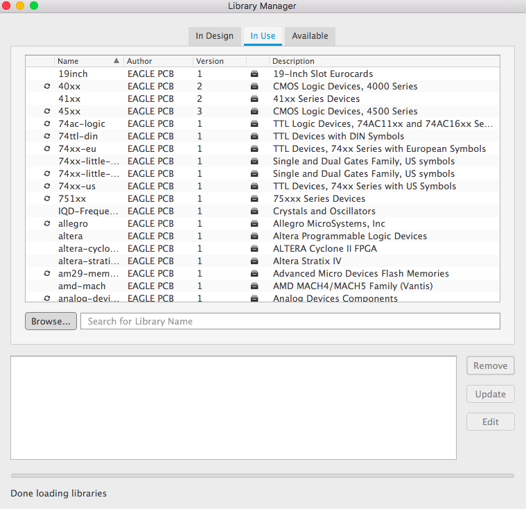
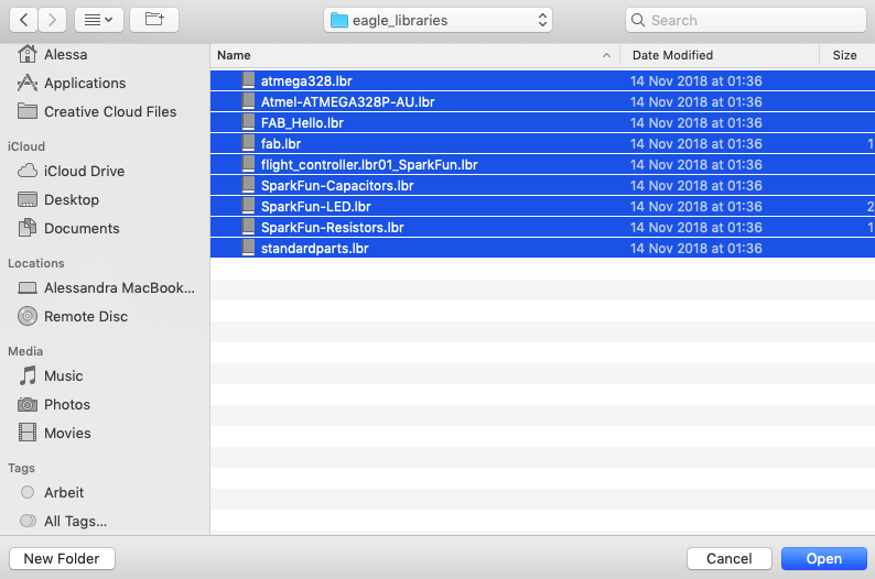
Now you can search for the library you want to import.
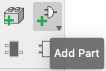
After importing the library you can add components to your schematic. Just click on the ADD Icon in the left toolbar.
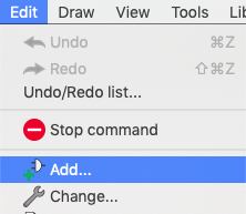
Or you can go to Edit in the navigation bar and click on Add...
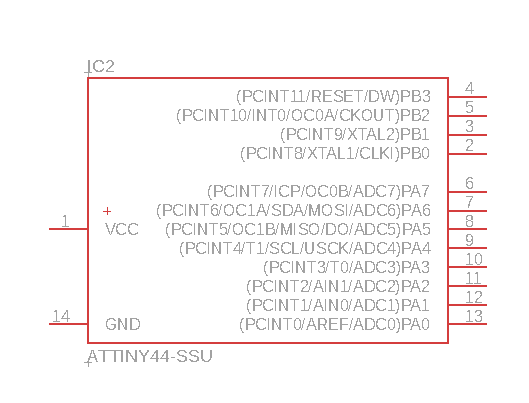
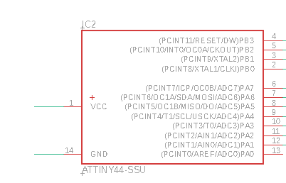
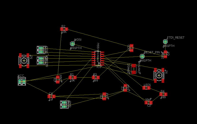
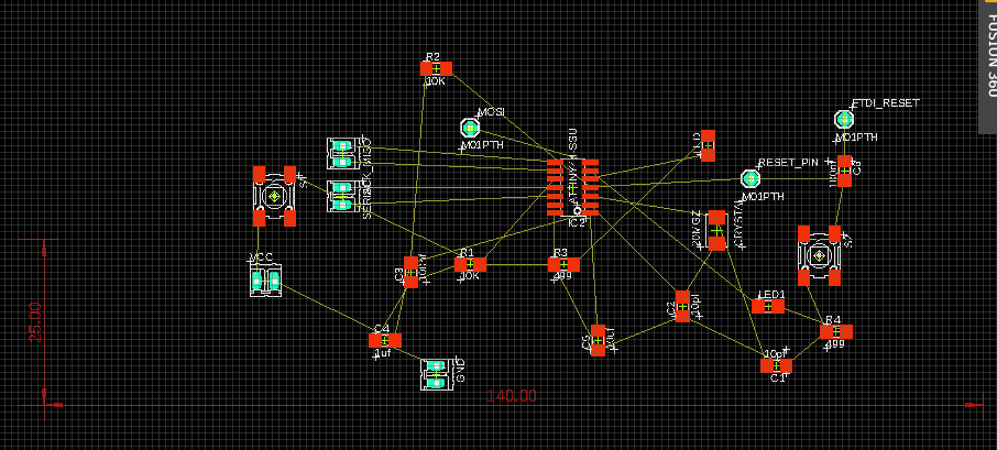
In the window that appears you can search for the components you need for your design. Below I added the ATtiny44. When you find the electronic component just confirm your selection and place it wherevery you like. Since I was adding the core of the board, I placed it in the middle.
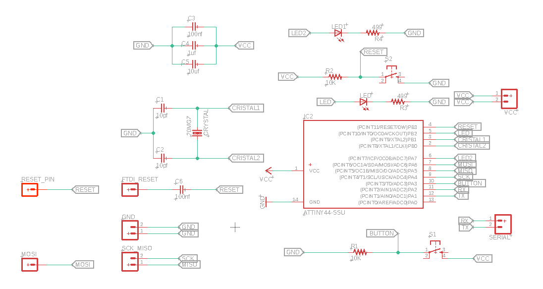
Now just repeat the steps until you have all the necessary components for your schematic. For my design I used the following components:
• 1 x ATTINY44: 2.7-5.5 volts Microcontroller
• 4 x M02 pin header. Two of them represent the multiple GND and VCC: used to provide power to the board. One for the MISO and SCK pins, since I had to split the ISP pins. And the last one for the TX, RX serial communication pins.
• 2 x LED 1206
• 4 x resistor 1206: two to regulate the voltage between the LEDs, one for the button and one for the RESET.
• 2 x 6mm omron switch. One as reset button.
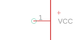
• 1 x VCC: Supply voltage
• 1 x GND: Ground
• 3 x M01 pin header: used for FTDI interfacing (reset pin), one for the other RESET pin and one for the MOSI pin.
• 6 x unpolarized capacitor 1206 that have differnt values (1uF, 10uF, 2 x 100nF and 2x 10pf): used to filter the input voltage (at different frequencies) so that the Microcontroller receives a stable power supply.
• 1 x 20Mhz Crystal: used to generate clock pulses required for the synchronization of all the internal operations of the microcontroller.
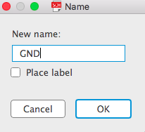
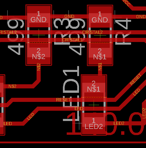
It is very important that you give your components a name, otherwise you might get confused. Click on the component and choose Name to change the heading.
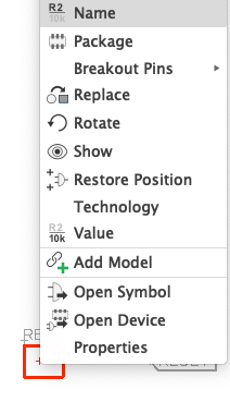
Some components as the resistor have a specific value, which you also need to declare. Just click on the component and choose Value to state the propper value for each resistor, capasitor and crystal.
After placing the microcontroller I started to draw the connections. To do this select the Net tool in the toolbar.

Then you select the end of the component. As soon as you see a green circle certify the selection.
Always label your connections, therefore you don't need to draw an endless line to the next component. Moreover it will give you a better overview of the schematic, because everything is held clearly and simple. You can find the Label tool near the net tool.
To change the outline of the label just select the design you desire in the control bar.
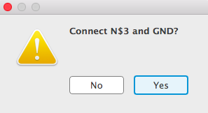
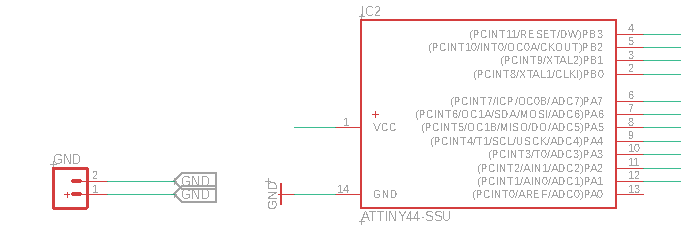
As soon as you select the label tool a new window appears. The name that you set in here, will be the component with wich you want to connect it. I wanted to connect the GND pin header with the GND output on the microcontroller.
If after confirming your selection this window doesn't pop-up, there is a high risk that your connection went wrong.
This is how it's eventually going to look like.
Just repeat these steps until you added and connected all the components. Below you see the finished schematic.
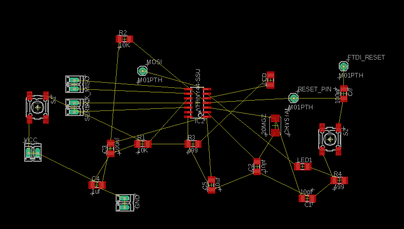
The Board Layout
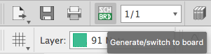
Once the schematic is completed, you can generate the board layout. To do this click on the Generate/Switch to board button in the top menu. This converts the schematic into a physical board layout. Furthermore make sure that the new board layout file shows all the components you created in your schematic.
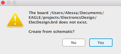
When this window appears confirm with YES.
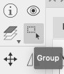
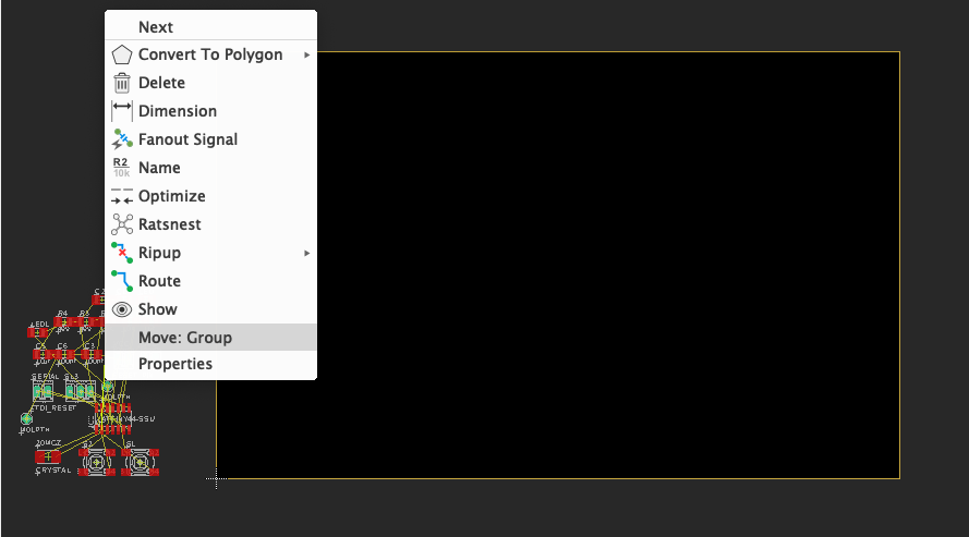
In the board layout window your design will be placed outside the canvas. To move the design you first need to select the entire design by clicking on the group element in the toolbar.
Now drag it into the canvas using the move element, which you can find nearby the group element.

Before you start routing you need to adjust the position of the components. They need to be placed in a way that they have as less crossovers between the connections as possible. Moreover it's also very important that you check, if you have a closed circuit. Otherwise you might need to modify the schematic.
Next use the rastnets tool to decrease the amount of connections. Since you moved the components there might be a different kind of strategy to connect them properly. So this tool basically just gets rid of unnecessary connections.

The idea was to create a flexible PCB that could be worn as a bracelet. To create this I measured my wrist to get the maximum length for the board. The maximum to go with was a 2,5 cm width with a 14 cm length.
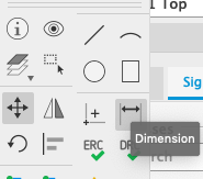
To stick to this size I used the dimension tool which you can find in the tool bar.
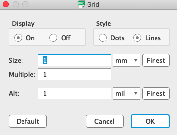
To make sure that the dimension lines are straight, I displayed the grid. You can find the grid configurations in the top left corner.

I set the size to 1mm and changed it later to 5mm.
With these dimensions I could easily move the components to create a nice board layout for the braclete.
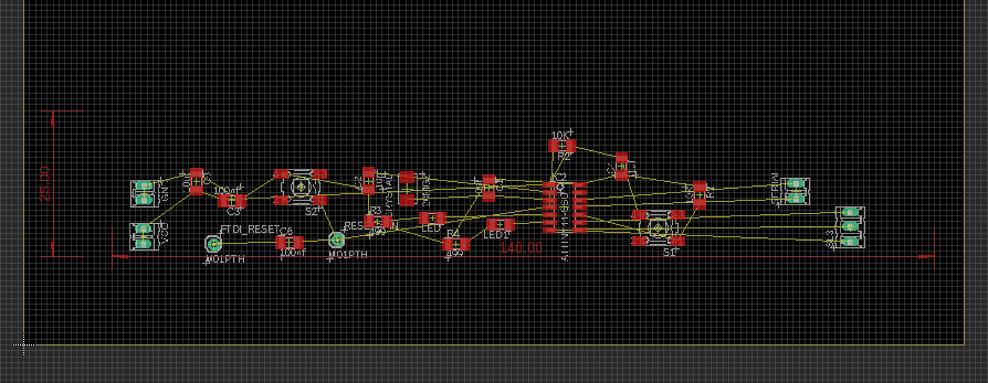
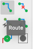
After you place everything in the propper position you can start routing. You can find the rout tool in the toolbar.
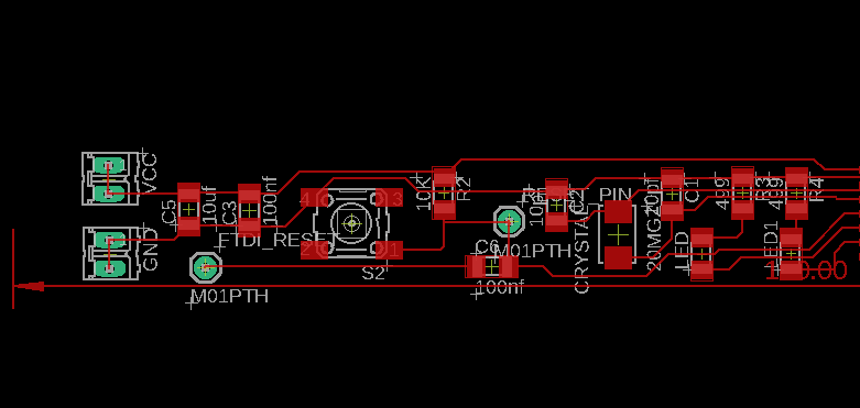
As I finished I recognized that the width of the routing was way to thin. Thin traces break very quickly, be it because of the heat during soldering or while milling the board. So it was matter of concern to change that.
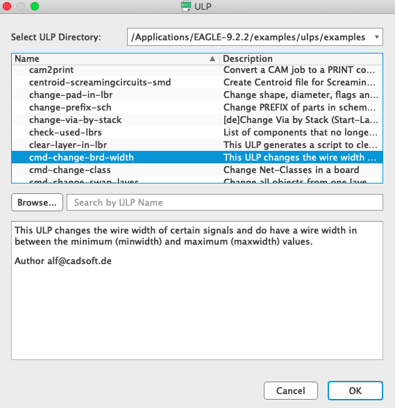
To to this I had to open the Run ULP window by going to File --> Run ULP.
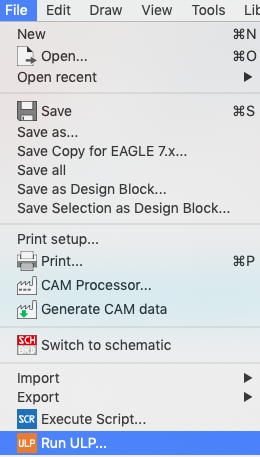
In the ULP window you can find the command change-brd-width.
In the following window you need to select all the traces by clicking on the Add all -->> button. Then set a new trace width in the input field. I decided to put the wire width to 12 to get a good end result.
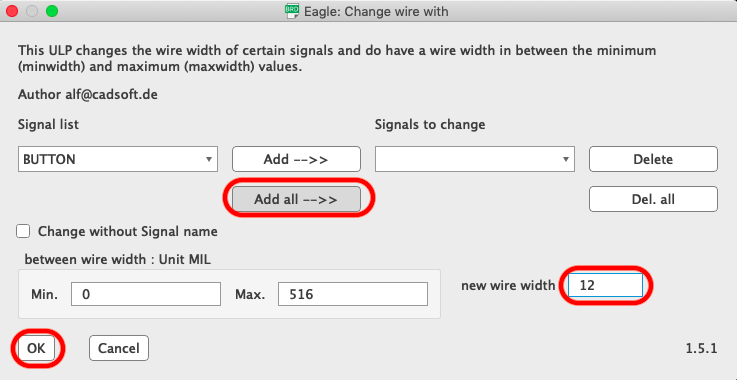
After enlarging the width of the lines, many connections didn't work anymore. Now there is too little space to lead two lines underneath a component. So I had to start all over again. I can only advise you to set the correct width beforehand.
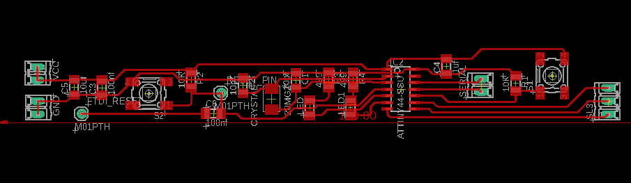
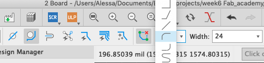
Furthermore I also changed the curves of the traces. Angular lines are far too difficult to cut for the machine, so I rounded them. In the control bar you can change the appearance of the traces.
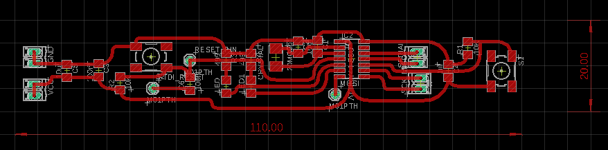
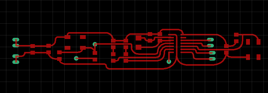
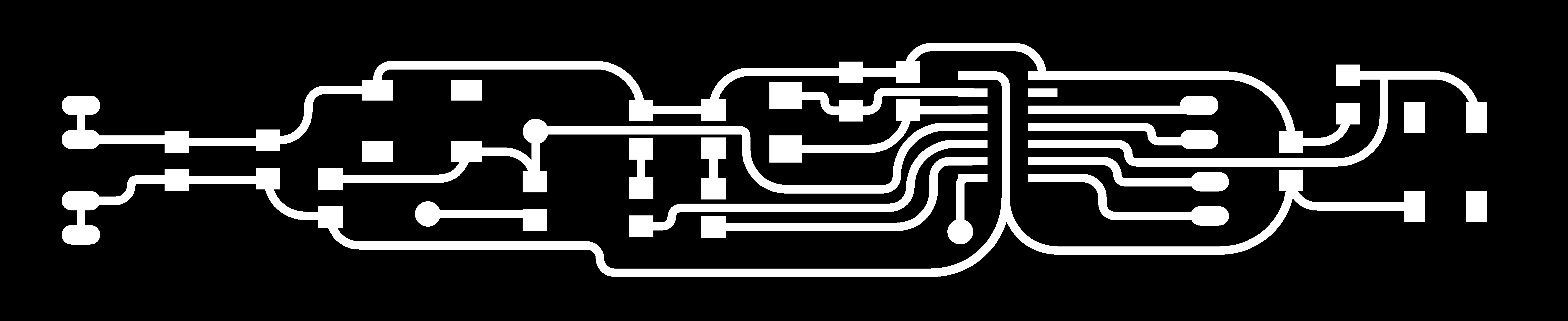
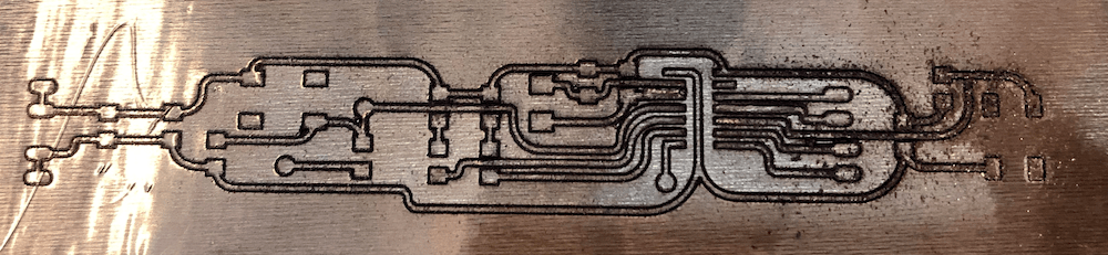
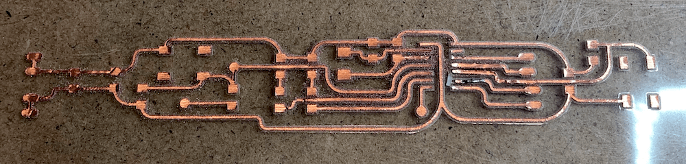
This is how the final board layout looks.
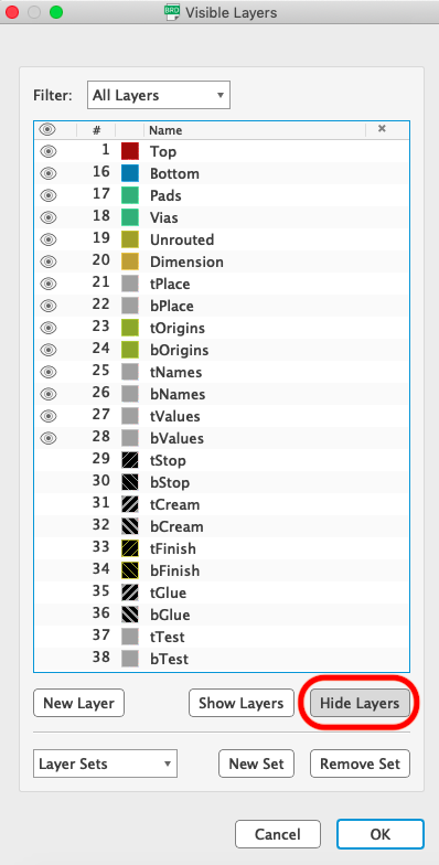
Next, you have to prepare the file for the machine. To do this you have to export the board as an PNG file. Remove all unnecessary details by going to View --> Layer settings....
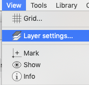
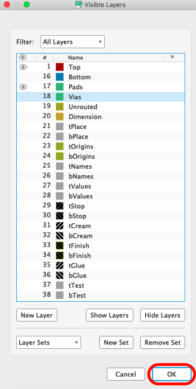
A new window will appear. Here you have to hide all the layers and then just select the essential ones the Top and the Pads.
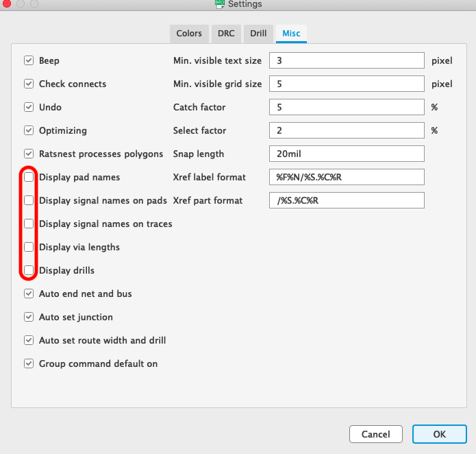
Then go to setting and deselect all the boxes below. If you are going to mill a board you usually display also the drills. But since I am using a copper sheet to mill the traces, I don't want to drill the holes for the through hole components. The copper sheet is about 0.2mm thick and not strong enough for such a construction.
Underneath you can see how it suppose to look like.
Finally eyport the file as an image.
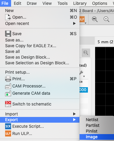
Furthermore the resolution has to be 1500 dpi, the area window and you also need to check the monochrome box. Then name the file and export it as PNG.
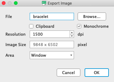
This is the final file, with it you generate the G-Code. In addition we don't need to create an outline, since we want to cut out the traces.
Preparing the G-Code
To prepare the G-Code I used the Fab Modules software, as I did in the Electronics Production week. There you can read more about how to use the software.
After importing the image, I selected the propper machine. The x, y and z axis values are set to 0, since the zero point/start point of the machine is set manually.
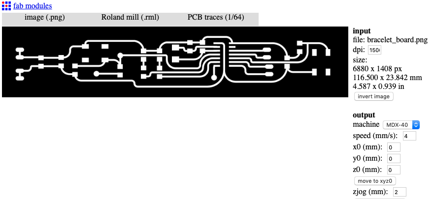
The idea was to stick the copper sheet on a flexible plastic film and then mill the tarces on the copper with the Roland. So for this particular job I used a cut depth of 0.0mm, to prevent the bit from cutting too deep into the copper sheet and cut through the plastic film. To get a very accurate result I used a 0.1mm tool. The offset is set to 1, since the aim is to only expose the traces and remove all the unnecessary copper from the plastic film.
Using the Roland Mill
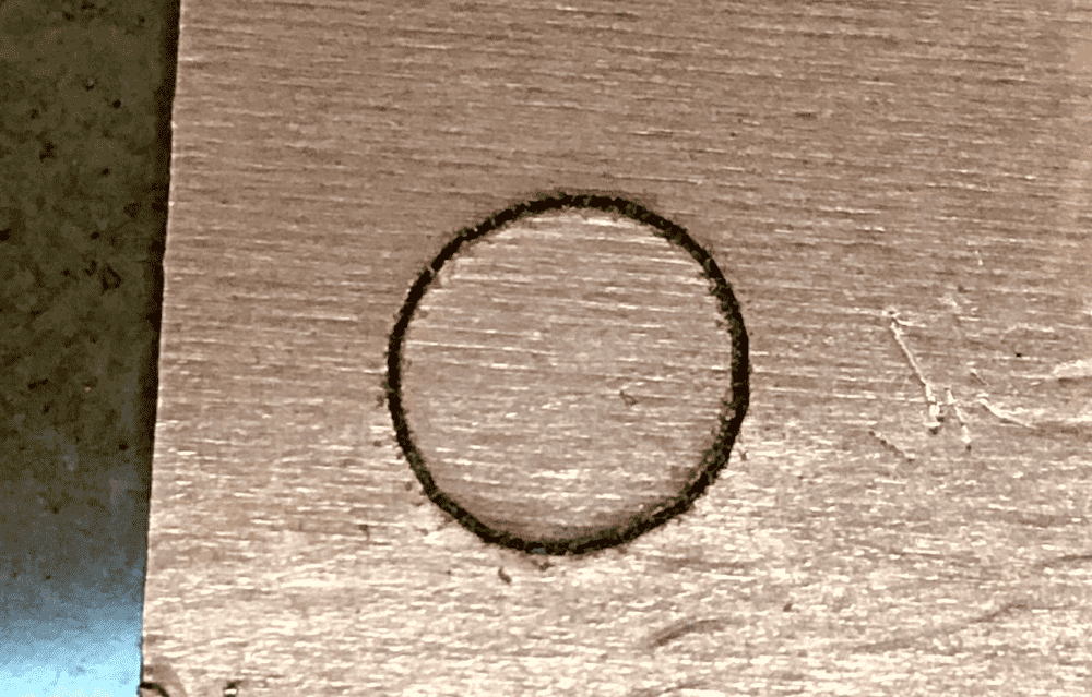
Before I started to mill the board, I had to test the idea, since no one has used this technique before. I decided to use this technique, because the CNC Machine very percise compared to the vinyl plotter. So I drew a circle using Gimp and then generated the G-Code with Fab Modules.
In the Electronics Production assignment you can read more about how to use the Roland Mill.
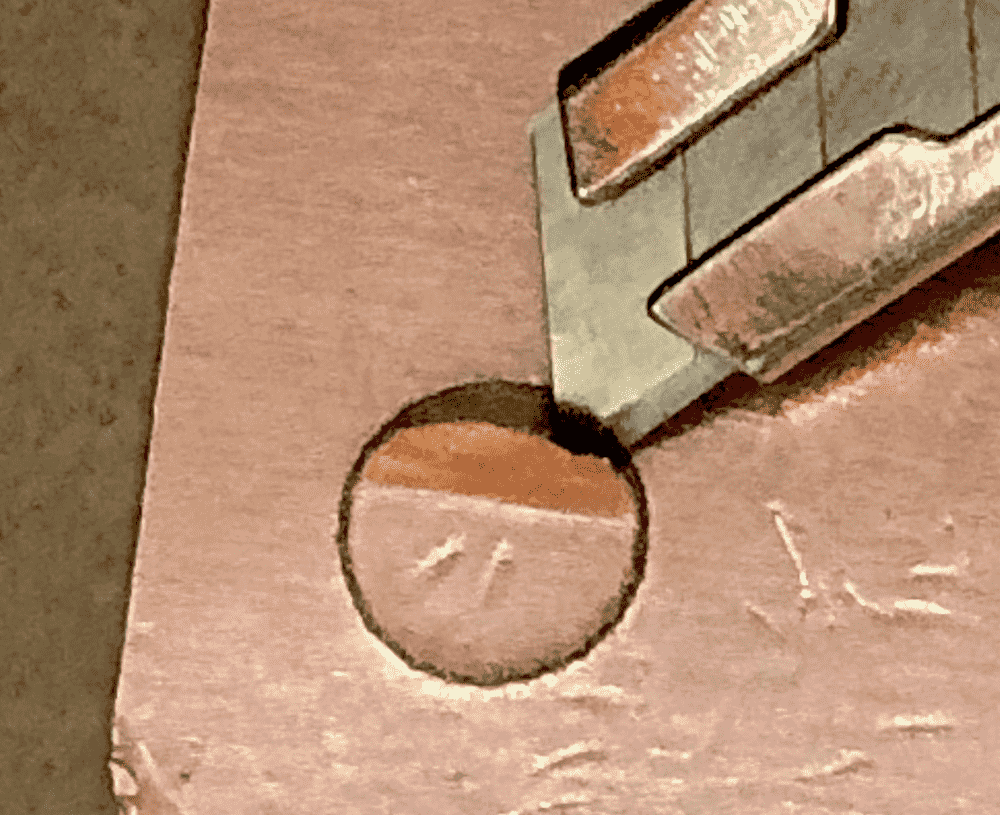
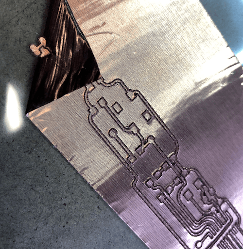
To secure the plastic film with the copper sheet on the bed of the machine, I used paper tape. The first test went really good.
It was also really easy to remove the sticky copper sheet from the plastic film.
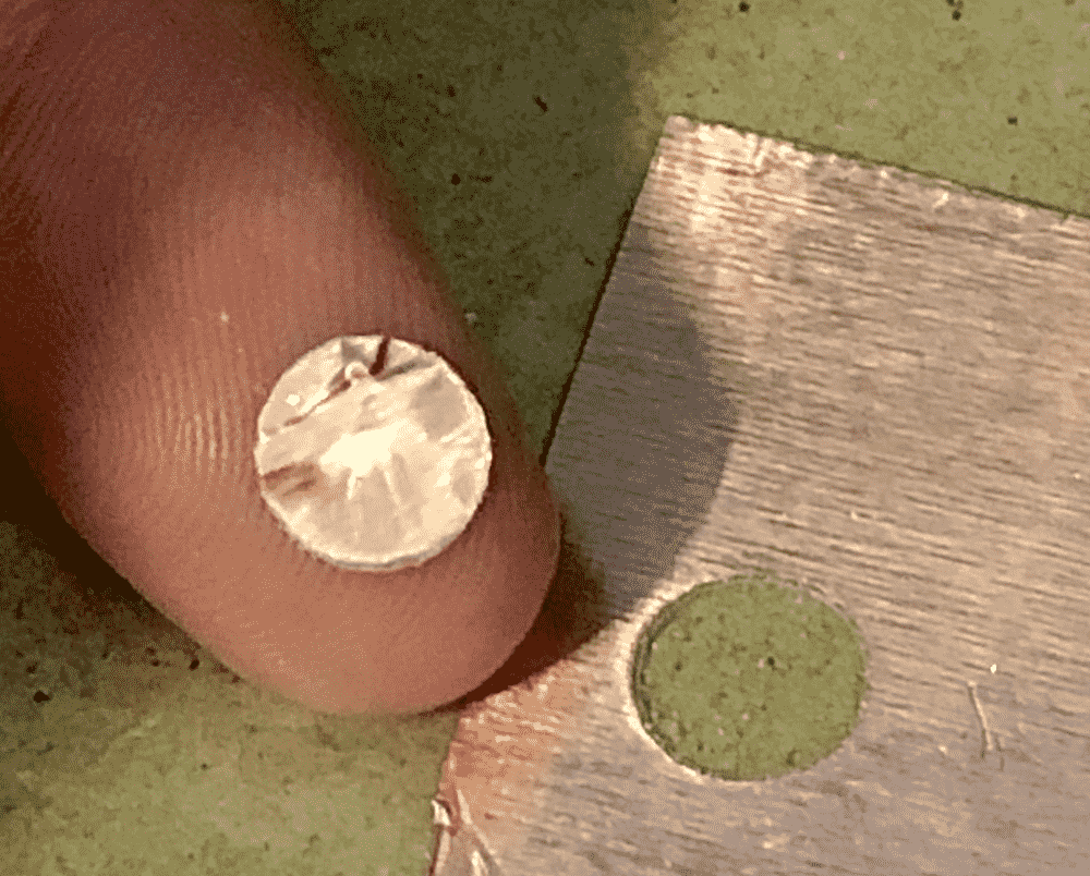
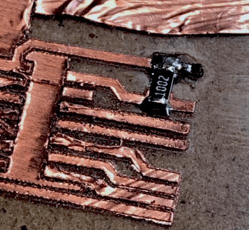
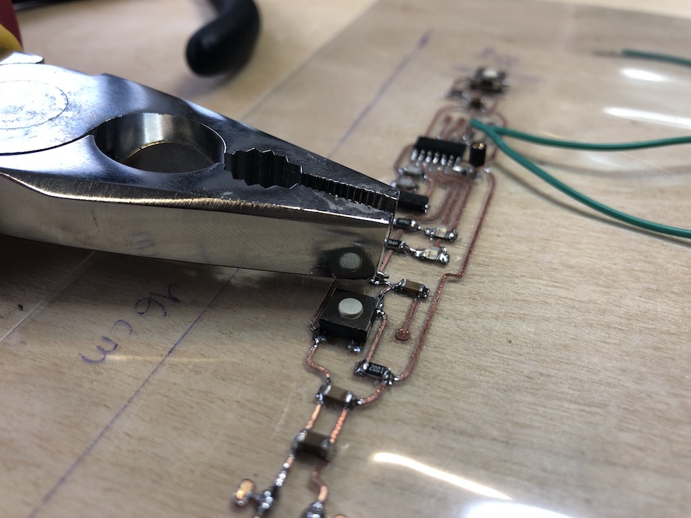
Since everything went as planed, I tried the mill the traces of the microcontroller. Underneath yoe have the result of the process. Here I recognized that the bit went a little to deep and I had also to reduce the speed, so that the bit won't tear the traces.
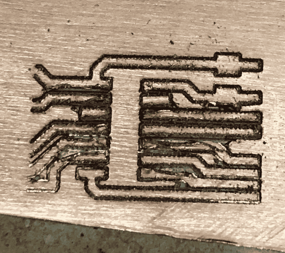
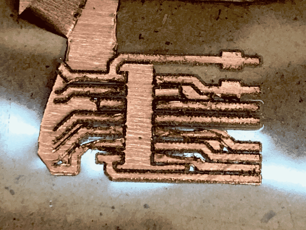
After a few more tests I finally figured out the right settings for this job.
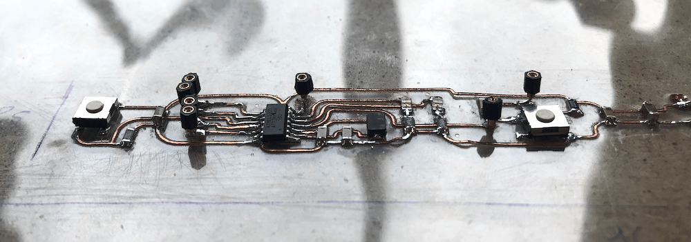
This is how the outcome looks like.
Soldering
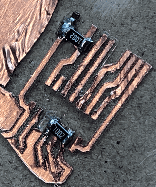
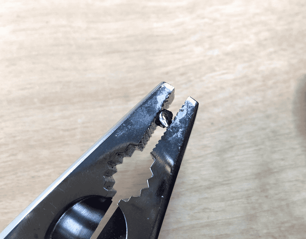
Before I started soldering I had to remove the copper arround the traces, which could be easily removed.
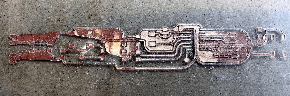
Then I first used a test piece to practice the propper soldering technique, as this part was very challenging. The goal was to solder everything quickly, without exposing to much heat to the plastic film. So that the soldering material adheres quickly, I used a flux pen.
Basically I used the same technique as I did in the Electronics Production week.
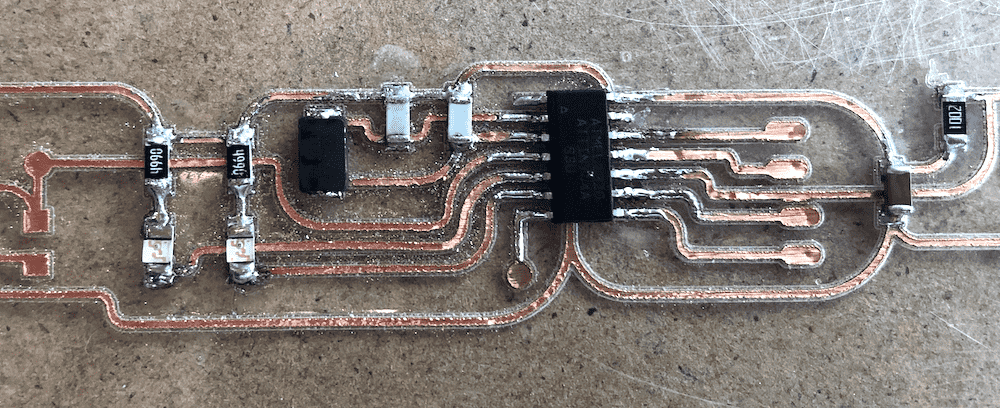
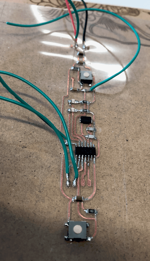
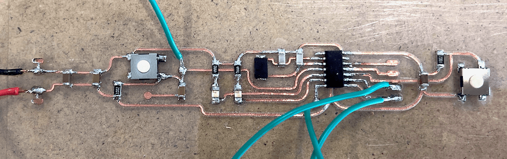
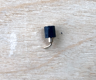
At last I soldered some wires on the VCC, GND and programming pads. This is only a temporary solution, because the idea is to use small pin headers.
Programming
To give the microcontroller functionality I used a Arduino Uno board as ISP, but you could also use something else (for example the FabISP). First the Arduino needs to act as programmer by uploading the ISP sketch.
Before connecting the PCB to the Arduino Uno, check all the connections with the multimeter, to be sure that you have a closed circuit and that you do not have any shorted circuit. If everything is well-connected, you can go ahead and connect the PCB with the Arduino.
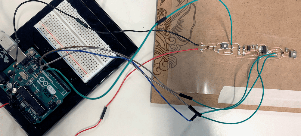
Then go to Tools and set the correct configurations of the board. Since I included an external 20 MHz cristal, you need to select it as clock, otherwise it will use the internal clock of the Attiny 44. As soon as everything is set burn the bootloader.

To show that the board works, I uploaded the Blink Example sketch.
Improvements