5. Electronics production
Week 05: Feeling a little nervous heading into this week. Finally an assignment week where I have zero context. Deep breath…and jump!
Individual Assignment: Make an “In-Circuit Programmer”
- 2 options to choose from…FabTiny (supposedly buggy…not much experience with this board in the Kamakura Node) & FabISP (Recommended)
- I prefer the aesthetic simplicity of FabTiny…so I will bravely/stupidly challenge the making of this PCB…
The FabTinyISP…Some Basic Understanding
- Also called the FabTinyStar
- A version of an AVR ISP…AVR is a microcontroller type, ISP stands for “In System Programming”
- AVR (Alf and Vegard’s RISC processor?) was developed by Atmel now owned by Microchip Technology…modified Harvard architecture (where program and data are stored in separate physical memory systems that appear in different address spaces…but having the ability to read data items from program memory using special instructions), 8-bit RISC single-chip microcontroller with on-chip flash memory for program storage (not one time programmable ROM, EPROM or EEPROM)…used by applications as embedded systems (popular with Arduino)
- The TinyAVR or the “ATtiny” has 0.5-32KB of program memory, 6-32pin package, limited peripheral set
- The Attiny can be programmed by a device called a AVRISP mkII
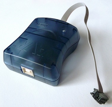
…connects to a PC via a USB.
A more detailed description of the ATtiny can be found in the Wiki here link to ATtiny Wikipage
- After programming, the FabTinyISP…has no reset switch (software command resettable), target power switch or PTC Thermistor…the Makefile has been replace, targets for programming the fuses has been added…designed solely to be an ISP programmer not a general purpose tiny45 board
Assignment Procedure:
Followed this tutorial tutorial to make the FabTinyISP Programmer.
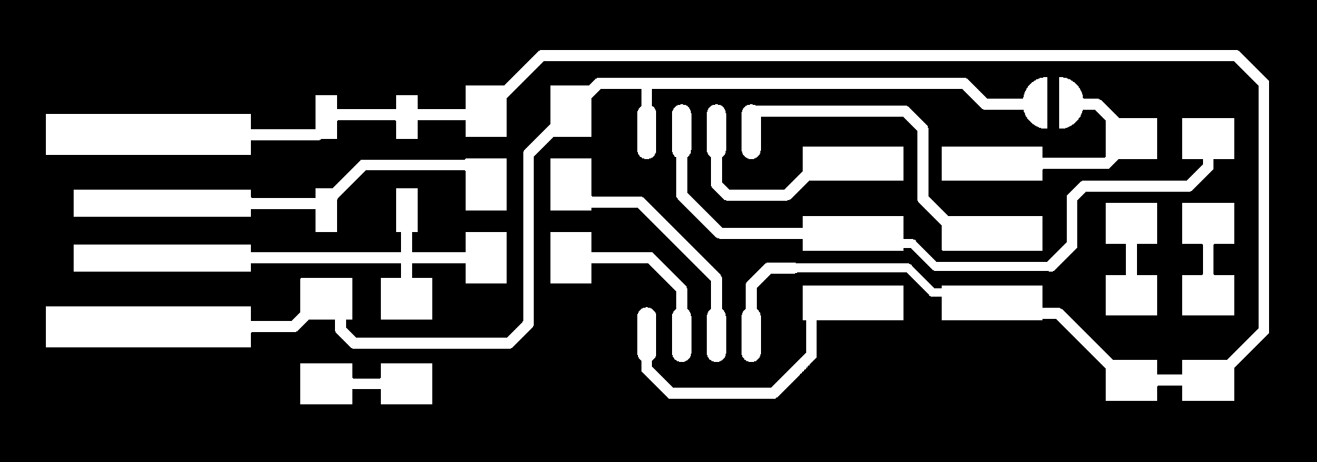
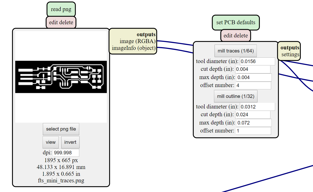
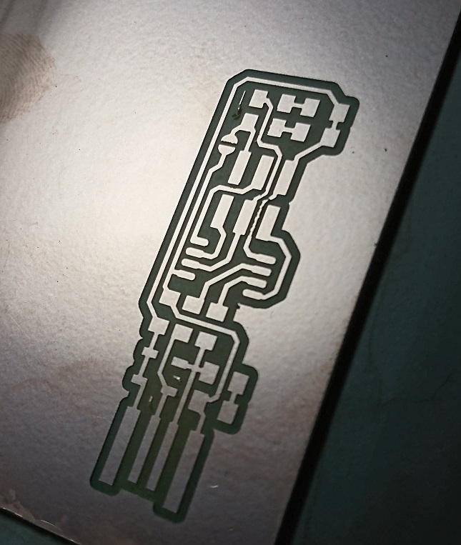
- Get FabTiny ‘Trace’ and ‘Outline’ image files (PNG format)
- Convert the Images to RML files for use by the milling machine…mill the PCB
- “Stuffing” (assembling electronics parts on the PCB board) with the prescribed components for the FabTiny
- Install various software onto local PC to upload programs onto the finished In-Circuit Programmer (ICP)…to make it into a programmer.
Followed this excellent (FabTiny Tutorial) by Brian Mayton and remixed/updated by Craig Hobern
- Noted in the tutorial that the FabTiny build will become an AVR programmer but will need a working AVR programmer in the process (a AVRISP mkII)
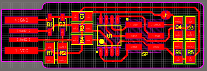
The method to fulfill steps 1 & 2 of the individual assignment procedure is identical to those utilized in the group assignment “Test PCB” milling, decribed here…link to Wk5 group assignment
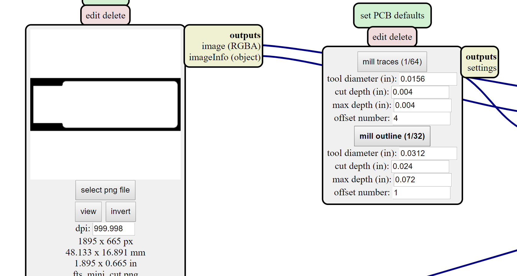
Step 1: Upload the PNG image files for the PCB’s “Traces” & “Outline”
-
Easy and straight forward procedure

-
Noted that the image files are 1000dpi resolution (what is the minimum useful resolution?)
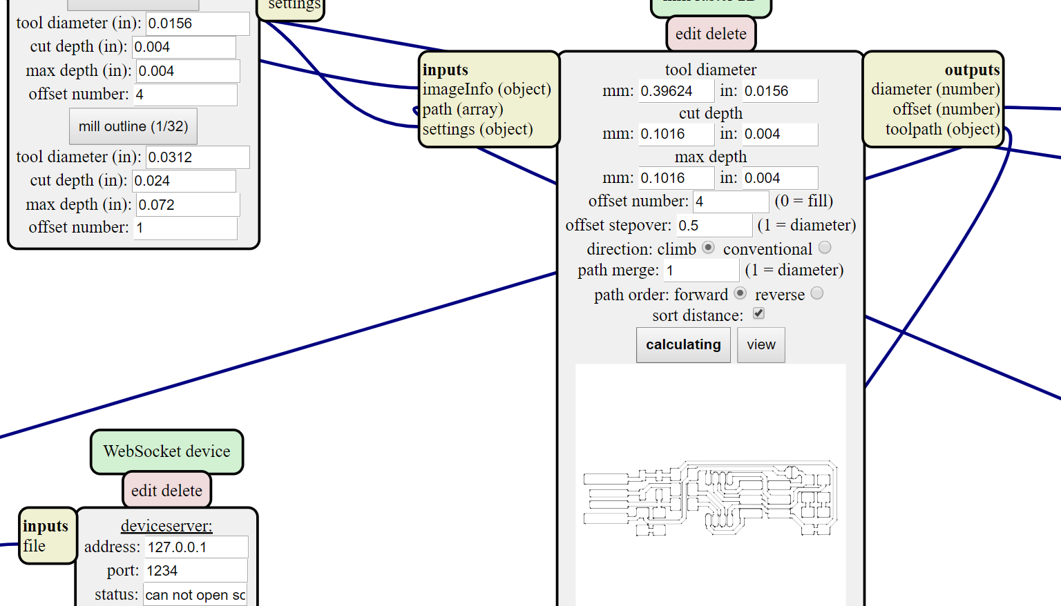
Step 2: Generate RML milling files from the PNG files using Mods
- Easy and straight forward procedure, following the procedures used to make the “Test PCB” for the group assignment
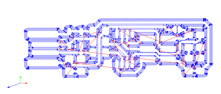
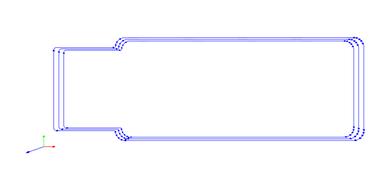
Step 3: Mill The FabTiny Circuit Board
- Everything went smoothly, following the procedures used to make the “Test PCB” for the group assignment
Step 4: Wash, Deburr and Scuff the PCB surface
- Soap and water for washing (…to remove oils, make solder stick better?)
- Deburr the edges of the PCB by scraping with a craft knife
- Scuff the PCB surface with some steel wool (to =make solder stick better?)
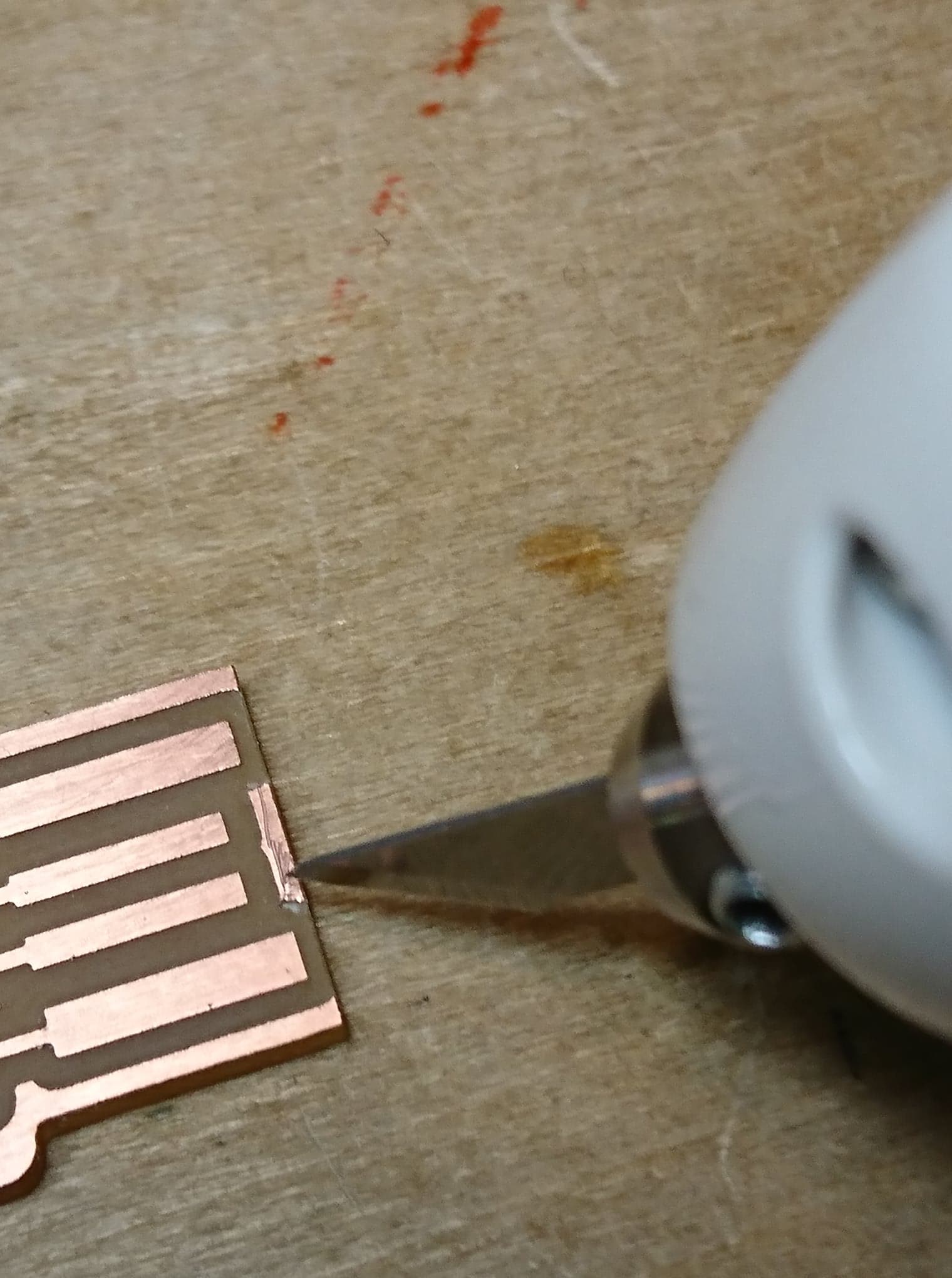
Step 5: Remove Excess Copper
- Removed excess copper with an ultrasonic knife…definitely overkill but it was an interesting first experience with this tool
Step 6: Flux the PCB Surface
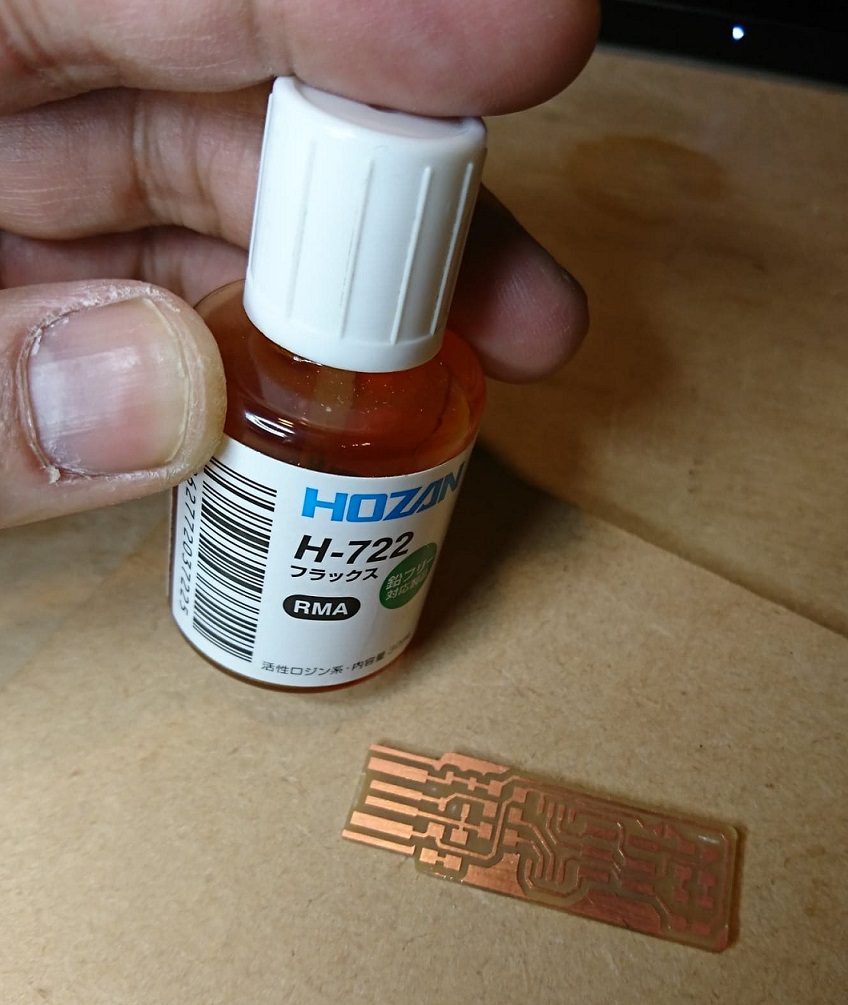
- Preps the PCB surface for soldering on components
- Just brushed the flux over the surface and let it dry (flux makes for better solder joints)
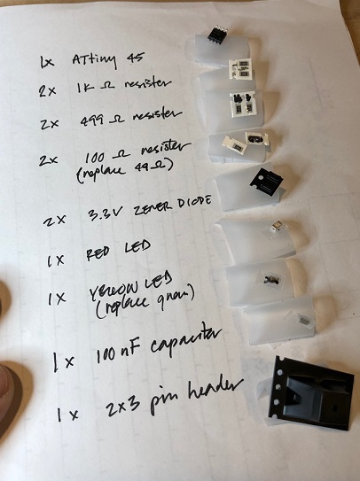
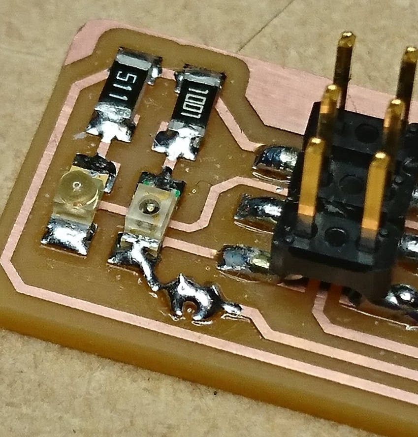
Step 7: Grab Components
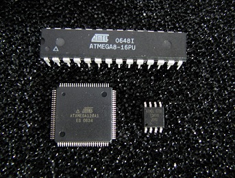
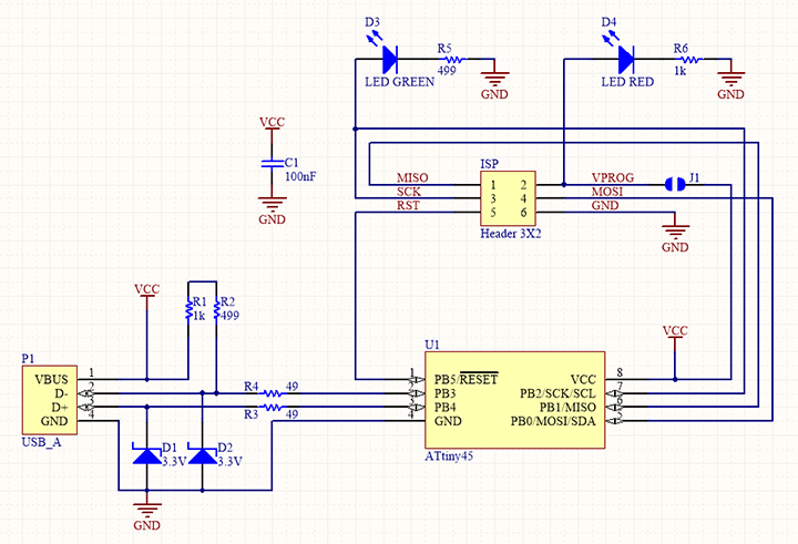
The FabTiny Components:
- 1x ATtiny45 or ATtiny85
- 2x 1kΩ resistors
- 2x 499Ω resistors
- 2x 49Ω resistors
- 2x 3.3v zener diodes
- 1x red LED
- 1x green LED
- 1x 100nF capacitor
- 1x 2x3 pin header
- Following my classmates, I taped all the components individually next to their names written on a piece of paper…this helped to keep the very tiny pieces organized and save time having to figure them out from a pile
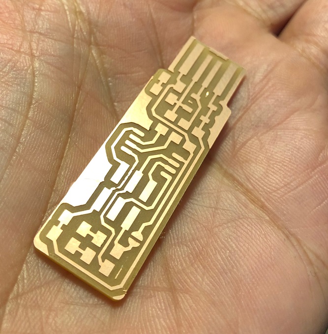
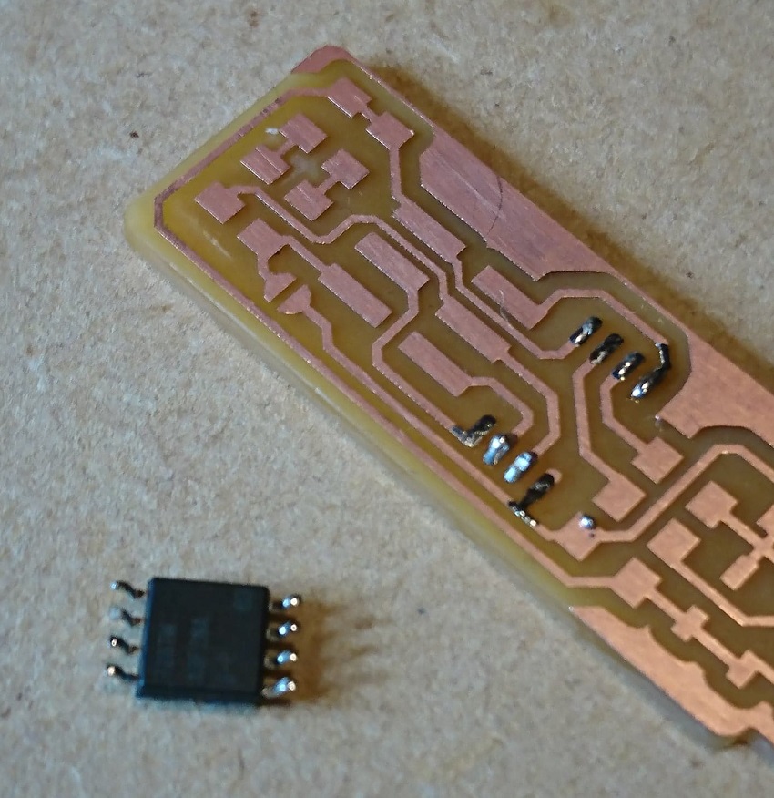
Step 8: “Stuffing” the Components
- “Stuffing” mantra…inside to outside, low to high…I soldered the ATtiny45 chip First, working down my list…noting components that be oriented a specific way (the ATtiny, LEDs, Diodes)
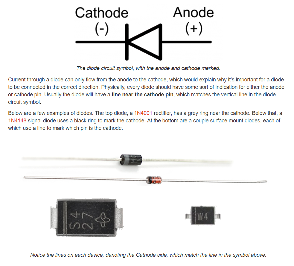
Note: we should have a book of printed out data sheets for components where orientation of cathode and anodes matters
- Mistake 1: Absentmindedly, I soldered the ATtiny chip on in the wrong orientation (the dot in the wrong location relative to the board as specified by the diagram)
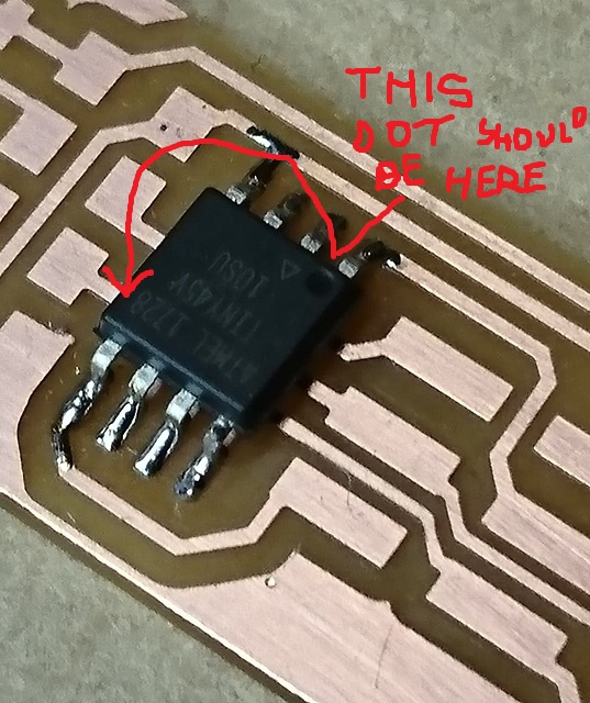
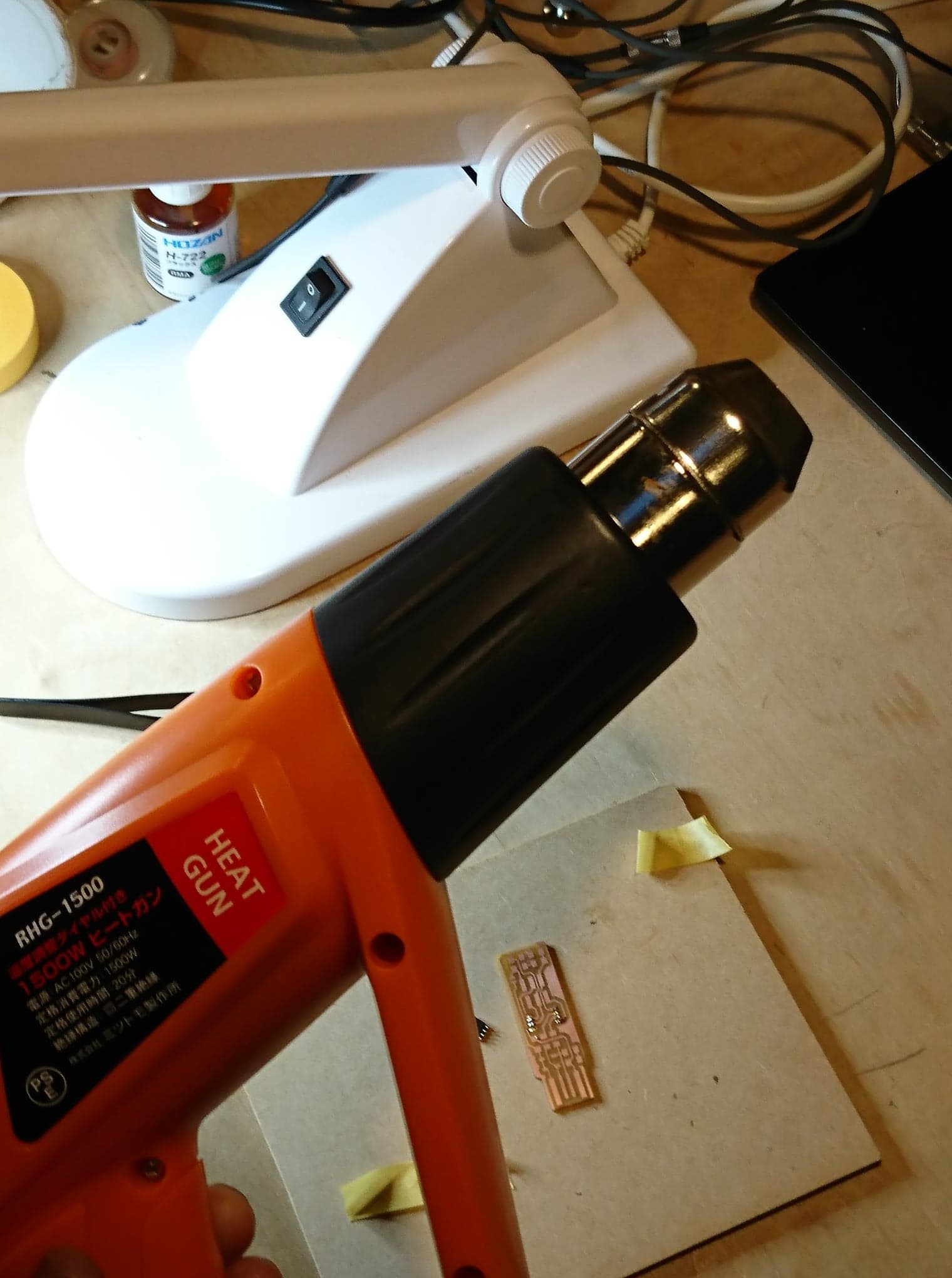
- Got to try out the technique Niel mentioned in the last lecture…use a heatgun to desolder…works great!!!Took only a few seconds
- Mistake 2: Also soldered the diodes on wrong…cathode does NOT point towards ground for this component (like LEDs) like I assumed…desoldered/resoldered into the correct orientation
- All other components soldered on without issue
- In addition to the components, the tutorial instructs to solder the VCC to VPROG pin and create a connectivity bridge
- Used a multimeter to check all solder joints for conductivity…all joints generated good tone sounds
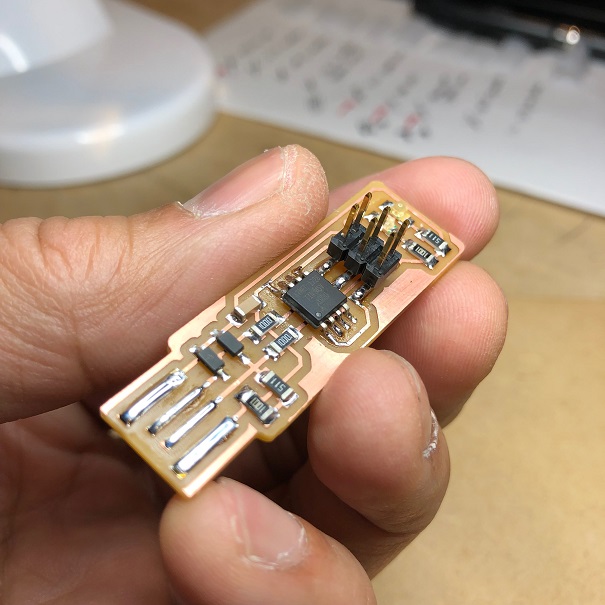
- Super glued a layer of plastic to the bottom of the FabTinyISP to make it a little thicker and hopefully seat better into USB slots
Step 9: Installing Software & Drivers
Followed required Windows software installation tutorial for this step here
Installed AVR Toolchain
AVR Toolchain is…a collection of tools/libraries used to create applications for AVR microcontroller. Includes complilers, assemblers, and standard C & math libraries. The files to install the AVR Toolchain can be found here
Installed GNU Make
- This freeware…is a tool which controls the generation of executables…of a program from the program’s source files.
- GNU Make gets its knowledge of how to build your programs froma a file called Makefile, which lists each of the non-source files and how to compute it from other files.
- A Makefile should be written for every program written…to make it possible to use the Makefile to build and install the program
- A rule in the Makefile tells GNU Make how to execute a series of commands in order to build a target file from the source file
- There are specific conventions to write Makefiles
- More about GNU Make here link
Installed AVRdude
- This program is an AVR uploader/Uploader utility to manipulate the ROM and EEPROM contents of AVR microcontrollers using ISP techniques
- Command line interface operated
-
Paths to each of the software executable files added in ‘Environmental Variables>Paths’ line with tutorial instructions
Zadigs software installed to enable installation of the FabTinyISP’s Window’s Driver
- Zadig could not “see” the FabTinyISP even after its insertion into the PC…problem
Mad Hatter sensei to the rescue again…connected to the AVRISP_mkII and then connected to the PC…Zadig was able to install the driver “Libusb-win32” (It is IMPORTANT that this specific driver, not another USB driver is installed…or else the ISP will not be recognized properly by Device Manager)
Step 10: Programming the FabTinyISP
- Uploaded the firmware source code here link…then extracted the zip file
-
In the CLI and changed directory to root(?)…ran “Make” program…builds a hex file to program into the FabTinyISP
-
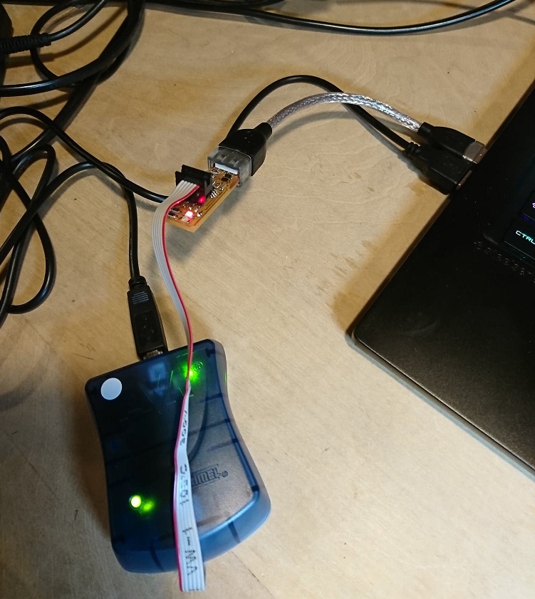
Will need the AVRISP_mkII to program the FabTinyISP
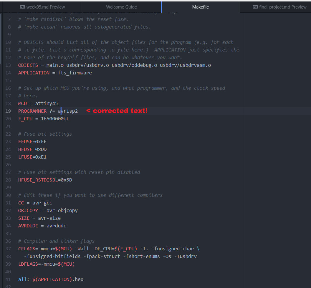
- To let the PC see the AVRISP_mkII Edited the Makefile as per tutorial instructions using Atom but mistyped the edit…typed “rvrisp2” to identify as the value for line “Programmer ?” instead of “avrisp2” (to identify the AVRISP_mkII).
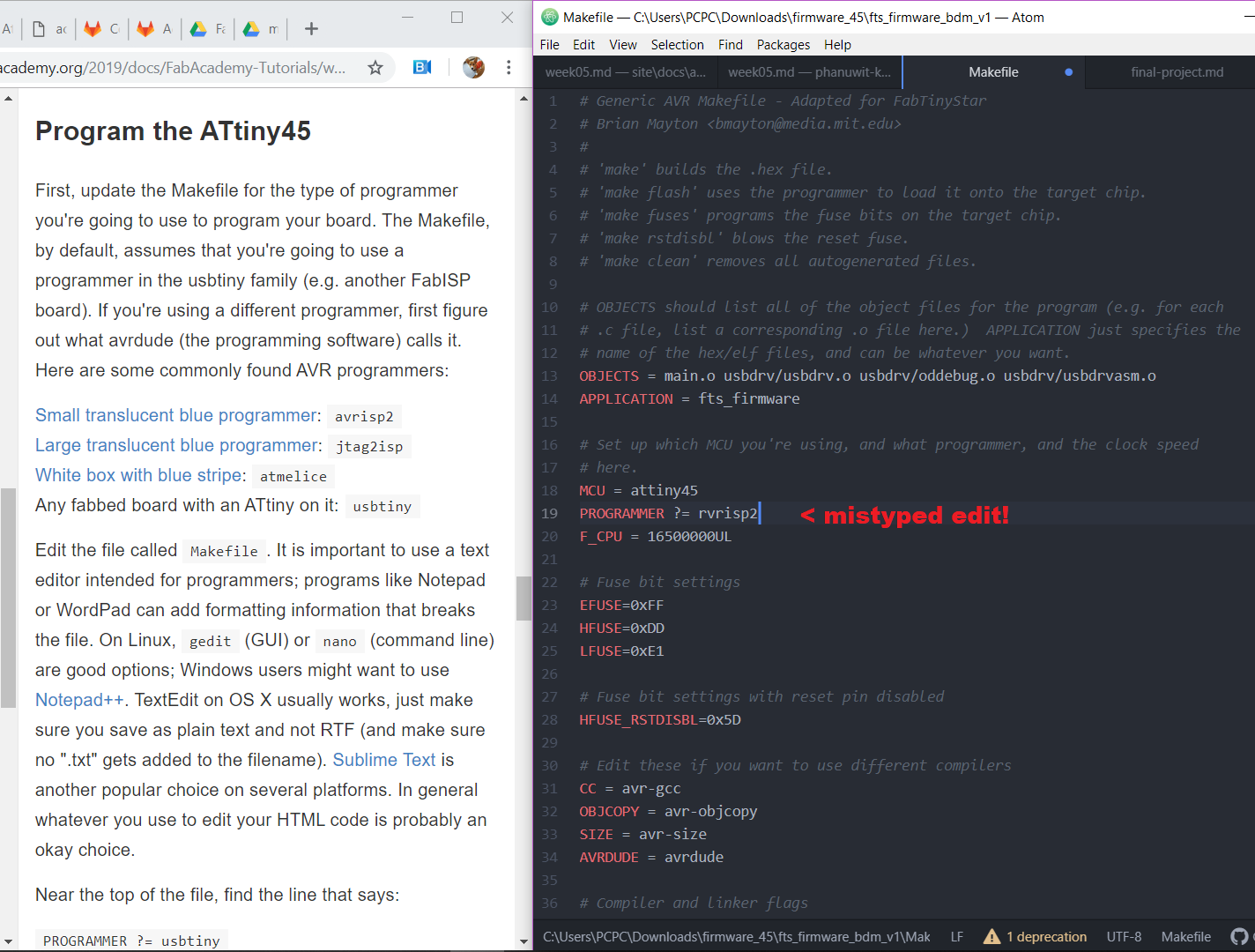
- This caused a debugging session that lasted over an hour…
- Checked the board itself for circuit issues…all OK
- Checked that Pin 1 on the connector is connected to Pin 1 on the FabTinyISP board…OK
- Checked that the ATtiny45 is now correctly oriented…OK
-
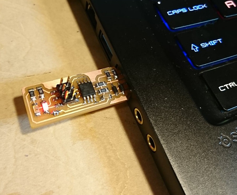
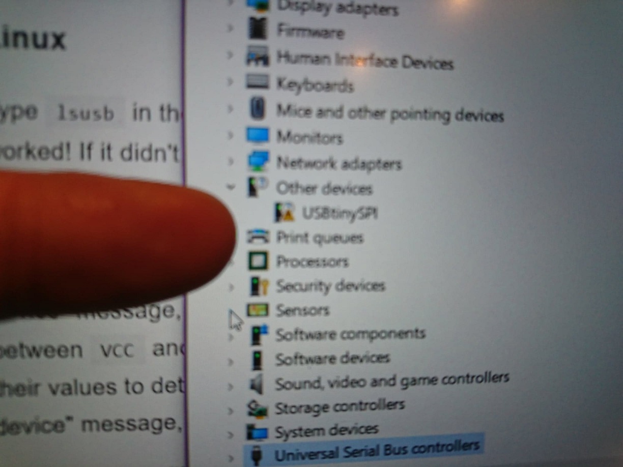
Checked the built up solder USB connector pads and connection to the PC is good…all OK (red LED turn on, PC does not reject the device but it doesn’t show up in the Windows Device Manager)
-
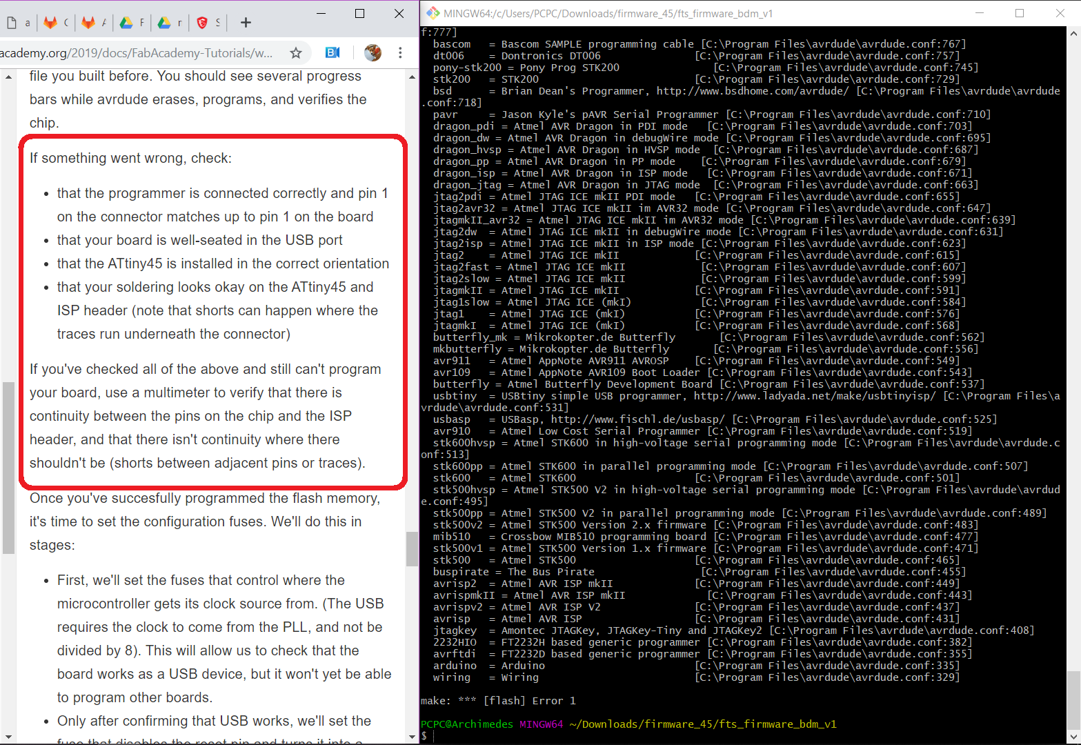
Attempts to flash the FabTinyISP fails
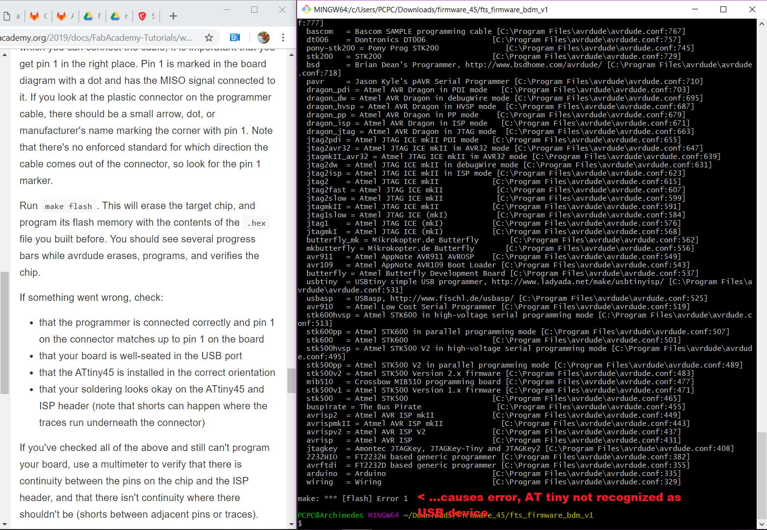
- When the FabTinyISP is plugged into the PC…it is not recognized by Windows’ Device Manager
- When the FabTinyISP is connected to the AVRISP_mkII and both plugged into the PC…the PC generates an error message…”doesn’t recognize the device”
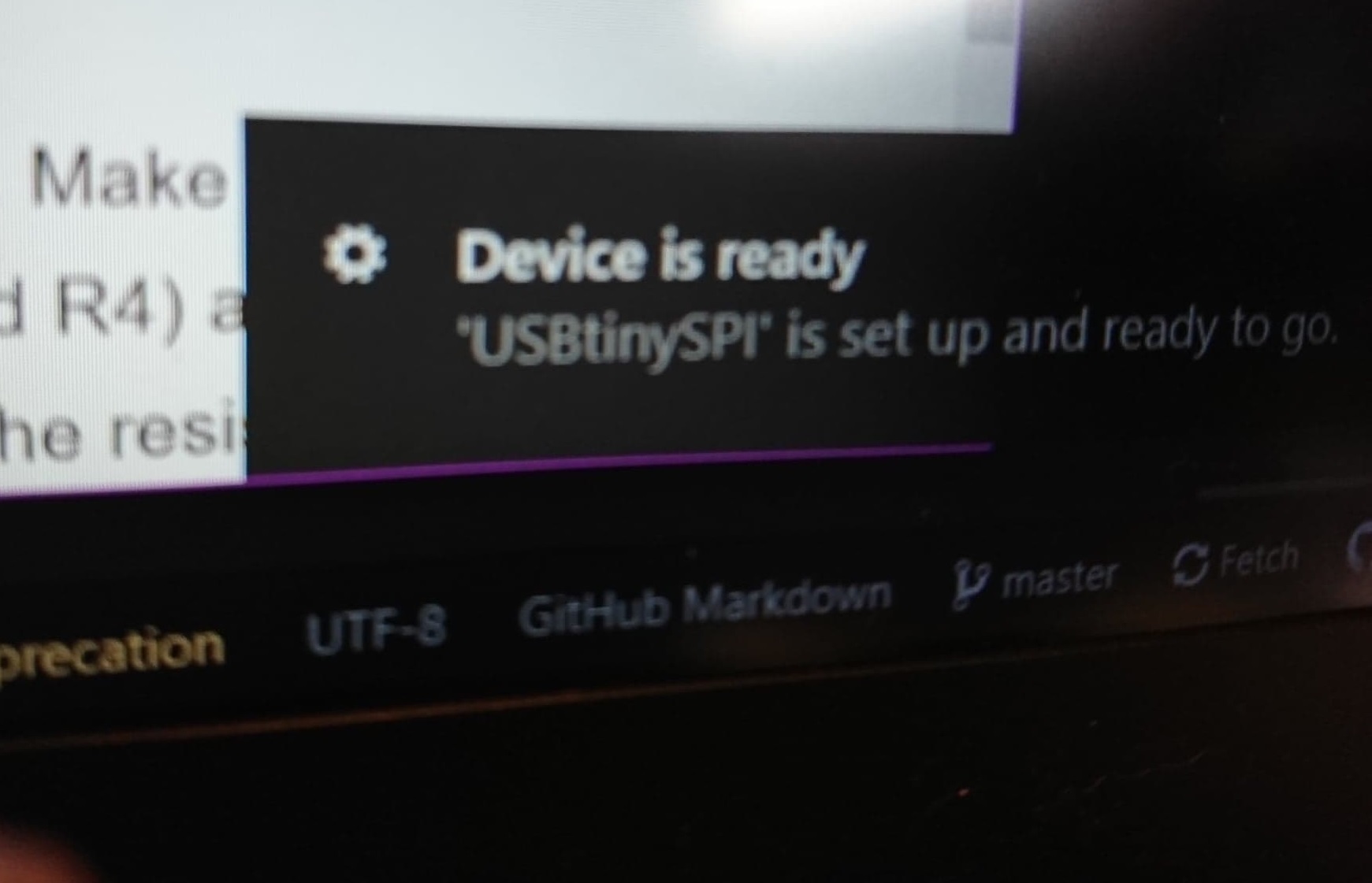
Thankfully one of the instructors (arigatoh Mad Hatter sensei!) who was helping with debugging noticed the typing error…made the adjustment and…success!! The mistyped instruction caused the PC not to recognize the AVRISP_mkII which had caused the error
- Ran “make flash” in the CLI to erase the target chip and replace its flash memory with the hex file generated by the “make” command earlier
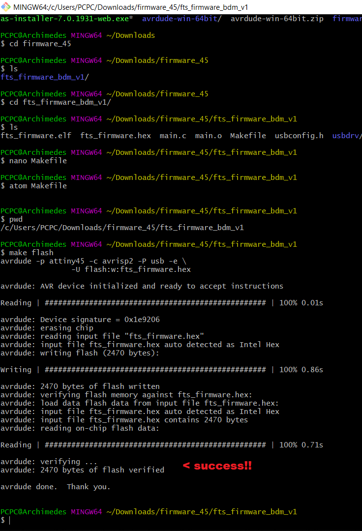
…flash successful, time to “set the configuration fuses”
-
Set the fuses that controls where the microcontroller gets its clock source from (from PLL not divided by 8)…allow the FabTinyISP to be recognized as a USB device…success!!!
-
Disable reset pin, turning it into a regular GPIO pin…allowing the FabTinyISP to use this pin to program other boards…but disable its ability to be programmed again itself…frome the CLI ran the “make fuses” command
-
Blowing the FabTinyISP’s fuse…disconnect from the AVRISP_mkII, plug the FabTinyISP directly into the PC using the USB port…from the CLI ran the “make rstdisbl” command…this done, AVRdude can no longer talk to this FabTinyISP via its ISP header again.
-
Last step…desolder the VCC to VPROG pin solder bridge made earlier…this done, the FabTinyISP is now a programmer
Done!!! Not sure I understood everything that happened in the last part of the session…but done for now.
Appendix - Misc Research
Brian’s FabTinyISP Version
“This version (the “FabTinyISP Minimal” is a minor revision to Zaerc’s version 0.3 (Bas), with small modifications:
The reset switch and target power switch have been removed. The reset switch adds cost and isn’t incredibly useful on an ISP programmer, as the target can be easily reset through a software command. The target power swtich has been removed as providing power to the target through the programming port is usually discouraged. Users who understand the implications of this are welcome to build one of the FTS designs with the switch. The copper ground pour has been removed and replaced with individual ground traces; this allows novice solderers to mill away more of the copper. All components solder to clearly defined pads on both sides. The extra pads connecting to the USB data lines were removed; this version is targeted solely at being an ISP programmer rather than being a general-purpose tiny45 board. The PTC thermistor was removed; as this part currently isn’t in the inventory most users would build it with a 0Ω resistor anyway. As the option to provide target power has been removed, it should be much more difficult to create a condition where the polyfuse would be needed. The Makefile has been replaced. Targets for programming the fuses on an ATtiny45 have been added. The original Makefile also results in problems on case-insensitive filesystems (i.e. Windows).”
Using FabTinyISP on Modern USB
“The FabTinyISP is a “low-speed” USB 1.1 device. This is the slowest (and one of the oldest) of the USB device types. Typically used for mice and keyboards, low-speed devices operate at 1.5MHz and have much less strict timing requirements, which enables a purely software-based implementation of the USB protocol to be used (the ATtiny45 does not have hardware USB capability).
While all later USB versions should be backwards-compatible with older devices like the FabTinyISP, there are a few things to keep in mind to avoid issues:
Avoid using USB 3 hubs. These don’t always work well with low-speed devices and may affect the timing of signals that the FabTinyISP depends on. USB 2 hubs seem to work okay in most cases. If you need to adapt from USB-C, it is best to use a cable-type adapter. This puts a lot less strain on the ports (on your laptop, the adapter itself, and the programmer) as compared to a plug-style adapter with no cable.
Beware of USB-C adapters with multiple ports, since these likely contain a USB3 hub. If you need multiple USB-A ports, it’s best to plug a USB2 hub into a USB-C adapter.”“
Soldering
Some comments on Soldering (no photos of actual soldering, both my hands were full!). Taping the PCB to the center of a small board (200mm x 200mm) worked great for me (better than using “Helping Hands”)…allowed me to change the orientation of the PCB (by rotating the board)…not my hands…to allow the “Ideal Approach Angle” (IAA) to solder a specific pad while keeping the board flat and not moving.
IAA for me was where the tip of the soldering iron can be brought in from the right (held like I would a pencil…using the thumb, index and middle finger to point the tip to target) to touch both the end of the component AND the pad…while the solder can be brought in from the left side once the pad and component contact patch heated up. IAA also means that my elbows, forearms and hands are in a comfortable position…which allows for more precision and control of the soldering process. I used a magnifying glass with integrated LED lamp to help me be certain the tip of the soldering iron was exactly where I wanted it to be. I really like a small conical soldering tip that has a chamfer at the end…allowing me to be precise about the tip placement and allowing a good contact edge to the pad and component end. For each component, I checked the diagram and positioned the component first…being careful with components that require a certain orientation…to reduce the amount of resoldering I would have to do (I still made mistakes). For each component, I dropped a bit of solder on one of the pads first, put the component on top of this and reheated the solder again…to fix one side of the component in place. Then I soldered the other end before coming back to the first end to add more solder. The best joints I made on my board took about 5secs each…2-3secs to heat the pad/component end and another 2-3secs to flow the solder. I discovered that I could ‘paint’ the solder…dragging the hot solder where I want with the solder tip. The best joints I made also used less solder not more…can always add more…but tough to remove too much solder. After every component was soldered down, I used the multimeter to check for successful connectivity…if it is no good…I corrected the solder before moving to the next component. I like this soldering tutorial video, very helpful…